IXYS IXFT6N100F, IXFH6N100F Datasheet

High Voltage
IGBT with Diode
IXSK 35N120BD1
IXSX 35N120BD1
V
I
C25
CES
= 1200 V
= 70 A
Short Circuit SOA Capability
Preliminary data sheet
Symbol Test Conditions Maximum Ratings
V
CES
V
CGR
V
GES
V
GEM
I
C25
I
C90
I
CM
SSOA V
(RBSOA) Clamped inductive load @ 0.8 V
t
SC
(SCSOA) RG = 5 W, non repetitive
P
C
T
J
T
JM
T
stg
T
L
Weight TO-264 10 g
TJ= 25°C to 150°C 1200 V
TJ= 25°C to 150°C; RGE = 1 MW 1200 V
Continuous ±20 V
Transient ±30 V
TC= 25°C70A
TC= 90°C35A
TC= 25°C, 1 ms 140 A
= 15 V, TJ = 125°C, RG = 5 W ICM = 90 A
GE
CES
VGE= 15 V, VCE = 720 V, TJ = 125°C 10ms
TC= 25°C IGBT 300 W
Diode 190 W
-55 ... +150 °C
150 °C
-55 ... +150 °C
1.6 mm (0.063 in) from case for 10 s 300 °C
PLUS247 6 g
V
CE(SAT)
= 3.6 V
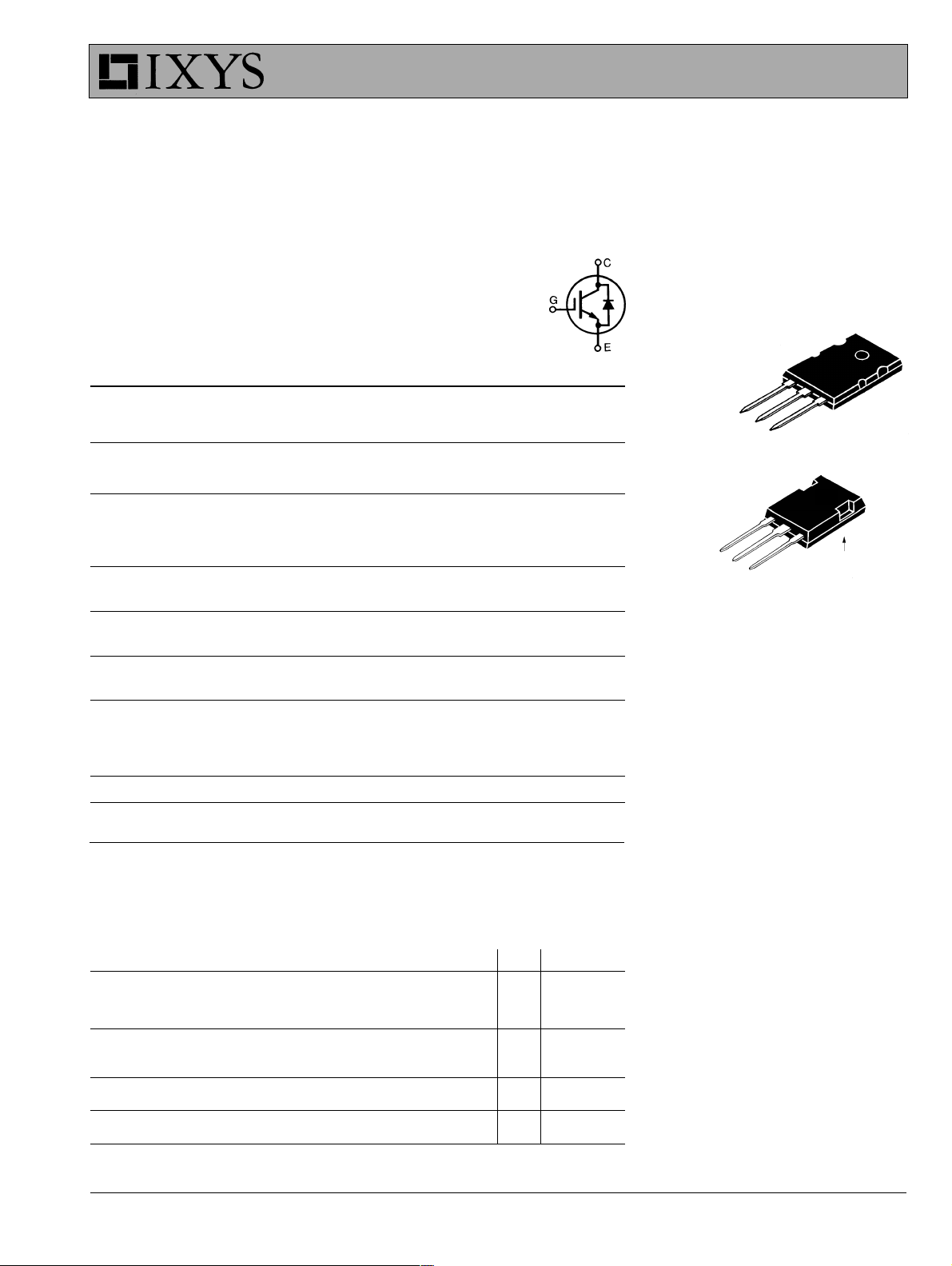
TO-264 AA
(IXSK)
G
C
E
PLUS TO-247
TM
(IXSX)
G
C
E
G = Gate, C = Collector,
E = Emitter, TAB = Collector
C (TAB)
Features
Hole-less TO-247 package for clip
mounting
High frequency IGBT and anti-parallel
FRED in one package
Low V
CE(sat)
- for minimum on-state conduction
losses
MOS Gate turn-on
- drive simplicity
Fast Recovery Epitaxial Diode (FRED)
- soft recovery with low I
RM
Symbol Test Conditions Characteristic Values
(TJ = 25°C, unless otherwise specified)
min. typ. max.
BV
CES
V
GE(th)
I
VCE= 0.8 V
CES
I
GES
V
CE(sat)
Device must be heatsunk for high temperature measurements to avoid thermal runaway.
IXYS reserves the right to change limits, test conditions and dimensions
© 2000 IXYS All rights reserved
IC= 3 mA, VGE = 0 V 1200 V
IC= 250 mA, VCE = V
VGE= 0 V TJ = 125°C3mA
CES
GE
36V
1mA
VCE= 0 V, VGE = ±20 V ±100 nA
IC= I
, VGE = 15 V 3. 6 V
C90
Applications
AC motor speed control
DC servo and robot drives
DC choppers
Uninterruptible power supplies (UPS)
Switch-mode and resonant-mode
power supplies
Advantages
Space savings (two devices in one
package)
Reduces assembly time and cost
High power density
98733 (7/00)

IXSX 35N120BD1
IXSX 35N120BD1
Symbol Test Conditions Characteristic Values
(TJ = 25°C, unless otherwise specified)
min. typ. max.
g
fs
IC= I
; VCE = 10 V, 16 23 S
C90
Pulse test, t £ 300 ms, duty cycle £ 2 %
C
C
C
Q
Q
Q
t
t
t
t
E
t
t
E
t
t
E
R
R
ies
oes
res
g
ge
gc
d(on)
ri
d(off)
fi
off
d(on)
ri
on
d(off)
fi
off
thJC
thCK
VCE = 25 V, VGE = 0 V, f = 1 MHz 315 pF
IC = I
, VGE = 15 V, VCE = 0.5 V
C90
Inductive load, T
IC = I
, VGE = 15 V,
C90
VCE = 0.8 V
Switching times may increase for V
(Clamp) > 0.8 V
increased R
J
, RG = 5.0 W
CES
G
= 2 5°C
, higher TJ or
CES
CES
CE
Inductive load, TJ = 1 25°C
IC = I
, VGE = 15 V,
C90
VCE = 0.8 V
Switching times may increase for V
(Clamp) > 0.8 V
increased R
, RG = 5.0 W
CES
G
, higher TJ or
CES
CE
3600 pF
75 pF
120 nC
33 nC
49 nC
36 ns
27 ns
160 300 ns
180 300 ns
59mJ
38 ns
29 ns
6mJ
240 ns
340 ns
9mJ
0.42 K/W
0.15 K/W
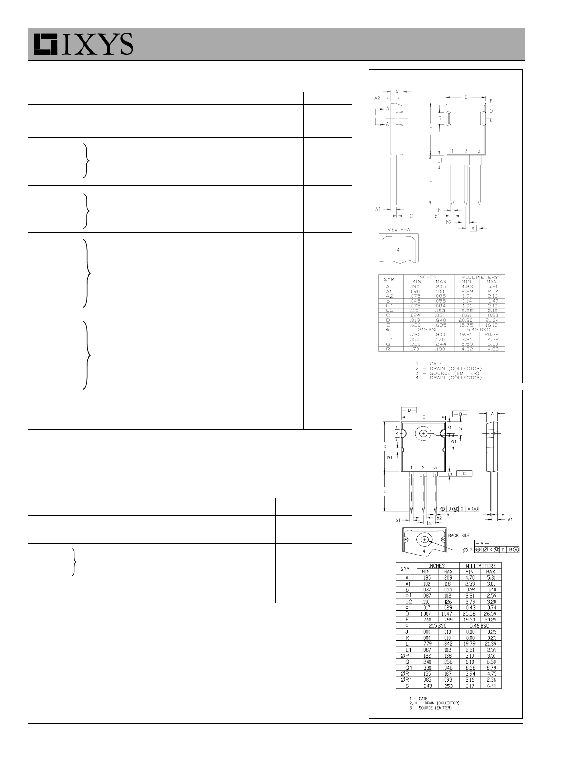
TO-247 HOLE-LESS Outline
TO-264 AA Outline
Reverse Diode (FRED) Characteristic Values
(TJ = 25°C, unless otherwise specified)
Symbol Test Conditions min. typ. max.
V
F
I
RM
t
rr
R
thJC
IXYS reserves the right to change limits, test conditions, and dimensions.
IXYS MOSFETS and IGBTs are covered by one or more of the following U.S. patents: 4,835,592 4,881,106 5,017,508 5,049,961 5,187,117 5,486,715
IF = 130A, VGE = 0 V, Pulse test, 2.75 V
t £ 300 ms, duty cycle d £ 2 %, TJ = 125°C 1.85 V
IF= 130A, VGE = 0 V, -diF/dt = 100 A/msTJ =100°C 7 14.3 A
VR = 100 V
IF= 1 A; -di/dt = 200 A/ms; VR = 30 V 40 n s
0.65 K/W
4,850,072 4,931,844 5,034,796 5,063,307 5,237,481 5,381,025
 Loading...