IXBD4410 / IXBD4411
ISOSMARTTM Half Bridge Driver Chipset
Type Description Package Temperature Range
IXBD4410PI Full-Feature Low-Side Driver 16-Pin P-DIP -40 to +85°C
IXBD4411PI Full-Feature High-Side Driver 16-Pin P-DIP -40 to +85°C
IXBD4410SI Full-Feature Low-Side Driver 16-Pin SO -40 to +85°C
IXBD4411SI Full-Feature High-Side Driver 16-Pin SO -40 to +85°C
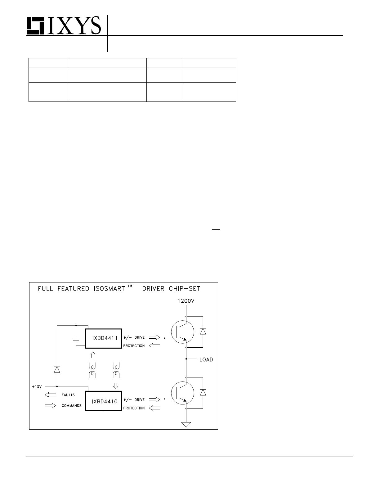
The IXBD4410/IXBD4411
ISOSMART chipset is designed to
control the gates of two Power
MOSFETs or Power IGBTs that are
connected in a half-bridge (phaseleg) configuration for driving
multiple-phase motors, or used in
applications that require half-bridge
power circuits. The IXBD4410/
IXBD4411 is a full-feature chipset
consisting of two 16-Pin DIP or SO
devices interfaced and isolated by
two small-signal ferrite pulse
transformers. The small-signal
transformers provide greater than
1200 V isolation.
Even with commutating noise
ambients greater
than ±50 V/ns and
up to 1200 V potentials, this chipset
establishes error-free two-way
communications between the
system ground-referenced
IXBD4410 and the inverter output-
referenced IXBD4411. They incorporate undervoltage V
and overcurrent or desaturation
or VEE lockout
DD
shutdown to protect the IGBT or
Power MOSFET devices from
damage.
The chipset provides the necessary
gate drive signals to fully control the
grounded-source low-side power
device as well as the floatingsource high-side power device.
Additionally, the IXBD4410/4411
chipset provides a negative-going,
off-state gate drive signal for
improved turn-off of IGBTs or Power
MOSFETs and a system logiccompatible status fault output FLT to
indicate overcurrent or desaturation,
and undervoltage V
a status fault, both devices drive
or VEE. During
DD
their respective gate outputs at VEE,
and keep their driven MOSFETs or
IGBTs off.
Features
● 1200 V or greater low-to-high side
isolation.
● Drives Power Systems Operating on
up to 575 V AC mains
● dv/dt immunity of greater than
±50V/ns
● Proprietary low-to-high side level
translation and communication
● On-chip negative gate-drive supply
to ensure Power MOSFET or IGBT
turn-off and to prevent gate noise
interference
● 5 V logic compatible HCMOS inputs
with hysteresis
● Available in either the 16-Pin DIP or
the 16-Pin wide-body, small-outline
plastic package
● 20 ns switching time with 1000 pF
load; 100 ns switching time with
10,000 pF load
● 100 ns propagation delay time
● 2 A peak output drive capability
● Self shut-down of output in response
to over-current or short-circuit
● Under-voltage and over-voltage V
lockout protection
● Protection from cross conduction of
DD
the half bridge
● Logic compatible fault indication
from both low and high-side driver
540 V-
IXYS reserves the right to change limits, test conditions and dimensions.
I - 1
Applications
● 1- or 3-Phase Motor Controls
● Switch Mode Power Supplies
(SMPS)
● Uninterruptible Power Supplies
(UPS)
● Induction Heating and Welding
Systems
● Switching Amplifiers
● General Power Conversion Circuits
© 2001 IXYS All rights reserved

IXBD4410 / IXBD4411
Symbol Definition Maximum Ratings
VDD/V
EE
V
in
I
in
Io (rev) Peak Reverse Output Current (OUT) 2 A
P
D
Supply Voltage -0.5 to 24 V
Input Voltage (INH, INL) -0.5 to VDD+0.5 V
Input Current (INL, INH, IM) ±10 mA
Maximum Power Dissipation (TA ≤ 25°C)
16 Pin PDIP (PI) 1.6 W
16 Pin SOIC (SI) 1.2 W
θθ
θ
θθ
JA
Thermal Impedance (Junction To Ambient)
16 Pin PDIP (PI) 75 °C/W
16 Pin SOIC (SI) 100 °C/W
T
A
T
JM
T
stg
T
L
Operating Ambient Temperature -40 to +85 °C
Maximum Junction Temperature +150 °C
Storage Temperature Range -55 to +150 °C
Lead Soldering Temperature for 10 s 300 °C
Recommended Operating Conditions
V
DD/VEE
VDD/LG 10 to 16.5 V
LGh/L
Gl
Supply Voltage 10 to 20 V
Maximum Common Mode dv/dt ±50 V/ns
Symbol Definition/Condition Characteristic Values
= 25°C, VDD = 15 V, unless otherwise specified)
(T
A
min. typ. max.
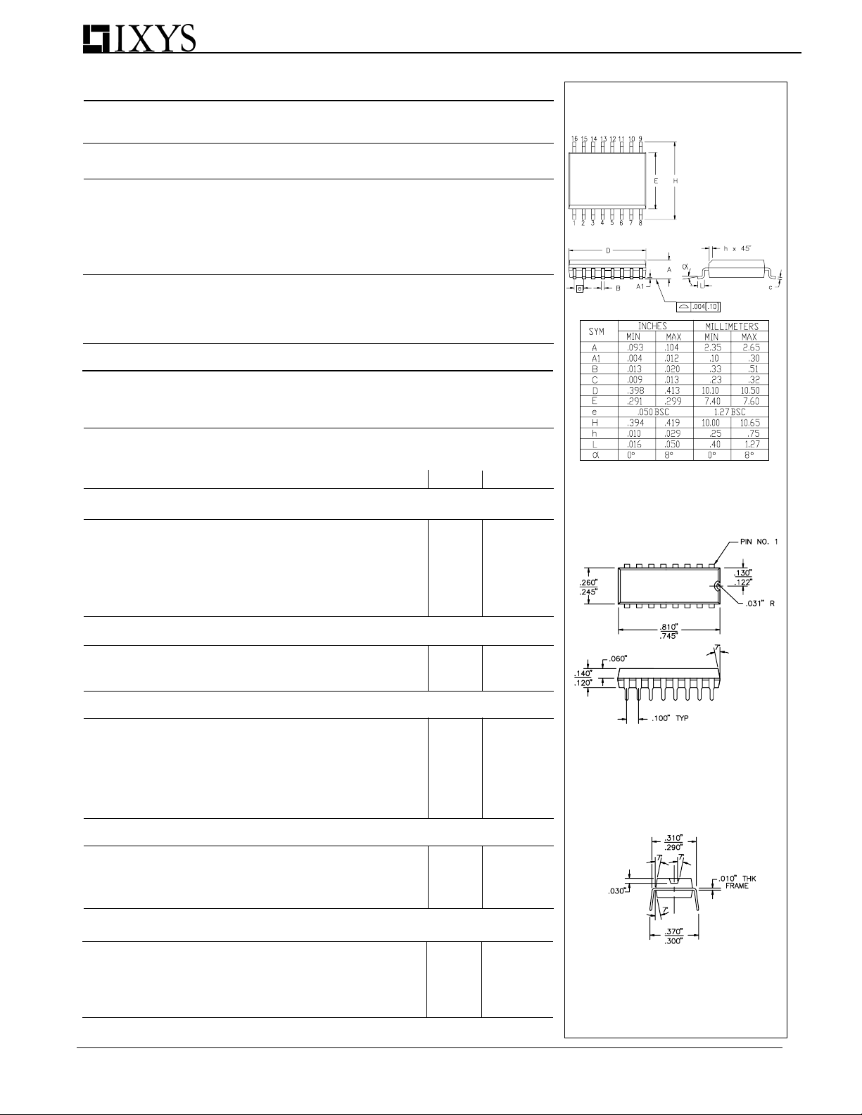
Dimensions in inch (1" = 25.4 mm)
16-Pin SO
INL, INH Inputs (referred to LG)
V
t+
V
t-
V
ih
I
in
C
in
Positive-Going Threshold 3.65 V
Negative-Going Threshold 1.5 V
Input Hysteresis .6 V
Input Leakage Current/Vin=VDD or LG -1 1 µA
Input Capacitance 10 p F
Open Drain Fault Output (referred to LG)
V
oh
V
ol
HI Output/Rpu = 10 kΩ to V
DD
LO Output/Io = 4 mA 0.4 0.7 V
OUT Output (referred to LG)
V
oh
V
ol
R
o
R
o
I
pk
HI Output/Io = -5 mA VDD-0.05 V
LO Output/Io = 5 mA VEE+0.05 V
Output HI Res./Io = -0.1 A 3 5 Ω
Output LO Res./Io = 0.1 A 3 4 Ω
Peak Output Current/CL = 10 nF 1.5 2 A
IM Input (referred to KG)
V
t+
C
in
R
s
Positive-Going Threshold 0.24 0.3 0.36 V
Input Capacitance 10 p F
Shorting Device Output Resistance 80 12 0 150 Ω
16-Pin Plastic DIP
VDD-0.05 V
Cross view
VEE Supply (referred to LG)
V
EE
I
out
f
inv
V
EEF
Output Voltage/Io = 1 mA, Co = 1 µF -5 -5.5 -6.5 V
Output Current/V
Inverting Frequency 35 0 kHz
Undervoltage Fault Indication -4 -4.8 V
I - 2
= 0.70 • V
out
EE
-20 -25 mA
© 2001 IXYS All rights reserved

Symbol Definition/Condition Characteristic Values
(Fig. 1A, T
= 25°C, VDD = 15 V, unless otherwise specified)
A
min. typ. max.
VDD Undervoltage Lockout
V
uv
V
uh
Drop Out 9.5 10.5 11.5 V
Hysteresis 0.1 0.3 0.5 V
Quiescent Power Supply Current
V
I
DD
Current/Vin=VDD or LG, Io = 0 3 8 mA
DD
INL and INH Inputs (Fig. 2a, 2b))
t
d(on)
t
r
t
d(off)
t
f
t
dlh(off)
t
dlh(on)
Turn-on delay time; CL =1nF 250 275 ns
4410
Rise time; CL =10 nF 70 100 ns
4410 or 4411 C
=1 nF 15 20 ns
L
Turn-off delay time CL =1nF 150 175 ns
4410
Fall time CL =10nF 70 150 ns
CL =1nF 15 20 ns
4410 to 4411
Turn-off delay time CL =1nF 250 275 ns
4410 to 4411
Turn-on delay time CL =1nF 270 300 ns
Fault Output Delay for any Fault Conditions (4410/4411)
t
FLT
FLT Delay/R
= 2 kΩ CL = 20 pF 2 3 us
pu
IXBD4410 / IXBD4411
15
OUT
IXBD4410
or
IXBD4411
R2
9
Im
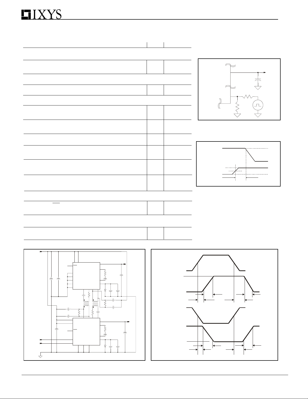
Fig. 1a Overcurrent Detection
VOUT
IXBD4410
or
IXBD4411
5V
VIN
Fig. 1b Overcurrent Delay
R1
to c
4.7K
4.7K
50%
90%
CL
V IN
15V
-5V
+5V
0V
Overcurrent Protection Delay
t
oc
+15V
Driver-Off delay time CL = 10 nF 200 300 ns
(Fig. 1a, 1b)
16
1
Vdd
8
FLT
U2
3
INH
IXBD4411
2
22nF
22nF
INL
(HIGH SIDE)
9
Im
10
KG
11
LG
T+
5
22nF
22
4.7
Ω
7
16
R+
Vdd
1
U1
IXBD4410
8
FLT
(LOW SID E)
3
INH
2
INL
KG Im
LG
11
10 9
+
F
u
uF
7
.
.1
4
.1uF
Ω
T-
46
6
R-
R- R+
22
4
T- T+
OUT
CA
CB
Vee
7
Ω
5
OUT
CA
CB
Vee
1N5817
15
13
12
14
22nF
15
13
12
14
68
.1uF
7
1
8
5
N
1
4.7
68
Ω
.1uF
Fig. 2a: IXBD4410/4411 Switching time test circuit
Ω
F
u
1
.
+
22nF
Ω
22nF
.1uF 4.7uF
+
(IX B D 44 1 0 )
IN L
CL
F
u
7
.
4
+15V
OUT
LOW SID E
-5 V
tr
-5 0%
-9 0%
tf
-1 0%
td (of f)td (on )
(IX BD 4 4 1 0 )
IN H
+15V
CL
OUT
HIGH SIDE
-5 V
(IX B D 44 1 1 )
tf
td lh (o ff)
-5 0%
-
90%
-1 0%
tr
td lh (o n)
Fig. 2b: Output signal waveform
© 2001 IXYS All rights reserved
I - 3

Chipset Overview
This ISOSMARTTM chipset is a pair of
integrated circuits providing isolated
high- and low-side drivers for phase-leg
motor controls, or any other application
which utilizes a half bridge, 2- or 3phase drive configuration. They consist
of two drive control inputs (INL and
INH) for two Power-MOSFET/IGBT
gate-drive outputs. Both inputs operate
from a common ground and are
activated by HCMOS compatible logic
levels. The low-side output operates
near input ground, while the high-side
output operates from a floating ground
that is nominally the source connection
of the high-side phase-leg power
device. Both outputs typically provide
2A of transient current drive for fast
switching of the phase-leg power
device.
IXBD4410 / IXBD4411
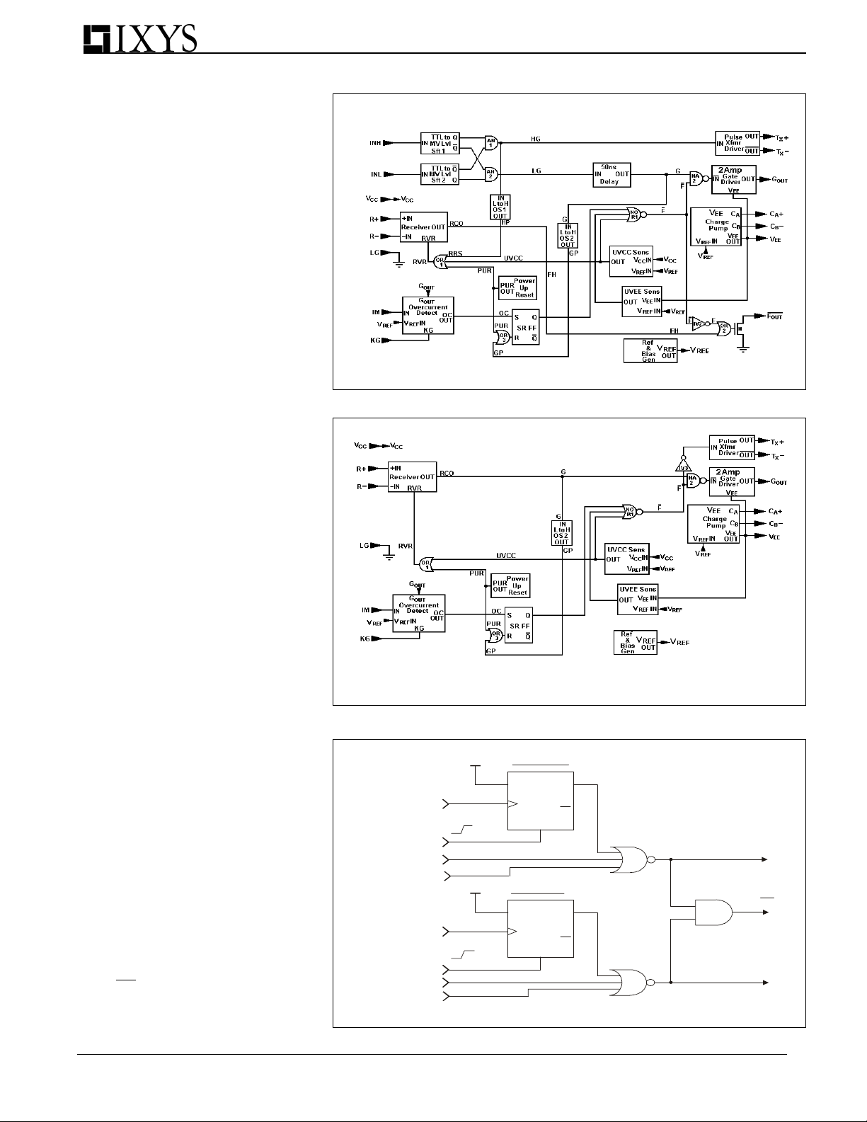
Fig. 3: IXBD4410, low-side driver block diagram
IXBD4410/IXBD4411
The full featured ISOSMART
TM
driver
chipset incorporates an IXBD4410 as
the low-side driver (Fig. 3) and an
IXBD4411 as the high-side driver (Fig.
4). When input "INL" is set to a positive
logic level, the low-side gate output
goes high (turns on); when "INH" is set
to a positive logic level, the high-side
gate drive output goes high. The highside IC is isolated from the low-side IC
by a magnetic barrier, across which the
turn on/off signal is transmitted to the
high-side gate drive. The IXBD4411
fault signal is also transmitted back to
the IXBD4410 driver via these
transformers. This isolation only
depends on the low cost communications transformer, which is designed to
withstand 1200 V or more.
There are two magnetic transmission
channels between the low- and highside IC's for bi-directional communication. One sends a signal from the
low-side IXBD4410 IC up to the highside IXBD4411 IC and the other sends
a signal back from the high-side to the
low-side IC. The signal that is sent up
controls the IXBD4411 gate-drive
output. The signal sent from the
IXBD4411 back to the IXBD4410
indicates a high-side fault has occurred
(overcurrent, or under-voltage of the
high-side + power supplies). This is
detected at the IXBD4410 driver and
sets "FLT" pin low, to indicate the highside fault.
Fig. 4: IXBD4411, high-side driver block diagram
VCC
OVER CURRENT
INH
VDD UNDE R VOLTAGE
VEE UN DE R VO LTAGE
VC C
OVER CURRENT
INL
VDD UNDE R VOLTAGE
VEE UN DE R VO LTAGE
HIGH SIDE
D
R
LO W S ID E
D
R
Q
Q
Q
Q
HIGH-SIDE
OUTPUT ENABLE
FLT
LO W-SIDE
OUTPUT ENABLE
The fault signal that is returned from
I - 4
Fig. 5: Logic Representation of IXBD4410 FLT Signal
© 2001 IXYS All rights reserved
 Loading...