IXYS EVDP610 Datasheet

EVDP610
IXDP610 Digital PWM Controller IC Evaluation Board
General Description
The IXDP610 Digital Pulse Width Modulator (DPWM) is a
programmable CMOS LSI device, which accepts digital
pulse width data from a microprocessor and generates
two complementary non-overlapping pulse width modulated signals for direct digital control of a switching Power
Bridge or other electronics. See the IXDP610 data sheet
for full specifications.
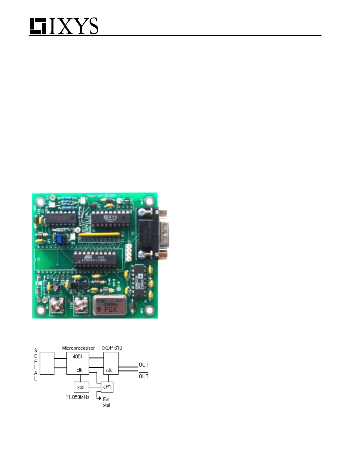
The EVDP610 Evaluation Board, shown in Figure 1 below,
encompasses the serial communications hardware,
microprocessor, and IXDP610 chip all onto one board that
is easily programmable from any PC. A Graphical User
Interface (GUI) designed to run on a Windows 9X, Windows 2000 or Windows NT operating system is included
with the EVDP610, providing the designer with the software and hardware tools to immediately test and evaluate
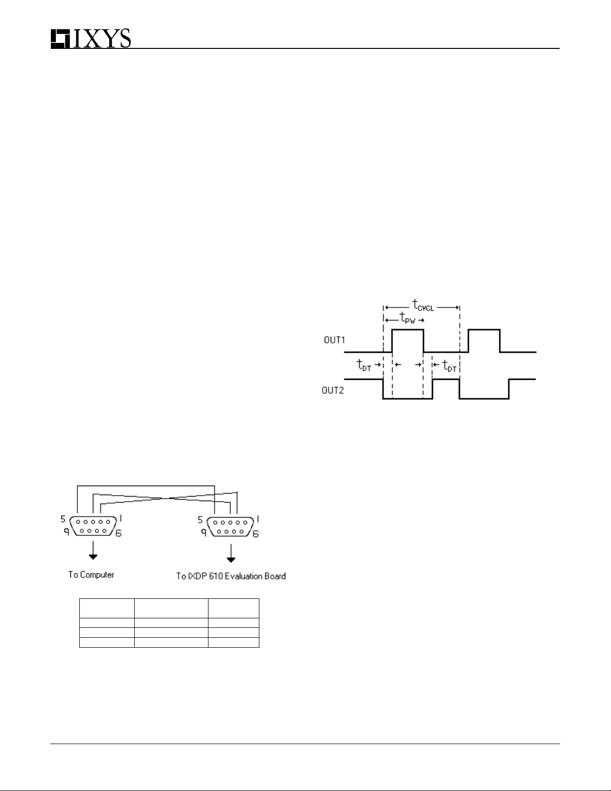
the IXDP610 IC. A functional block diagram of the
EVDP610 is shown in Figure 2.
1.0 EVDP610 QUICK-START INSTRUCTIONS
These quick-start instructions provide a step-by-step
guide to set up and begin using the EVDP610 evaluation
board and software. Please refer to the appropriate
sections of the specification for additional instructions
and guidelines.
1.1 Installing the IXDP610 Evalution Software
To install the Evaluation Software on the comuter, place
the Evaluation Software diskette into the computer's disk
drive. Run setup.exe (or double-click on the setup icon).
Follow the instructions that appear on the screen.
1.2 Powering On the IXDP610 Evaluation Board
1. Connect +5 volts DC (+/- 5%) power to the two
screw terminals labeled TRM1 and TRM 2. TRM 1
is the power terminal and TRM 2 is the ground
terminal. When power is applied the two green
LEDs labeled D1 and D3 will turn on.
2. By default, the evaluation board firmware loads the
pulse width registers of the IXDP610 with a 0% duty
cycle on Output1 and a 100% duty cycle on Output2
(Output1 is labeled TP1 – with a white terminal
attached and Output2 is labeled TP2 – with a black
terminal attached). The LED’s labeled D4 and D5,
corresponding to Output1 and Output2 respectively,
should glow red when the output is disabled. When
the outputs are enabled, the LEDs will glow green.
Figure 1 - EVDP610 Evaluation Board
Figure 2 - EVDP610 Functional Block Diagram
1.3 Connecting the Serial Communications
1. Connect one end of the null modem cable (provided
with the EVDP610) to the male DB9 connector on
the circuit board (labeled P1) and connect the other
end to the serial port. The pin-out of the null modem
cable is shown in the figure 3 below.
1.4 Checking Jumper Connections
1. There should be a jumper in the middle position on
JP1 (allowing the 11.059MHz clock – the same one
clocking the micro, to clock the IXDP610 chip). See
section 2.3 for more information and a detailed
drawing of the jumper positions.
2. There should be NO jumper in JP2 – installing this
jumper disables all outputs on the IXDP610 by
asserting the ODIS pin. The factory default is no
jumper in JP2.
1.5 Operating the User Interface Software
1. The IXDP610 hardware must be powered on before
running the GUI. In the GUI’s initialization sequence
the GUI will try to communicate with the EVDP610
hardware. Be aware that the GUI will reset the
EVDP610 hardware as soon as it comes up and is
Copyright © IXYS CORPORATION 2001
First Release

EVDP610
running after establishing communication. This
assures that both the board and the software are
initialized into the same states to avoid confusion.
2. Make sure that the board is in 8 bit resolution mode
by checking the resolution button (8 bit resolution is
the board's default state). Flip the switch in the
Pulse Settings area so that the pulse width test box
is now no longer dimmed. Enter a number into this
text box between 0 – 255. The duty cycle textbox
will change accordingly although it will remain
dimmed until the switch is toggled, ie: if you enter a
128, the duty cycle will read 50%.
2.0 GENERAL DESCRIPTION AND THEORY OF
OPERATION
For circuit design information, refer to the EVDP610
schematic and PCB layout drawing in Figures 7 and 8.
2.1 Serial Communications
The RS-232 communications interface allow the
EVDP610 to communicate and respond to commands
through a serial port. The serial bus operates at 9600
baud and is buffered by an RS232 driver before reaching
the microprocessor. For more specific information on
the serial protocol please see Section 4.
In this manner the user can easily set pulse width, dead
time, resolution, among other functions such as dividing
the clock signal.
2.2 IXDP610 IC
The IXDP610 chip, labeled U1 on the evaluation board,
generates two complementary non-overlapping, pulse
width modulated signals for direct digital control of a
switching power bridge.
2.2.1 Dead Time
The PWM waveform generated by the IXDP610 results
from comparing the output of the Pulse Width counter to
the number stored in the Pulse Width Latch. A programmable “dead-time” (defined as t
in Fig.4) is incorporated
DT
into the PWM waveform. The Dead-Time Logic disables
both outputs on each transition of the comparator output
for the required dead-time interval. This feature is difficult
to duplicate in equivalent analog system.
To communicate with and control the EVDP610 Board, a
null modem cable (included) must be connected from a
PC’s serial port to the male DB9 connector on the board.
For user reference a pin out of the cable is shown in
Figure 3. Once the correct communications port is
selected, the user can run all of the features of the
IXDP610 chip from the GUI.
Femal e DB9
(computer)
Pin 2 Pin 3 TX
Pin 3 Pin 2 RX
Pin 5 Pin 5 GND
Femal e DB9
(EVDP610 board)
Description
Figure 3 - Null Modem Cable Pin-Out
The GUI software allows the user to set all functions
provided on the IXDP610 with the simple click of a button
or writing into a text box.
Figure 4: Output Waveform Displaying Dead-Time
For example, in a half bridge system the dead time can
prevent two transistors being on at the same time. If both
transistors are on for a short period of time, they could
effectively short the voltage supple to ground, which is an
undesirable situation.
2.2.2 Lock Bit
Setting the lock bit of the IXDP610 prevents all writes to
the control latch except for the Stop bit. This locking
feature prevents modification of the control latch due to
software error, preventing damage to the system being
controlled by the IXDP610. This prevents changing of the
dead-time, clock divide, and resolution settings.
2.2.3 Clock Divide Bit
This feature allows the IXDP610 to divide the input clock
by one or divided by two.
2.2.4 Resolution
The IXDP610 can run in two resolution modes, 8-bit and
7-bit. Choosing 7-bit resolution doubles the achievable
PWM base frequency at the expense of decreased duty
cycle resolution. With the combination of the Divide bit
(labeled Clock Divide on the GUI) and the resolution bit,
2
 Loading...