

IXYS DSS17-06CR Datasheet
DSS 17-06CR
HiPerDynTM Schottky Diode
(Electrically Isolated Back Surface)
Preliminary Data
V
RSM
V V
600 600 DSS 17-06CR
Symbol Conditions Maximum Ratings
I
FRMS
I
FAVM
I
FRM
I
FSM
E
AS
I
AR
T
VJ
T
VJM
T
stg
P
tot
V
ISOL
F
C
Weight typical 6 g
V
RRM
Type
A
50 A
TC = 95°C; rectangular, d = 0.5 17 A
tP < 10 µs; rep. rating, pulse width limited by T
VJM
tbd A
TVJ = 45°C; tp = 10 ms (50 Hz), sine 200 A
TVJ = 25°C; non-repetitive tbd mJ
IAS = 2 A; L = 180 µH
VA = 1.5·VR typ.; f = 10 kHz; repetitive tbd A
-55...+175 °C
175 °C
-55...+150 °C
TC = 25°C 105 W
50/60 Hz RMS; I
≤ 1 mA 2500 V~
ISOL
mounting force with clip 20...120 N
I
FAV
V
t
rr
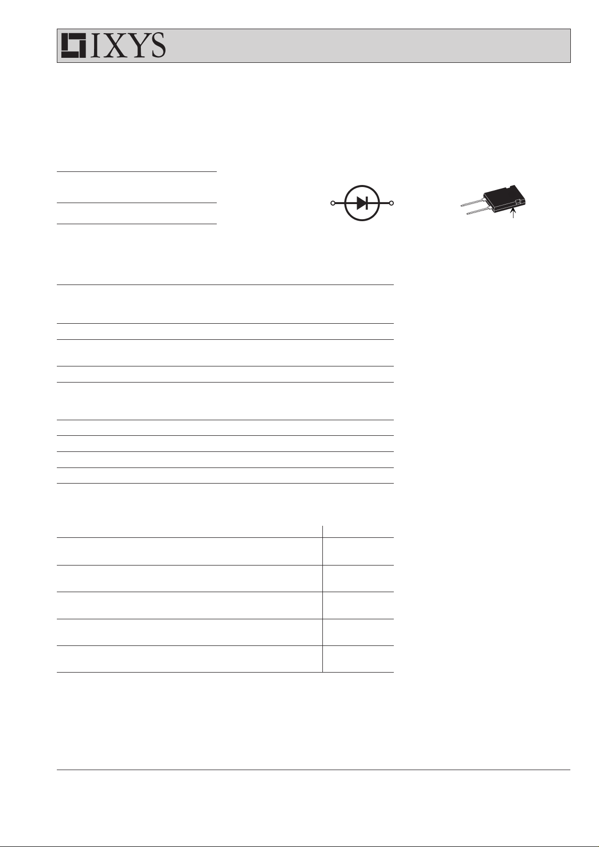
ISOPLUS 247
C
A = Anode, C = Cathode
* Patent pending
RRM
= 17 A
= 600 V
= 45 ns
TM
C
A
Isolated back surface *
Features
●
Silicon chip on Direct-Copper-Bond
substrate
- High power dissipation
- Isolated mounting surface
- 2500V electrical isolation
●
Low cathode to tab capacitance (<25pF)
●
International standard package
●
Planar passivated chips
●
Very short recovery time
●
Extremely low switching losses
●
Low IRM-values
●
Soft recovery behaviour
●
Epoxy meets UL 94V-0
●
Isolated and UL registered E153432
Symbol Conditions Characteristic Values
typ. max.
IR① TVJ = 25°C VR= V
TVJ = 125°C VR= V
VF② I
= 15 A; TVJ= 125°C 2.71 V
F
RRM
RRM
0.5 mA
5mA
TVJ= 25°C 3.32 V
R
thJC
R
thCH
t
rr
IF = 10 A; -di/dt = 100 A/µs; 45 ns
0.25 K/W
1.4 K/W
VR = 100 V; TVJ = 25°C
I
RM
VR = 100 V; IF = 10 A; -diF/dt = 100 A/µs 4.0 A
TVJ = 25°C
Pulse test: ① Pulse Width = 5 ms, Duty Cycle < 2.0 %
② Pulse Width = 300 µs, Duty Cycle < 2.0 %
Data according to IEC 60747 and per diode unless otherwise specified
IXYS reserves the right to change limits, test conditions and dimensions.
© 2000 IXYS All rights reserved
Applications
●
Antiparallel diode for high frequency
switching devices
●
Antisaturation diode
●
Snubber diode
●
Free wheeling diode in converters
and motor control circuits
●
Rectifiers in switch mode power
supplies (SMPS)
●
Inductive heating
●
Uninterruptible power supplies (UPS)
●
Ultrasonic cleaners and welders
Advantages
●
Avalanche voltage rated for reliable
operation
●
Soft reverse recovery for low EMI/RFI
●
Low IRM reduces:
- Power dissipation within the diode
- Turn-on loss in the commutating
switch
Dimensions see outlines.pdf
048
1 - 2

DSS 17-06CR
100
A
I
F
10
T
VJ
175°C
150°C
125°C
25°C
1
012345
V
F
Fig. 1 Maximum forward voltage
drop characteristics
30
A
25
I
F(AV)
20
15
10
d=0.5
DC
10
mA
TVJ=175°C
1000
pF
1
150°C
I
R
125°C
C
T
0.1
0.01
100°C
75°C
50°C
=
100
0.001
25°C
0.0001
V
0 200 400 600
Fig. 2 Typ. value of reverse current I
versus reverse voltage V
V
V
R
R
R
10
0 200 400 600
Fig. 3 Typ. junction capacitance C
versus reverse voltage V
TVJ= 25°C
V
V
R
T
R
70
W
60
P
(AV)
50
I
A
FSM
d =
40
DC
0.5
30
0.33
0.25
0.17
20
0.08
5
0
04080120160
T
C
Fig. 4 Average forward current I
versus case temperature T
°C
F(AV)
C
10
0
5152501020
I
F(AV)
Fig. 5 Forward power loss
characteristics
A
t
2
1
D=0.5
K/W
0.33
Z
thJC
0.25
0.17
0.08
0.1
Single Pulse
t
DSS17-06CR
s
0.01
0.0001 0.001 0.01 0.1 1 10
Fig. 6 Transient thermal impedance junction to case at various duty cycles Note: All curves are per diode
µs
P
© 2000 IXYS All rights reserved
2 - 2
 Loading...