Page 1

I
NTEGRATED CIRCUITS DIVISION
CPC5902G/CPC5903G
Evaluation Board
User’s Guide
JP9
R2
VDDA
GNDA
VDDA
1001
1001
JP1
GNDA
R1
C1
CPC5902/3
JP2
SCLA
SDAA
JP4
JP3
R3
1001
1001
R4
C3
04-26-12
CPC5902/3-EVAL. PCB
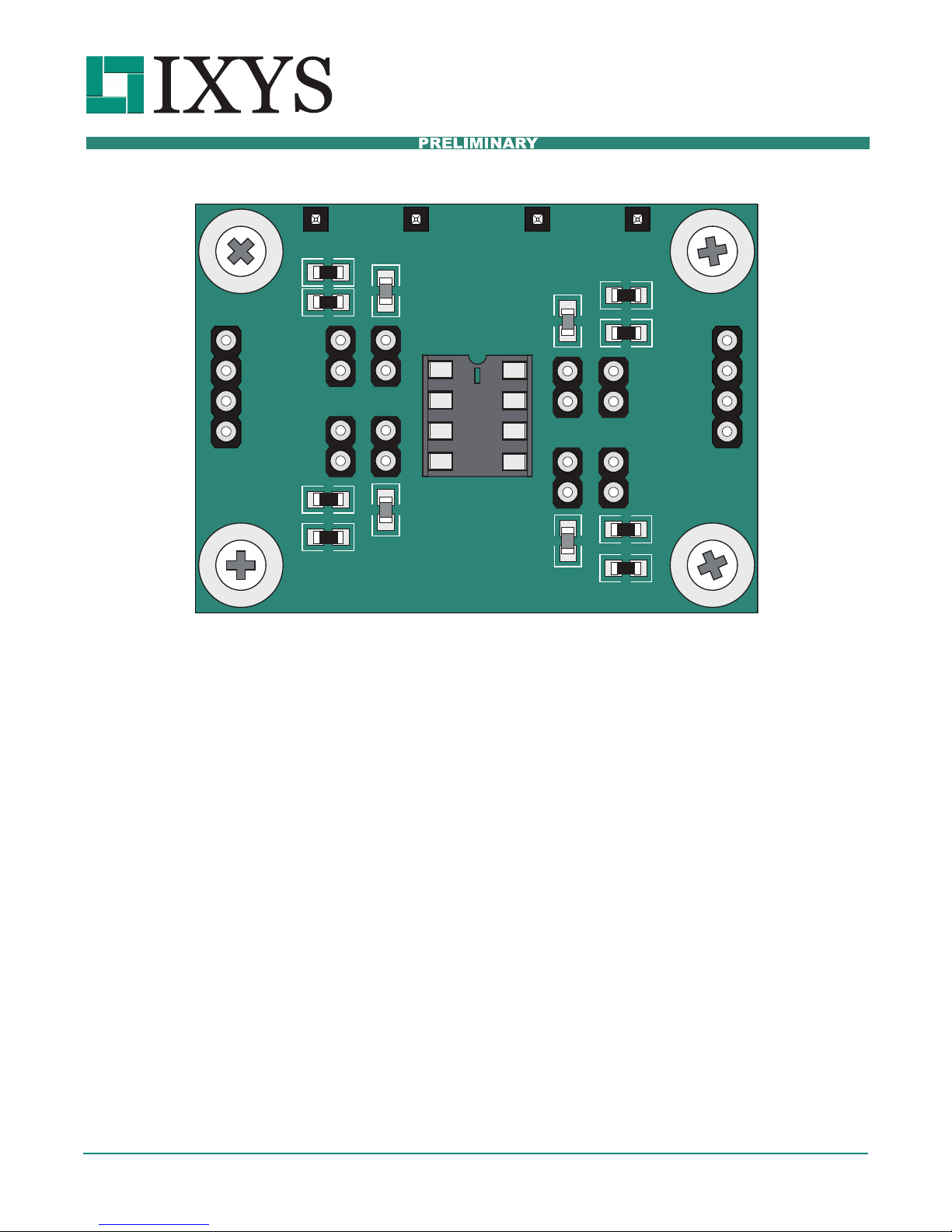
The CPC5902G/5903G Evaluation Board can be used
2
to isolate an I
obtainable when communicating between the user's
2
I
C devices. The 8-pin DIP socket can be populated
with either a CPC5902G (for both SCL and SDA
bidirectional) or with a CPC5903G (for SDA
bidirectional, SCL sideA to sideB only).
At the left side of the board are four 0.1 inch centered
posts that carry VDDA, GNDA, SCLA and SDAA. See
the drawing above for signal, component, and jumper
locations. Best performance will result if the VDDA and
GNDA posts are connected to the same VDD and
GND as the sideA I
should be connected to the I
the bus master on sideA. In addition, the SDAA post
should be connected to the I
bus master. On the right side of the board there are
four posts which carry VDDB, GNDB, SCLB and
SDAB when connected to the sideB I
C bus, and to evaluate the performance
2
C bus master. The SCLA post
2
C serial clock line SCL at
2
C serial data line at the
2
C devices.
GNDB
VDDB
R6
C4
2701
R5
1501
JP10
VDDB
GNDB
SCLB
JP6
SDAB
1501
2701
JP8
R7
JP7
C6 JP5
R8
At the top left of the board are duplicate posts, which
are electrically shorted to the VDDA and GNDA posts
on the left side of the board. These two posts enable
convenient operation in standalone mode, when a full
2
I
C bus may not be available at sideA. Similarly, at the
top right of the board, there are duplicates of the
VDDB and GNDB posts. The CPC5902G and
CPC5903G will each operate correctly for
2.7V < VDDA < 5.5V and 2.7V < VDDB < 5.5V.
While it is possible to attach a second lab power
supply to VDDA, which is not identical to the supply at
the bus master on sideA, and to operate the board
with a live I
mode of operation. The same is true for connecting a
second, non-identical lab power supply to VDDB. The
V
and VIH voltages at the bus isolator are derived
IL
from the VDDA and VDDB voltages. Thus, the
switching thresholds will differ, and noise rejection of
the bus will be worse if the voltage at VDDA is not
identical to the voltage at the VDD connected to the
devices as well as any pull-up resistors on the rest of
the sideA bus segment. Similarly, VDDB should be the
same voltage used at the devices and any pull-ups on
the sideB bus. If either of VDDA or VDDB is not the
2
C interface, this is not the recommended
UG-CPC590x_EvalBd-R00A PRELIMINARY 1
Page 2

I
NTEGRATED CIRCUITS DIVISION
CPC5902G/CPC5903G Evaluation Board
User’s Guide
same as that used at devices on their buses, the
performance of the actual system at power up will not
be observable. VDDA does not need to be the same
value as VDDB, but, as mentioned above, should be
the same voltage as used on the rest of the sideA bus
segment.
The posts at JP1 on the SCLA line can be used with a
0.1-inch header jumper to add 500 (nominal) of
pull-up resistance to the SCLA line. Similarly JP3 adds
500 of pull-up resistance to the SDAA line. These
jumpers are generally not used if there are already
minimum value pull-up resistors elsewhere on the bus.
For operation at 3.3V at VDDA and a bus driver
delivering 0.4V active low, the I
current will be
OL
2.9V/500 = 5.8mA. This is close to the minimum
guaranteed value of 6mA for I
2
C fast mode. For
operation at 5V, this resistance should be increased:
5.0-0.4=4.6V and 4.6V/6mA = 766. The 500 has
been implemented by using R1=R2=1k in parallel. A
quick way to evaluate a 5V system would be to use a
soldering iron to remove either R1 or R2 to increase
the resistance to 1k; however, slightly faster
operation would result from using a pull-up resistor of
perhaps 820.
0.4V and sink 3.01mA. The CPC5902G/5903G drivers
at sideB are only rated for 3mA when used at VDDB
less than 4.5V. The sideB drivers are rated for 6mA
operation at up to 5.5V. At 5.5V, they will drive to
0.23*5.5=1.265V and will pull 4.4mA if the pull-up is
unchanged. At 5.5V, the pull-up resistor would need to
be larger than 705 to limit I
to less than 6mA.
OL
In systems with significant cable length, it is often
preferred to split the pull-up resistance by paralleling a
physical resistor at both ends of the non-isolated bus
segment. To evaluate the performance of a bisected
pull-up, a soldering iron can be used to remove either
R1 or R2, and a 1k resistor (for a 3.3V system) can
be added, if necessary, near the bus master on the
sideA bus segment.
The 2 posts at JP2 and JP4 can be jumpered to add
390pF of capacitive load to the SCLA and SDAA lines.
These jumpers can be used to load the I
2
C lines to I2C
fast mode’s worst case: 400pF in standalone mode.
The jumpers can also be used to add capacitance to
the sideA bus segment if it is extremely lightly loaded,
but loading beyond 400pF total does not guarantee
operation at 400kHz by the I
2
C fast mode
specification.
On the right side, the posts at JP5 and JP7 can be
used to add 964 pull-ups to the SCLB and SDAB
lines. For VDDB = 3.3V and V
= 0.23VDDB=0.76V,
OL
this would yield 3.3 - 0.76 = 2.54V across 964, or
2.635mA of output current sunk by the sideB drivers.
Other devices on the sideB bus might drive to V
OL
=
2 PRELIMINARY R00A
Page 3

I
NTEGRATED CIRCUITS DIVISION
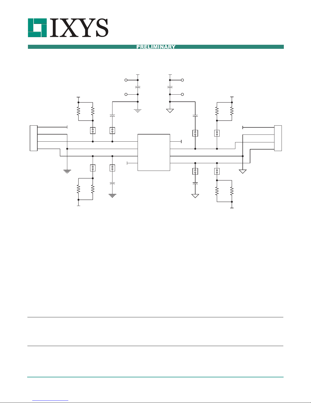
1. Evaluation Board Schematic
*Note: C2 and C5 are located on the bottom side of the board
For additional information please visit www.ixysic.com
IXYS Integrated Circuits Division makes no representations or warranties with respect to the accuracy or completeness of the contents of this publication and reserves the right to make
changes to specifications and product descriptions at any time without notice. Neither circuit patent licenses nor indemnity are expressed or implied. Except as set forth in IXYS Integrated
Circuits Division’s Standard Terms and Conditions of Sale, IXYS Integrated Circuits Division assumes no liability whatsoever, and disclaims any express or implied warranty, relating to its
products including, but not limited to, the implied warranty of merchantability, fitness for a particular purpose, or infringement of any intellectual property right.
The products described in this document are not designed, intended, authorized or warranted for use as components in systems intended for surgical implant into the body, or in other
applications intended to support or sustain life, or where malfunction of IXYS Integrated Circuits Division’s product may result in direct physical harm, injury, or death to a person or severe
property or environmental damage. IXYS Integrated Circuits Division reserves the right to discontinue or make changes to its products at any time without notice.
Specification: UG-CPC590x_EvalBd-R00A
Copyright © 2015, IXYS Integrated Circuits Division
All rights reserved. Printed in USA.
1/26/2015
CPC5902G/CPC5903G Evaluation Board
User’s Guide
JP9
V
DDA
V
DDA
V
DDA
R11kR2
1k
VDDA
1
GNDA
2
SCLA
3
SDAA
4
GNDA
V
DDA
JP1 JP2
JP3 JP4
R3
R4
1k
1k
V
DDA
GNDA
C1
390pF, 50V
V
DDA
C3
390pF, 50V
C2
0.1µF, 50V
GNDA
DUT
1
IOA1
2
GNDA
3
IOA2
4
V
CPC5902/3
*
DDA
GNDB
V
DDB
IOB1
GNDB
IOB2
V
DDB
V
C5
*
0.1µF, 50V
GNDBGNDA
180pF, 50V
8
V
DDB
7
6
5
180pF, 50V
DDB
C4
C6
GNDB
JP5
JP7
V
DDB
R5
1.5kR62.7k
V
DDB
JP6
JP8
R7
1.5kR82.7k
V
DDB
GNDB
VDDB
GNDB
SCLB
SDAB
JP10
1
2
3
4
R00A PRELIMINARY 3
 Loading...