

Page 1
I
NTEGRATED CIRCUITS DIVISION
1. Introduction
CPC5622-EVAL-600R
LITELINK™ III Evaluation Board
User’s Guide
Thank you for using IXYS IC Division’s
CPC5622-EVAL-600R ev aluation board. The
evaluation board ships with the CPC5622A
LITELINK III and CPC5712U Voltage Monitor to
demonstrate the functionality of a PSTN terminating
two-wire interface that provides both the analog v oice
transmission and signaling functions. The analog
interface is configured to provide a 600 resistive AC
impedance with 0dB gain in both the transmit and
receive directions. While the CPC5622A provides the
hook-switch and ringing detect signaling functions, the
CPC5712U is utilized to monitor and detect changes
in the DC line voltage to determine loop status and
signaling information sent by the network. Loop status
is given by the logic level outputs of t he thr ee
CPC5712U on-board detectors indicating Loop
Presence, Line In Use, and Loop Polarity.
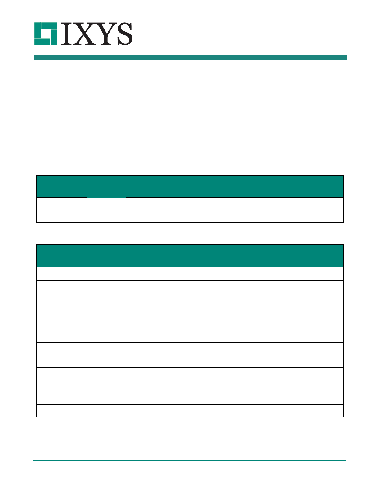
CPC5622-EVAL-600R ev aluation board top a nd
bottom views are shown in the following illustrations.
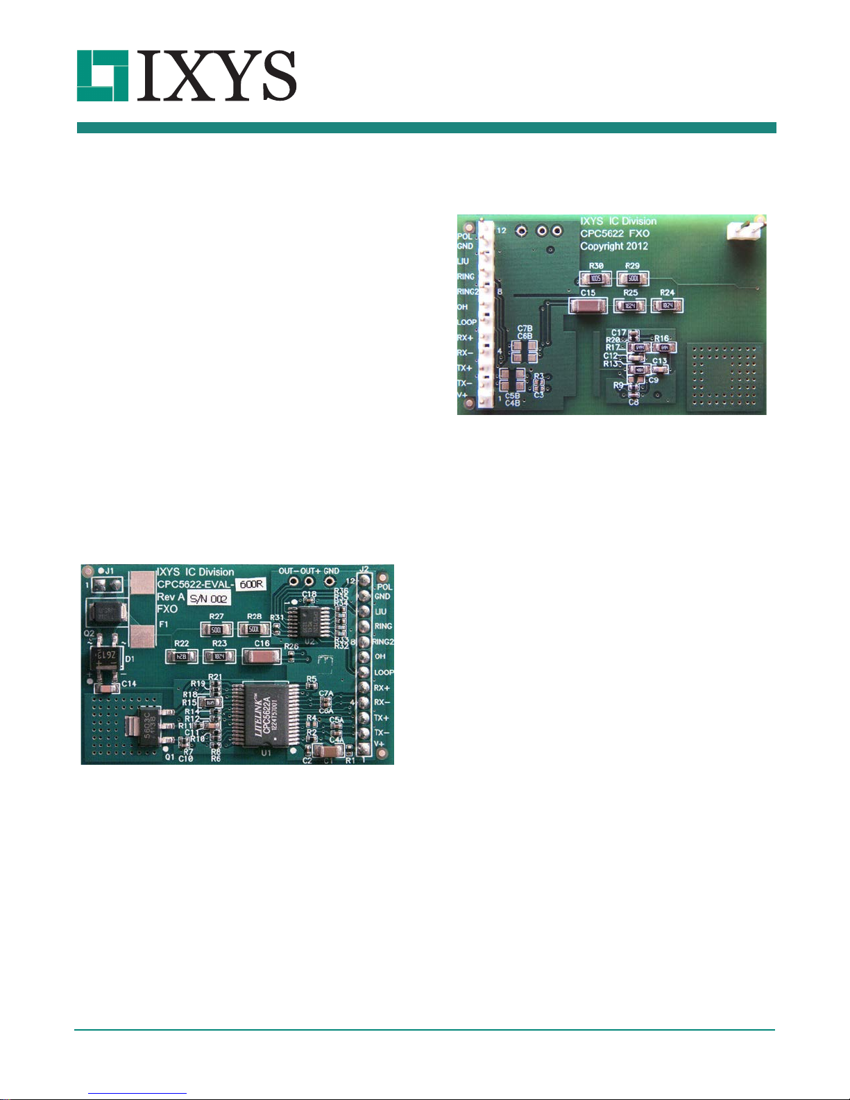
Figure 1. Evaluation Board Top View
Figure 2. Evaluation Board Bottom View
The printed-circuit board used for the
CPC5622-EVAL-600R eva luation board is a
multi-purpose board that facilitates prototyping of
many PSTN line interface configur ations by simple
component changes. Specific evaluation board
models provided by IXYS IC Division can be identified
by the label appended to the core part number
“CPC5622-EVAL-”. The suffix label “600R” as shown
in Figure 1 for this model indicates the two-wire AC
input impedance is 600. For the 600R model, the
transmit and receive gains are 0dB.
• 600R = 600 resistive AC termination with 0dB
transmit and receive gains.
In addition to the model identification label some
boards may hav e a second label located just belo w
the evaluation board part number indicating the
evaluatio n board’s serial number.
UG-CPC5622-EVAL-600R - Rev A www.ixysic.com 1
Page 2
I
NTEGRATED CIRCUITS DIVISION
LITELINK III Evaluation Board Users Guide
2. Setup and Using the Evaluation Board
This section describes setting up the CPC5622-EVAL-600R Evaluation Board prior to use.
2.1 Connections
The CPC5622-EV AL-600R evaluation board uses two
100 mil (2.54 mm) pitch pin headers, J1 and J2, for the
input and output connections. IXYS IC recommends
constructing header jumpers to bring the connections
out to your development or test platform. Connector
PSTN loop connections while J2, the 12-position pin
header, pro v ides access for the low voltage side
power, logic control, logic-level loop status detector
outputs and the analog transmit and receiv e voice
paths.
J1, the two-position pin header, provides access to the
Table 1: Telephone Network Access Connector - J1
Pin
Silk
Screen
Schematic
Name
Use
1 1 RING Connect to the Ring (B) lead of the telephone network or a loop simulator.
2 TIP Connect to the Tip (A) lead of the telephone network or a loop simulator.
Table 2: Low Voltage Side Power and Signal Connector - J2
Pin
Silk
Screen
1V+ VCC
Schematic
Name
Use
Power input: +3.3 V
or +5 V
DC
DC
2 TX- TX-_IN Inverting analog input to the LITELINK
3 TX+ TX+_IN Non-inver ting analog input to the LITELINK
4 RX- RX-_OUT Negative analog output from LITELINK
5 RX+ RX+_OUT Positive analog output from LITELINK
6 LOOP LOOP Loop Presence detector output
7 OH OH* Hook switch control. Off-Hook: OH* = 0, On-Hook: OH* = 1
8 RING2 RING2* Full-wave ringing detector output
9 RING RING* Half-wave ringing detector output
10 LIU LIU* Line In Use detector output
11 GND Low voltage side ground
12 POL POLARITY Polarity Detector output
NOTE: For clarity and con sistency with the schematic, the schematic names will be used from this point forward
throughout the text.
2 www.ixysic.com UG-CPC5622-EVAL-600R - Rev A
Page 3

I
NTEGRATED CIRCUITS DIVISION
LITELINK III Evaluation Board Users Guide
2.2 Using the Evaluation Board
Follow these guidelines for productive use of the LITELINK evaluation board:
• Evaluation board circuit components are sensitiv e to
electrostatic discharge (ESD). Use normal ESD
precautions when working with the LITELINK III
evaluation board.
• Make all low volt age side connections ( J2) to the
board before applying pow er to VCC.
Tip and Ring connections at J1 can be made at any
time before or after VCC power is applied.
• OH* should be open or tied to the VCC input power
pin during power up and held for 50us after power
up.
• Pulling OH* low will cause the CPC5622 to go
off-hook and returning OH* high will cause the unit to
go back on-hook.
3. Functional Description
• Analog transmission in both the transmit path and
the receive path is enabled while of f-hook. When
on-hook, only the receive path is enabled.
• For proper off-hook operation, t he Tip and Rin g
interface must be appropriately biased and
terminated.
• The CPC5622 RING* and RING2* ringing detectors
are only active while on-hook.
• The CPC5712U line voltage and polarity detectors
are active in both the on-hook and off-hook states .
The CPC5622-EVAL-600R provides the analog
interface and signaling functions necessary to
implement a PSTN two-wire terminating device f or
voice and data applications such as PBX FXO,
cordless telephones, FAX machines, set top boxes,
card readers, ATMs, and modems. Analog gains in
both the transmit and receive paths for the 600R
evaluation board are se t to 0dB with the impedance of
the two-wire interface conf igured for 600 ohms
resistive. These analog functions are provided by the
CPC5622A Phone Line Interface integrated circuit.
Additionally, the CPC5622A provides the basic
signaling functions of loop closure / loop open and
ringing detect that are required for a tw o-wire, current
sink, loop start interface. It is important to note that it is
not within the scope of this document to provide
complete behavioral descriptions of the CPC5622A or
the CPC5712U functions as this information is
covered in the data sheets and t he appropriate
application notes.
Basic signaling functions for a loop start, current sink
interface are loop closure (Off-Hook), loop open
(On-Hook) and ringing detect. Loop closure / open is
provided by the hook switch control function with
ringing detect provided by the Snoop input circuit and
the internal ringing detector. Additional loop voltage
detectors used to determine the line status are
provided by the CPC5712U Voltage Monitor with
Detectors integrated circuit. Line condition status
provided by the CPC5712U v oltage detectors are:
Line In Use (LIU), Loop battery presence (LOOP), and
Polarity. While these detectors are not required for the
most basic applications, they are required by the
majority and are therefor provided on the evaluation
board. Access to the analog paths and the detector
functions is provided by the two connectors J1 and J2.
Tip and Ring loop access is provided by J1 while J2
provides access to the low voltage side (SELV) po wer
and signals.
UG-CPC5622-EVAL-600R - Rev A www.ixysic.com 3
Page 4

I
NTEGRATED CIRCUITS DIVISION
LITELINK III Evaluation Board Users Guide
This evaluation board diff ers from pre viou s generation
evaluation boards by incorporating a common mode
noise cancellation circuit that improves longitudinal
balance and common mode rejection across the voice
band spectrum. This is accomplished by using a small
capacitance from shapes on the printed circuit board
(PCB) and modifications to the recommended passive
components values that set the analog transmission
parameters. Details in the construction of the PCB
capacitor are provided in the ev aluation board’s
printed circuit board design files available on line.
3.1 Connector J1 - Tip and Ring
Connector J1, the two-pin header, provides access to
the Tip and Ring (T/R) terminals of the evaluation
board. The Ring lead is located on pin 1 of the
connector and pin 2 is the Tip lead. Although the
board’s layout is designed for lightning and power
cross surge testing, the connector and it’s 25 mil
square pins are not rated for the peak voltages or
currents specified in the safety regulations. It is
suggested the connector be removed and lead wires
be soldered to the board when performing these tests.
3.2 Connector J2 - Low Voltage Side Interface
ended, short one of the input pins to ground and apply
the analog signal to the other input. Typically, TX- is
shorted to ground and the signal is applied to TX+. For
single ended applications, the maximum input signal is
still 0dBm. (This is 1.095Vp.)
Pin 4: RX-_OUT
Pin 5: RX+_OUT
Pins 4 and 5 are the analog voice negative (RX-) and
positive (RX+) differential outputs for the receive path
(T/R to SELV). The maximum output signal by these
pins is 0dBm. This is 0.548Vp on each output.
For single ended receiv e applications, connect one of
the output pins to the receiver input pin and le ave the
other output open. This will result in a receive pat h
loss of 6dB.
Pin 6: LOOP
This is a logic level output indicating the presence of
loop battery feed from the network. For tip to ring
voltages greater than approximately +/-5V
DC
the
detector will output a logic high (LOOP = 1) and for
T/R voltages less than approximately +/-3V
DC
the
detector will output a logic low (LOOP = 0). The LOOP
detector is polarity insensitive.
Providing access to the low v oltage side analog and
digital interface is connector J2, a single row 12-pin
header connector with 25 mil square pins on 100 mil
centers. Due to space limitations, the silkscreen pin
names where modified slightly from the net names
shown on the schematic. These naming differences
are shown in Table 1 and Table 2 on Page 2.
Pin 1: VCC
Po w er pin for the low voltage (SELV) side circuits.
Apply a nominal 3.3V
or 5VDC with respect to the
DC
ground (GND) connection at Pin 11.
Pin 2: TX-_IN
Pin 3: TX+_IN
Pins 2 and 3 are the analog voice negativ e ( TX-) and
positive (TX+) diff er ential in puts for the transmit path
(SELV to T/R). The maximum signal applied to these
input pins is 0dBm. (This is 0.548Vp on each input.)
For applications where the analog source is single
Pin 7: OH*
OH* is an active low, TTL compatible, logic level in put
used to control the hook switch function of the T/R
network interface. Applying a logic low (OH* = 0) at
this pin will enable the gyrator located on the line side
causing DC current to flow. This is commonly referred
to as the “Off-Hook” state. The gyrator, an electronic
inductor, has a low impedance at DC but a high
impedance in the voice band allowing the two-wire
interface to draw DC loop current without loading the
AC termination. An On-Hook state occurs when
OH* = 1 and loop current ceases.
The OH* net is connected to the OH
input at pin 8 of
the CPC5622A. The CPC5622A requires this input to
be left open or pulled high to VCC during power up
and for a minimum dur ation of 50us following power
up. An internal pull-up resistor at the OH
input
provides the required logic high when the input is left
open.
4 www.ixysic.com UG-CPC5622-EVAL-600R - Rev A
Page 5

I
NTEGRATED CIRCUITS DIVISION
LITELINK III Evaluation Board Users Guide
Pin 8: RING2*
This is the full wave ringing detect output RING2
CPC5622A. The output signal will be a logic low
whenever the incoming ringing signal e xceeds the
threshold of the CPC5622A internal voltage detector.
With ringing applied, the output will be a series of
negative pulses at twice the frequency of the ringing
signal. The width of the negative pulses will be a
function of the ringing signal amplitude.
Pin 9: RING*
This is the half-wave ringing detect output RING
CPC5622A. The description of this output signal is
similar to RING2
the same frequency as the incoming ringing signal.
Pin 10: LIU*
LIU* is a logic lev el output indicating an off- hook by
another device on tip and ring whenever the
CPC5622A is on-hook. With a T/R voltage less than
approximately +/-14V
(LIU* = 0) is output. For tip to ring voltages greater
than approximately +/-17V
logic high (LIU* = 1). As with the LOOP detector, the
LIU* detector is polarity insensitive.
above but the output pulses will hav e
an Off-Hook indication
DC
the detector will output a
DC
of the
of the
3.3 Tip to Ring Conditioning
When using the CPC5622 ev alu ation board, t he tip t o
ring interface must be properly configured with DC
bias for off-hook A C transmission as the CPC5622 line
side circuitry derives it’s operating po w er from t he
network. In addition, the CPC5622 must have a tip to
ring AC termination impedance equal to the evaluation
board’s two-wire input impedance for correct analog
transmission performance. The required tip to ring
termination impedance for the CPC5622-EVAL-600R
evaluatio n board is 600.
For basic functional testing, the tip and ring may be
connected to an external PSTN line. While these lines
provide DC bias and an acceptable A C t ermination for
access to the network, they are not suitable for lab
quality measurements.
General purpose evaluations can be made using a
phone line simulator , a lso known as a Central Office
(CO) line simulator, to source the DC loop current and
to provide a reasonable AC impedance. Using a line
simulator rather than an external PSTN line eliminates
the variable AC impedance and DC feed
characteristics caused by the outside cable plant.
Declaring the line to be Off-Hook when LIU* = 0 is
only valid when loop battery is present, LOOP = 1.
Pin 11: GND
This is the low voltage side ( SELV) ground. All low
voltage side signals are referenced from this net. The
tip and ring voltages as well as the line side signals
are NOT ref erenced from the lo w v oltage side ground.
Pin 12: POLARITY
POLARITY is a logic level out put that indicates the
polarity of the battery feed on tip and ring.
POLARITY = 1 for normal battery when the Tip is
more positive than the Ring. When the battery polarity
is reversed causing Ring to be mor e positiv e than Tip,
the detector will output POLARITY = 0. The
POLARITY detector nominal thresholds are set at
.
2V
DC
The POLARITY detector does not change state until
the increasing line voltage potential passes through
the switching point. This ensures the POLARITY
detector output will remain stable at it’s last state if
battery feed from the network is lost.
Lab quality measurements are typically made using a
DC feed circuit conforming to industry standards and
test equipment specific for voice quality testing.
3.4 Analog Transmission
The UG-CPC5622-EVAL-600R evaluation board
supports full duplex analog voice transmission while
off-hook and receive transmission only when on-hook.
The nominal gains for all of these tr ansmission paths
is 0dB.
3.5 Loop Status Detectors
In addition to the basic ringing detector provided by
the CPC5622A, this ev aluation boar d includes
additional detectors to determine the status of the
loop. Many telephon y products need to kno w the line’ s
condition to function properly. For instance, an
automated calling out device would need to know if the
line is availab le or is cu rrently being used by another
piece of equipment while another type of product may
need to know if it is about to receive a Caller -ID (CID)
transmission. These and other conditions can be
derived by monitoring the Tip to Ring v oltage and
UG-CPC5622-EVAL-600R - Rev A www.ixysic.com 5
Page 6

I
NTEGRATED CIRCUITS DIVISION
LITELINK III Evaluation Board Users Guide
polarity. This functionality is provided by the compact
CPC5712U Voltage Monitor that uses high value
resistors to bridge the barrier and only five small
resistors to set the voltage detectors switching point
thresholds and hystereses.
Three voltage detector outputs provide the inf ormation
necessary to determine the loop’s status. They are: 1)
LOOP; 2) LIU*; and 3) POLARITY. The loop status
can be determined by examining the state of the
detectors.
For example , equipment such as satellite set top
boxes and secu rity systems that automatically dial out
need to know if the line is attached to the network
(loop battery present), and if the line is availab l e for
use (no off-hook by another device or a phone). To
make this determination, the logical levels of the
LOOP and LIU* signals need to be considered.
Because LOOP = 0 indicates there is no battery feed
from the network, the line is not available for service
and the LIU* output has no meaning. With LOOP = 1,
battery feed from the network is present and the LIU*
output is used to determine the availability of the line.
With LIU* = 0, another device on the line is off-hook
and again, the line is not av aila ble. Only when
LOOP = 1 AND LIU* = 1 is the line availab l e .
LITELINK’s transmit path at the NTS node on pin 26.
NTS is an inverting input of an amplifier whose output
is located at node NTF on pin 26. Using this amplifier’s
input as a summing node for the noise, the common
mode conversion in the transmit path is greatly
reduced. This performance improvement is easily
verified by the Longitudinal Balance measurement.
Enhancing the common mode rejection in the transmit
path greatly reduces the noise power output onto tip
and ring. This provides the mechanism to improv e the
common mode noise conversion in the receiv e path.
In practice, normal full duplex voice transmission onto
tip and ring utilizes a cancellation circuit, commonly
referred to as a “transhybrid” circuit, to reduce the
power lev el of the tr ansmit signal being returned to the
talker via the receive path. This returned signal is
ofttimes referred to as the reflected signal. Transhybrid
cancellation circuits are generally implemented using
the summing node of an amplifier to null out the
reflected signal. Perfect cancellation occurs when the
currents of the reflected signal in the receive path and
the transmit signal from the transmit path into the
summing node have equal magnitude and are 180
apart. In this type of circuit configuration when one
signal into the summing node is missing, the other
signal is passed through the amplifier and continues
through the receive path.
3.6 PCB Capacitor and Noise Cancellation Synopsis
This evaluation board addr esses a n oise issu e
reported by customers using ungrounded two-prong
AC switching po w er supplies . Ung rounded po w er
supplies generate a common mode voltage on the low
voltage side of the device that has frequency
components consisting of the power line fundamental,
harmonics of the power line frequency, and power
supply switching frequencies with harmonics.
A low cost solution is presented that uses the small
capacitance from copper shapes on the printed circuit
board to insert an inverted phase noise current into a
summing amplifier to resolve the transmit path noise
issue and manipulation of existing feedback loops to
solve the receive path noise issue.
Above the LITELINK symbol on the sche matic shown
in Figure 3 on Page 8 is a capacitor labeled C_PCB.
This very small capacitor of approximately 60 - 85 fF is
constructed from PCB copper shapes to couple the
common mode noise from the low voltage side into
6 www.ixysic.com UG-CPC5622-EVAL-600R - Rev A
The noise cancellation circuit for the receive path
takes advantage of this behavior. With very little of the
transmit noise remaining in the signal output onto tip
and ring, the noise generated in the transmit path is
passed through the transhybrid cancellation circuit
and continues through the receive path. When this
noise signal combines with the common mode
conversion noise generated b y the receive path, the
two noise signals effectively cancel each other out
resulting in a clean receive transmission pat h. This is
due to the noise signals being out of phase with each
other and the original transmit noise signal being
properly scaled to match the magnitude of the
generated receive path noise .
3.7 Stuffing Options
CPC5622-EV AL-600R Evaluation Boards can be used
to evaluate LITELINKIII circuits connected to virtually
any type of host equipment having an analog interface
with many types of telephone networks. This flexibility
will often require changes to the components in the
circuit.
Page 7

I
NTEGRATED CIRCUITS DIVISION
4. Compatibility with the CPC5620A and CPC5621A
LITELINK III Evaluation Board Users Guide
The CPC5622-EVAL-600R evaluation board is
compatible with the CPC5620A and CPC5621A
LITELINKs.
The RING2
input for both of the CPC5620A and CPC5621A
CID
devices. This input is used to switch between the
on-hook receive transmission function used for CID
reception and the ringing detector. The CPC5622A
has both these functions enabled concurrently while
on-hook.
output at pin 10 of the CPC5622A is the
The CPC5620A outputs a half-wave ringing detect
signal on pin 9, the RING
outputs a full-wav e ringing detect sig nal.
Converting the ev aluation board over f or the
CPC5620A or CPC5621A is simply a matter of
swapping the LITELINK devices and re-purposing
pin 8 of the evalua tion board.
output, while the CPC5621A
UG-CPC5622-EVAL-600R - Rev A www.ixysic.com 7
Page 8

I
NTEGRATED CIRCUITS DIVISION
5. CPC5622-EVAL-600R Design
Low Voltage Side High Voltage Side
Low Voltage Side High Voltage Side
B
A
A
Low Voltage Side
B
Distributed Barrier
High Voltage Side
Barrier
Barrier
C_PCB
Not Discrete
LIU*
POLARITY
LOOP
BR-
BR-
BR-
RING
BR+
RING2*
TX-_IN
TX+_IN
RX+_OUT
BR-
BR-
BR-
OH*
RING*
RX-_OUT
TIP
VCC
BR-
BR-
BR-
BR-
LOOP
LIU*
POLARITY
TIP
RING
3.3VA
VCC
C16
220pF 5%
2000V
C1808
R7
49.9
C9
DNP
0603
R6
3.32K
Q1
CPC5603C
415V
1
3
24
R2
191K
C10
100pF 5%
50V
R23
1.82M
1/4W
1206
U1
CPC5622A
123456789
10111213141516 17
18
192021
222324
25
262728
29
30
31
32
VDD
TXSM
TX-
TX+TXMODE
GNDOHRING
RING2
RX-
RX+
SNP+
SNP-
RXF
RX VDDL
RXS
PB
BR-
ZDC
DCS2
DCS1
NTF
GAT
NTS
BR-
TXSL
ZNT
ZTX
TXF
REF
R26
1.5M
R22
1.82M
1/4W
1206
C4a
100nF
R15
6.98
1/8W
0805
C4b
DNP
0805
R12
499K
J1
1
2
R20
232K
Q2
395V
C1
10uF
1206
10V
R13
1M
0805
1/8W
R18
68.1
C6a
100nF
R4
DNP
C5a
100nF
R3
DNP
R1
2
5%
R17
6.49M
0805
1/8W
R16
6.49M
0805
1/8W
C12
10nF
0603
5%
100V
R19
210K
C7a
100nF
R10
143K
R24
1.82M
1/4W
1206
C14
10nF
500V
0805
J2
1234567891011
12
C11
100nF
0603
50V
5%
R5
137K
C3
DNP
F1
DNP
C2
100nF
C5b
DNP
0805
C15
220pF 5%
2000V
C1808
R8
301
C17
15pF
50V
5%
C13
10nF
100V
0603
5%
C7b
DNP
0805
R11
261K
C6b
DNP
0805
R9
0
R21
2
5%
-
+
D1
S1ZB60
600V
2
1
3
4
R14
1.82M
R25
1.82M
1/4W
1206
C8
100nF
Figure 3. LITELINK CPC5622A Schematic
LITELINK III Evaluation Board Users Guide
8 www.ixysic.com UG-CPC5622-EVAL-600R - Rev A
Page 9

I
NTEGRATED CIRCUITS DIVISION
Figure 4. CPC5712U Line Detectors Schematic
POL
GND
LIU
RING
RING2
OH
LOOP
RX+
RX-
TX+
TXV+
12
8
4
1
OUT- OUT+ GND
C16
IXYS IC Division
CPC5622-EVALRev A
R27
R28
R22 R23
1005
1005
1824
1824
C7A
FXO
F1
1
J1
R26
R5
C6A
C5A
C4A
R2
R4
R1
C2
C1
R36
R35
R34
R33
R32
C18
R31
R21
R19
R18
R15
R14
R12
R11
R10
R7
R8
R6
C10
C11
6R98
C14
U2
1
U1
CPC5712U
Q1
D1
Q2
+ -
Z613
+ -
S/N xxx
600R
J2
CPC5603C
POL
GND
LIU
RING
RING2
OH
LOOP
RX+
RX-
TX+
TX-
V+
12
8
4
1
C7B
C6B
C5B
C4B
C3
R3
IXYS IC Division
CPC5622 FXO
Copyright 2012
R30
R29
C15
R25 R24
1005
1005
1824
1824
C17
R20
R17
C12
R13
R16
C13
C9
R9
C8
6494
6494
1004
VCC
VCC
1
5
6
4
3
2
9
10
11
12
13
14
15
16
CPC5712U
VCC
OUT+
OUTPOL
DET_1
DET_2
VREF
VDET1_LOW
VDET1_HIGH
VDET2_LOW
VDET2_HIGH
NOT_USED_A
NOT_USED_B
GND
U2
POLARITY
LOOP
LIU*
C18
100nF
POLARITY
LOOP
LIU*
OUT- OUT+
R32
26.7K
R33
17.8K
R34
80.6K
R35
26.7K
R36
118K
IN+
IN-
7
8
R31
806K
Low Voltage Side
LITELINK III Evaluation Board Users Guide
R28
10M
1/4W
1206
R30
10M
1/4W
1206
Distributed Barrier
R27
10M
1/4W
C
1206
R29
10M
1/4W
C
1206
High Voltage Side
TIP
RING
5.1 Printed Circuit Board Component Placement
The diagrams below are provided as a quick reference to locate the components.
Figure 5. Top Side Components Figure 6. Bottom Side Components
The principal circuit components are listed below:
1. (U1) CPC5622A LITELINK
2. (Q1) CPC5603C FET
3. (U2) CPC5712U
4. (D1) Bridge Rectifier
5. (Q2) Circuit Protector
UG-CPC5622-EVAL-600R - Rev A www.ixysic.com 9
6. FET Heatsink - Top side: Bottom left corner;
Bottom side: Bottom right corner.
Page 10

I
NTEGRATED CIRCUITS DIVISION
LITELINK III Evaluation Board Users Guide
5.2 CPC5622-EVAL-600R Parts List
Item Qty. Reference Designator Val ue To le ra nc e Vo lta g e Power Size
11C1 10F 10% 10V 1206
2 7 C2, C4a, C5a, C6a, C7a, C8, C18 100nF 10% 16V 0402
3 1 C3 DNP 10% 16V 0402
4 4 C4b, C5b, C6b, C7b DNP 10% 16V 0805
5 1 C9 DNP 5% 16V 0603
6 1 C10 100pF 5% 50V 0402
7 1 C11 100nF 5% 50V 0603
8 2 C12, C13 10nF 5% 100V 0603
9 1 C14 10nF 10% 500V 0805
10 2 C15, C16 220pF 5% 2000V 1808
11 1 C17 15pF 5% 50V 0402
12 1 D1 S1ZB60 600V S1ZB60
13 1 F1 DNP 250V FUSE_461
14 1 J1 CON2_FXO SIP-2P
15 1 J2 CON12_FXO SIP-12P
16 1 Q1 CPC5603C 415V SOT223
17 1 Q2 395V 395V DO-214AA_S
18 2 R1, R21 2 5% 1/16W 0402
19 1 R2 191K 1% 1/16W 0402
20 2 R3, R4 DNP 1% 1/16W 0402
21 1 R5 137K 1% 1/16W 0402
22 1 R6 3.32K 1% 1/16W 0402
23 1 R7 49.9 1% 1/16W 0402
24 1 R8 301 1% 1/16W 0402
25 1 R9 0 1% 1/16W 0402
26 1 R10 143K 1% 1/16W 0402
27 1 R11 261K 1% 1/16W 0402
28 1 R12 499K 1% 1/16W 0402
29 1 R13 1M 1% 1/8W 0805
30 1 R14 1.82M 1% 1/16W 0402
31 1 R15 6.98 1% 1/8W 0805
32 2 R16, R17 6.49M 1% 1/8W 0805
33 1 R18 68.1 1% 1/16W 0402
34 1 R19 210K 1% 1/16W 0402
35 1 R20 232K 1% 1/16W 0402
36 4 R22, R23, R24, R25 1.82M 1% 1/4W 1206
37 1 R26 1.5M 1% 1/16W 0402
38 4 R27, R28, R29, R30 10M 1% 1/4W 1206
39 1 R31 806K 1% 1/16W 0402
40 2 R32, R35 26.7K 1% 1/16W 0402
41 1 R33 17.8K 1% 1/16W 0402
42 1 R34 80.6K 1% 1/16W 0402
43 1 R36 118K 1% 1/16W 0402
44 1 U1 CPC5622A SOIC32
45 1 U2 CPC5712U SOP16
NOTES: DNP (Do Not Populate) indicates the component is not installed on the board for this model.
Resistors with Tolerance = 1% have a Temperature Coefficient of +/- 100 PPM / C; resistors with Tolerance = 5% have a Temperature Coefficient = 200 PPM / C.
Capacitors with Value <
10 www.ixysic.com UG-CPC5622-EVAL-600R - Rev A
1000pF are NPO / COG; all other capacitors are X7R.
Page 11

I
NTEGRATED CIRCUITS DIVISION
6. LITELINK Design Resources
For additional information please visit www.ixysic.com
IXYS Integrated Circuits Division makes no representations or warranties with respect to the accuracy or completeness of the contents of this publication and reserves the right to make
changes to specifications and product descriptions at any time without notice. Neither circuit patent licenses nor indemnity are expressed or implied. Except as set forth in IXYS Integrated
Circuits Division’s Standard Terms and Conditions of Sale, IXYS Integrated Circuits Division assumes no liability whatsoever, and disclaims any express or implied warranty, relating to its
products including, but not limited to, the implied warranty of merchantability, fitness for a particular purpose, or infringement of any intellectual property right.
The products described in this document are not designed, intended, authorized or warranted for use as components in systems intended for surgical implant into the body, or in other
applications intended to support or sustain life, or where malfunction of IXYS Integrated Circuits Division’s product may result in direct physical harm, injury, or death to a person or severe
property or environmental damage. IXYS Integrated Circuits Division reserves the right to discontinue or make changes to its products at any time without notice.
Specification: UG-CPC5622-EVAL-600R-Rev A
Copyright © 2013, IXYS Integrated Circuits Division
LITELINK is a registered trademark of IXYS Integrated Circuits Division
All rights reserved. Printed in USA.
12/31/2013
LITELINK III Evaluation Board Users Guide
The schematic and printed circuit board design files
can be found on the IXYS IC Division web sit e . They
contain design specifications and notes to help guide
you through your own design.
You will notice the values for many of th e components
have been altered from those shown in our other
documentation. This is necessary to provide the noise
cancellation feature not a vailable in the application
circuits presented in the legacy documentation. A
formatted BOM used to assemble the ev aluation
boards can be found in the on-line design files.
To use the noise cancellation method presented in the
CPC5622-EVAL-600R evaluation board it is
necessary to follow the lay out design fairly closely. The
capacitive coupling of the NTS node to the low voltage
side ground is a function of the PCB capacitor’s
copper shapes and separations. Additionally, parasitic
capacitive coupling between NTS and the ne ts on the
high voltage line side will reduce the desired coupling
between NTS and the low voltage side ground.
Changes to either the desired or parasitic capacitiv e
coupling may require retuning of the cancellation
circuit.
UG-CPC5622-EVAL-600R - Rev A www.ixysic.com 11
Page 12

Mouser Electronics
Authorized Distributor
Click to View Pricing, Inventory, Delivery & Lifecycle Information:
IXYS:
CPC5622-EVAL-EUR CPC5622-EVAL-600R
 Loading...