

iWave iW-RainboW-G7D Hardware User's Manual

Generic Qseven Carrier Board Hardware User Guide
iWave Systems Technologies Pvt. Ltd.
iW-RainboW-G7D
Qseven Generic Carrier Board
Hardware User Guide
Rev 2.0
Page 1 of 164
Generic Qseven Carrier Board Hardware User Guide
iWave Systems Technologies Pvt. Ltd.
Document Name
iW-PRDVD-UM-01-R3.0-REL2.0
Revision
Date
Description
Authors
1.0
16th Mar 2012
Initial Release Version
Raghavendra C
1.1
6th July 2012
Carrier expansion connector with
mechanical details added
Raghavendra C
1.2
1st Mar 2013
New Revision Board-R3.0 releated
updates
Salma, Roshan
1.3
9th Mar 2013
Added MIPI camera link and Part
Salma
2.0
04th Apr 2013
Official Release Version for R3.0
Generic Carrier Board
Salma, Pradap
PROPRIETARY NOTICE: This document contains proprietary material for the sole use of the intended
recipient(s). Do not read this document if you are not the intended recipient. Any review, use,
distribution or disclosure by others is strictly prohibited. If you are not the intended recipient (or
authorized to receive for the recipient), you are hereby notified that any disclosure, copying distribution
or use of any of the information contained within this document is STRICTLY PROHIBITED. Thank you.
“iWave Systems Tech. Pvt. Ltd.”
Document Revision History
Rev 2.0
Page 2 of 164

Generic Qseven Carrier Board Hardware User Guide
iWave Systems Technologies Pvt. Ltd.
Disclaimer
iWave Systems reserves the right to change details in this publication including but not limited to any
Product specification without notice.
No warranty of accuracy is given concerning the contents of the information contained in this
publication. To the extent permitted by law no liability (including liability to any person by reason of
negligence) will be accepted by iWave Systems, its subsidiaries or employees for any direct or indirect
loss or damage caused by omissions from or inaccuracies in this document.
Trademarks
All registered trademarks and product names mentioned in this publication are used for identification
purposes only.
Technical Support
iWave Systems technical support team is committed to provide the best possible support for our
customers so that our Hardware and Software can be easily migrated and used.
For assistance, contact our Technical Support team at,
Address : iWave Systems Technologies Pvt. Ltd.
# 7/B, 29th Main,
BTM Layout 2nd Stage,
Bangalore,
India – 560076
Email : support.ip@iwavesystems.com
Website : www.iwavesystems.com
Rev 2.0
Page 3 of 164

Generic Qseven Carrier Board Hardware User Guide
iWave Systems Technologies Pvt. Ltd.
Table of Contents
1 INTRODUCTION ....................................................................................................................... 10
1.1 Purpose ...................................................................................................................................... 10
1.2 Qseven Overview ....................................................................................................................... 10
1.3 List of Acronyms ........................................................................................................................ 10
1.4 Reference ................................................................................................................................... 11
2 Qseven GENERIC CARRIER BOARD DESIGN ................................................................................ 12
2.1 Qseven Generic Carrier Board Block Diagram ........................................................................... 12
2.2 Qseven Generic Carrier Board Features .................................................................................... 13
2.3 Qseven MXM Connector ........................................................................................................... 16
2.4 Serial Interface Features ............................................................................................................ 29
2.4.1 Debug UART console ............................................................................................................. 29
2.4.2 UART0 header for iWave GPS ............................................................................................... 30
2.5 Communication Features .......................................................................................................... 32
2.5.1 Gigabit Ethernet .................................................................................................................... 32
2.5.2 SDIO Ports ............................................................................................................................. 35
2.5.3 USB Ports ............................................................................................................................... 40
2.5.4 CAN Port1 .............................................................................................................................. 42
2.6 High Speed Interface Features .................................................................................................. 43
2.6.1 SATA ...................................................................................................................................... 43
2.6.2 PCI Express ............................................................................................................................ 46
2.7 Audio/ Video Features ............................................................................................................... 61
2.7.1 Audio In/Out ......................................................................................................................... 61
2.7.2 LVDS Display Interface .......................................................................................................... 63
2.7.3 HDMI Interface ...................................................................................................................... 78
2.8 Additional Features ................................................................................................................... 81
2.8.1 JTAG Connector ..................................................................................................................... 81
2.8.2 RTC Battery ............................................................................................................................ 83
2.8.3 Control Buttons ..................................................................................................................... 84
2.8.4 Sensors .................................................................................................................................. 87
2.8.5 Add-on Headers .................................................................................................................... 89
2.9 Expansion Connectors ............................................................................................................... 97
2.9.1 UART2 Header ..................................................................................................................... 116
2.9.2 CAN Port2 ............................................................................................................................ 117
2.9.3 TV-In RCA Jack ..................................................................................................................... 119
2.9.4 CMOS Camera Connector ................................................................................................... 120
2.9.5 MIPI Camera Connector ...................................................................................................... 123
2.9.6 Keypad Header .................................................................................................................... 126
2.9.7 TV Out Header ..................................................................................................................... 128
Rev 2.0
Page 4 of 164

Generic Qseven Carrier Board Hardware User Guide
iWave Systems Technologies Pvt. Ltd.
2.9.8 VGA Interface Header (Optional) ........................................................................................ 129
2.9.9 Carrier Board Expansion Connector .................................................................................... 131
3 ELECTRICAL SPECIFICATION .................................................................................................... 141
3.1 Qseven Generic Carrier Board Power Input Requirement ...................................................... 141
3.2 Power Output to Qseven CPU Module .................................................................................... 142
4 MECHANICAL SPECIFICATION ................................................................................................. 143
5 APPENDIX I ............................................................................................................................ 144
5.1 Generic Qseven Carrier Board PCB Silk Screen ....................................................................... 144
6 APPENDIX II ........................................................................................................................... 146
6.1 Expansion Pin-out based on i.MX6 SOM ................................................................................. 146
6.2 Expansion Pin-out based on AM389x SOM ............................................................................. 152
6.3 Expansion Pin-out based on i.MX51 SOM ............................................................................... 158
7 APPENDIX III .......................................................................................................................... 164
7.1 iWave’s Compatible Qseven CPU Modules ............................................................................. 164
Rev 2.0
Page 5 of 164

Generic Qseven Carrier Board Hardware User Guide
iWave Systems Technologies Pvt. Ltd.
List of Figures
Figure 1: Qseven Generic Carrier Board Block Diagram ............................................................................. 12
Figure 2: Qseven MXM Connector .............................................................................................................. 16
Figure 3: Debug UART Connector ............................................................................................................... 29
Figure 4: UART0 header .............................................................................................................................. 31
Figure 5: RJ45 (GBE), USB Host0 & Host2 Connector ................................................................................. 32
Figure 6: SD/MMC Card Connector ............................................................................................................ 35
Figure 7: SDIO Wi-Fi Module Connector ..................................................................................................... 38
Figure 8: USB 2.0 OTG Connector ............................................................................................................... 41
Figure 9: CAN Port1 Connector ................................................................................................................... 42
Figure 10: SATA Port0 Connector ............................................................................................................... 43
Figure 11: SATA Port1 Connector ............................................................................................................... 45
Figure 12: Mini PCIe Connector .................................................................................................................. 47
Figure 13: PCIe x1 Connector ...................................................................................................................... 51
Figure 14: USB 3.0 connector ...................................................................................................................... 54
Figure 15: PCIe Port2 Header ...................................................................................................................... 57
Figure 16: PCIe Port3 Header ...................................................................................................................... 59
Figure 17: Audio Jack .................................................................................................................................. 61
Figure 18: LVDS0 Connector ....................................................................................................................... 64
Figure 19: 7`` Resistive LCD Connector ....................................................................................................... 67
Figure 20: 7`` Capacitive Touch LCD Connector .......................................................................................... 71
Figure 21: LVDS1 Connectors ...................................................................................................................... 75
Figure 22: HDMI Port .................................................................................................................................. 78
Figure 23: JTAG Connector .......................................................................................................................... 81
Figure 24: RTC Battery ................................................................................................................................ 83
Figure 25: Power Button ............................................................................................................................. 84
Figure 26: Reset Button .............................................................................................................................. 85
Figure 27: Tamper Switch ........................................................................................................................... 86
Figure 28: Sensors ....................................................................................................................................... 87
Figure 29: SPI Header .................................................................................................................................. 89
Figure 30: LPC Header ................................................................................................................................. 91
Figure 31: SDVO Header.............................................................................................................................. 93
Figure 32: Qseven Control Signal ................................................................................................................ 95
Figure 33: Expansion Connector 1 .............................................................................................................. 98
Figure 34: Expansion Connector 2 ............................................................................................................ 107
Figure 35: Secondary UART Connector ..................................................................................................... 116
Figure 36: Secondary CAN Connector ....................................................................................................... 118
Rev 2.0
Page 6 of 164

Generic Qseven Carrier Board Hardware User Guide
iWave Systems Technologies Pvt. Ltd.
Figure 37: TV-IN Connector ....................................................................................................................... 119
Figure 38: Camera Connector ................................................................................................................... 120
Figure 39: 5MP MIPI Camera connector ................................................................................................... 123
Figure 40: Keypad Connector .................................................................................................................... 126
Figure 41: TV Out Interface Header .......................................................................................................... 128
Figure 42: VGA Signal Header ................................................................................................................... 129
Figure 43: Carrier Expansion Connector ................................................................................................... 131
Figure 44: Power Jack ............................................................................................................................... 141
Figure 45: Power Sequence to Qseven CPU Module ................................................................................ 142
Figure 46: Board Mechanical Dimension .................................................................................................. 143
Figure 47: PCB Silkscreen Top ................................................................................................................... 144
Figure 48: PCB Silkscreen Bottom ............................................................................................................. 145
Rev 2.0
Page 7 of 164

Generic Qseven Carrier Board Hardware User Guide
iWave Systems Technologies Pvt. Ltd.
List of Tables
Table 1: Acronyms & Abbreviations ............................................................................................................ 10
Table 2: Qseven MXM Connector Pin Out .................................................................................................. 17
Table 3: Debug UART Connector Pin Out .................................................................................................... 30
Table 4: UART0 header Pin Outs ................................................................................................................. 31
Table 5: Gigabit Ethernet Connector Pin Out ............................................................................................. 33
Table 6: SD/MMC Connector Pin Out ......................................................................................................... 36
Table 7: SDIO Wi-Fi Module Connector Pin Out ......................................................................................... 38
Table 8: USB 2.0 Host Ports Connector Pin Outs ........................................................................................ 40
Table 9: USB 2.0 OTG Connector Pin Out ................................................................................................... 41
Table 10: CAN Port1 DB9 Connector Pin Out .............................................................................................. 42
Table 11: SATA Port0 Connector Pin Out .................................................................................................... 44
Table 12: SATA Port1 Connector Pin Out .................................................................................................... 46
Table 13: Mini PCIe Connector Pin Out....................................................................................................... 47
Table 14: SIM Connector Pin Out ................................................................................................................ 50
Table 15: PCIe x1 Connector Pin Out .......................................................................................................... 52
Table 16: USB 3.0 Connector Pin Out ......................................................................................................... 55
Table 17: PCIe Port2 Header Pin Out .......................................................................................................... 58
Table 18: PCIe Port3 Header Pin Out .......................................................................................................... 60
Table 19: Audio OUT Jack Pin Out ............................................................................................................... 62
Table 20: Audio IN Jack Pin Out .................................................................................................................. 62
Table 21: LVDS0 Connector Pin Out ............................................................................................................ 65
Table 22: LVDS0 Backlight Connector Pin Out ............................................................................................ 66
Table 23: 7`` RGB Resistive LCD Connector Pin Out .................................................................................... 68
Table 24: Resistive Touch Connector Pin Out ............................................................................................. 69
Table 25: 7`` Capacitive Touch LCD Connector Pin Out .............................................................................. 72
Table 26: Capacitive touch Connector Pin Out ........................................................................................... 73
Table 27: Backlight LED Pin Out .................................................................................................................. 73
Table 28: LVDS1 Connector Pin Out ............................................................................................................ 76
Table 29: LVDS1 Backlight Connector Pin Out ............................................................................................ 77
Table 30: HDMI Port Pin Out ....................................................................................................................... 79
Table 31: JTAG Connector Pin Out .............................................................................................................. 82
Table 32: SPI Header Pin Out ...................................................................................................................... 90
Table 33: LPC Header Pin Out ..................................................................................................................... 91
Table 34: SDVO Header Pin Out .................................................................................................................. 93
Table 35: Qseven Control Signal Header .................................................................................................... 96
Table 36: Expansion Connector1 Pin Out ................................................................................................... 99
Rev 2.0
Page 8 of 164

Generic Qseven Carrier Board Hardware User Guide
iWave Systems Technologies Pvt. Ltd.
Table 37: Expansion Connector2 Pin Out ................................................................................................. 108
Table 38: Secondary UART Connector Pin Out ......................................................................................... 117
Table 39: CAN Port2 Connector Pin Out ................................................................................................... 118
Table 40: TV-In Connector Pin Out ........................................................................................................... 119
Table 41: Camera Connector Pin Out ....................................................................................................... 121
Table 42: MIPI Camera Connector Pin Out ............................................................................................... 124
Table 43: Keypad Connector Pin Out ........................................................................................................ 127
Table 44: TV Out Header Pin Out .............................................................................................................. 128
Table 45: VGA Header Pin Out .................................................................................................................. 130
Table 46: Carrier Expansion Connector Pin Outs ...................................................................................... 132
Table 47: Power Jack Pin Out .................................................................................................................... 141
Table 48: Power Output to Qseven CPU Modules .................................................................................... 142
Table 49: Power Sequence Timing to Qseven CPU Module ..................................................................... 142
Table 50: Carrier Board Expansion Connector pin-out based on i.MX6 SOM .......................................... 146
Table 51: Carrier Board Expansion Connector pin-out based on AM389x SOM ...................................... 152
Table 52: Carrier Board Expansion Connector pin-out based on i.MX51 SOM ........................................ 158
Rev 2.0
Page 9 of 164
Generic Qseven Carrier Board Hardware User Guide
iWave Systems Technologies Pvt. Ltd.
Acronyms
Description
AC’97
Audio Codec ‘97
ARM
Advanced RISC Machine
BPP
Bits Per Pixel
CAN
Controller Area Network
CSI
Camera Sensor Interface
GBE
Gigabit Ethernet
GPIO
General Purpose Input Output
HDMI
High-Definition Multimedia Interface
1 INTRODUCTION
1.1 Purpose
This document is the Hardware Reference Manual for the Qseven Generic Carrier Board. This board is
fully supported by iWave Systems Technologies Pvt. Ltd. This Manual includes system setup, debugging
and provides detailed information on the overall design and usage of the Qseven Generic Carrier Board
from a Hardware Systems perspective.
1.2 Qseven Overview
The Qseven concept is an off-the-shelf, multi-vendor, Single-Board-Computer that integrates all the core
components of a common PC and is mounted onto an application specific carrier board. Qseven
modules have a standardized form factor of 70mm x 70mm and have specified pinouts based on the
high speed MXM system connector that has a standardized pinout regardless of the vendor.
The Qseven module provides the functional requirements for an embedded application. These functions
include, but are not limited to, graphics, sound, mass storage, network and multiple USB ports. A single
ruggedized MXM connector provides the carrier board interface to carry all the I/O signals to and from
the Qseven module. This MXM connector is a well-known and proven high speed signal interface
connector that is commonly used for high speed PCI Express graphics cards in notebooks.
iWave’s Qseven Generic carrier board is also incorporated with additional two 80pin expansion
connectors which can be used to connect iWave’s Qseven CPU modules. These Expansion connectors
bring the additional interfaces to carrier board which are not supported by Qseven Edge connector.
1.3 List of Acronyms
The following acronyms will be used throughout this document.
Table 1: Acronyms & Abbreviations
Rev 2.0
Page 10 of 164
Generic Qseven Carrier Board Hardware User Guide
iWave Systems Technologies Pvt. Ltd.
I2C
Inter-Integrated Circuit
IC
Integrated Circuit
I/O
Input/Output
JTAG
Joint Test Action Group
KB
Kilo Byte
LCD
Liquid Crystal Display
LDO
Low Drop-Out
LED
Light Emitting Diode
LVDS
Low-Voltage Differential Signalling
MB
Mega Byte
Mbps
Mega Bits per sec
MHz
Mega Hertz
MIPI
Mobile Industry Processor Interface
MMC
Multi Media Card
OTG
On the Go
PCB
Printed Circuit board
PCI
Peripheral Controller Interconnect
PWM
Pulse Width Modulation
RGB
Red Green Blue
RJ45
Registered Jack 45
RTC
Real Time Clock
SATA
Serial Advanced Technology Attachment
SD
Secure Digital
SDIO
Secure Digital Input Output
SPI
Serial Peripheral Interface
SSI
Synchronous Serial Interface
TMDS
Transition-Minimized Differential Signalling
UART
Universal Asynchronous Receiver Transmitters
USB
Universal Serial bus
Wi-Fi
Wireless Fidelity
1.4 Reference
Qseven Specification Revision 2.0
Qseven® Design Guide
Rev 2.0
Page 11 of 164
Generic Qseven Carrier Board Hardware User Guide
iWave Systems Technologies Pvt. Ltd.
Qseven
MXM Connector
(230-pin Connector)
SATA Port 0
SATA Port 1
LVDS Channel 1
22-Pin Conn
20-Pin LVDS
Conn with BL Conn
TMDS
HDMI Conn
Ethernet
AC’97
AC’97 CODEC
Audio Jacks
SD/MMC
SPI
LPC
+5V Input
Reset Button
USB Port 3
Dual Stack USB 2.0
Conn
USB OTG
miniAB
USB Port 1
USB Port 2
80 pin Expansion
Connector - 1
GPS Header
UART3
7-Pin Conn
RJ45 MagJack
SD Wi-Fi
SPI Header
LPC Header*
Push Button
Power Jack
USB Port 0
MIC/SPKR
RTC Battery Holder
RTC
Power Button
Push Button
80 pin Expansion
Connector - 2
SD Conn (8bit)
Keypad Header
4x4 Matrix
CAN1
CAN
TxRX
RS232
Tx Rx
UART Header
UART2
+12V DC Input MAIN
+5V Standby Input
CAN Header
PCIe0
4-Port PCIe
Switch
Mini PCIe Conn
SW_PCIe1
PCIe x 1 Slot
PCIe to Dual
USB 3.0
Controller
SW_PCIe2
SW_PCIe3
Dual Stack USB 3.0
Conn
DB9 Conn
UART
Digital eCompass
I2C
Ambient Light
Sensor
3-Axis
Accelerometer
Altimeter/
Barometer
MIPI Camera Conn
MIPI CSI
Push Button*
Tamper Switch
RS232
Tx Rx
LVDS Channel 0
20-Pin LVDS
Conn with BL Conn
LVDS
Receiver
7” RGB LCD with
Resistive TP Conn
RGB-24bit
7” RGB LCD with
Capacitive TP Conn*
I2C
Capacitive TP Conn
Touch
Controller
Resistive TP
Conn
SDVO
SDVO Header*
Qseven CTRL Signals
Qseven Control
Signal Header*
CSI2
Camera Conn
CSI1
TV IN
Decoder
VGA
VGA Header*
PCIe2
PCIe Port2 Header*
PCIe3
PCIe Port3 Header*
SMB
CAN0
DB9 Conn
CAN
Tx Rx
120 pin Carrier
Expansion
Connector
MIPI-DSI
24bpp RGB LCD
ESAI
GPIO
MLB
Memory Bus (Address/Data Muxed)
4-Wire
GPIO
TV OUT Header
Analog RGB
RCA Jack
JTAG
*Optional
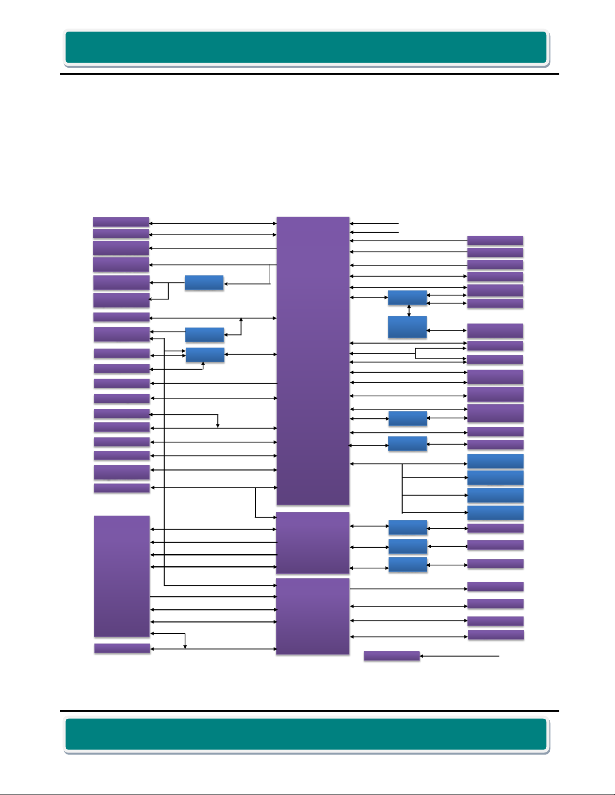
2 Qseven GENERIC CARRIER BOARD DESIGN
This section is designed to provide detailed information about the electrical design and practical
considerations that went into the Qseven Generic Carrier Board. This section is organized to discuss
each block in the following high level block diagram, as shown below.
2.1 Qseven Generic Carrier Board Block Diagram
Figure 1: Qseven Generic Carrier Board Block Diagram
Rev 2.0
Page 12 of 164

Generic Qseven Carrier Board Hardware User Guide
iWave Systems Technologies Pvt. Ltd.
2.2 Qseven Generic Carrier Board Features
Qseven Generic Carrier Board supports the following features to validate Qseven Edge Connector
Interfaces and iWave’s Qseven CPU Module specific Expansion Connector interfaces.
Qseven Edge Connector Features
Serial Interface Features
Debug UART console through DB9 Connector
UART0 header for iWave GPS
Communication Features
10/100/1000 Mbps Ethernet through RJ45MagJack
SDIO Ports
SD/MMC Connector¹
On board Taiyo Yuden SDIO Wi-Fi module “WYSAAVDX7”¹
USB Ports
USB 2.0 Host x 2 Ports through Type-A Stacked Connector
Mini PCIe connector with USB 2.0 Host Interface²
USB 2.0 OTG Port through Mini AB Connector
CAN port1 through DB9 Connector
High Speed Interface Features
SATA
22pin Serial ATA Connector for SATA port0
7pin Serial ATA Connector for SATA port1
PCI Express
4-port PCIe Switch through PCIe Port0
Mini PCIe Connector through PCIe Switch Port1²
PCIe x1 Connector through PCIe Switch Port2
PCIe to USB 3.0 Hub controller through PCIe Switch Port3 for USB 3.0 Host x 2
PCIe Port 2 - SMD Pad Header
PCIe Port 3 - SMD Pad Header
Rev 2.0
Page 13 of 164

Generic Qseven Carrier Board Hardware User Guide
iWave Systems Technologies Pvt. Ltd.
Audio/Video Features
AC’97 Audio Codec with 3.5mm Audio IN/OUT jack
LVDS Display Interface
20pin LVDS0 connector with backlight connector³
7” RGB Resistive Touch LCD³
7” RGB Capacitive Touch LCD³
20pin LVDS1 connector with backlight connector
HDMI port
Additional Features
10-Pin JTAG Connector
RTC Coin cell Holder
Control Buttons
Power On/Off Button
Reset Button
Tamper Switch (Optional)
Sensors
Ambient Light Sensor
Digital eCompass
3-Axis accelerometer
Altimeter/Barometer
Add-on Headers
SPI Header
LPC Header
SDVO Header
Qseven control signal Header
Note:
1. Either 8-bit MMC/SDIO or Wi-Fi Module only can be used at a time.
2. Mini PCIe connector supports both USB interface and PCIe interface.
3. Either LVDS0 connector or 7” RGB resistive LCD or 7” RGB capacitive LCD can be used at a time.
Rev 2.0
Page 14 of 164

Generic Qseven Carrier Board Hardware User Guide
iWave Systems Technologies Pvt. Ltd.
iWave’s Qseven CPU Module specific Expansion Connector Features
UART2 Header
CAN port2 connector
TV-In Composite Video through RCA Jack
8bit CMOS Camera Connector
MIPI Camera Connector
4X4 Keypad Header
TV Out Composite Video Header
VGA Interface Header
120-pin Carrier Board Expansion Connector
General Specification
Power Supply : 12V, 2A Power Input Jack
LED Indicators
Power Indicator Red LEDs
Reset Indicator Red LED
Temperature : 0°C to +60°C
Form Factor : 120mm X 120mm Nano ITX
Rev 2.0
Page 15 of 164
Generic Qseven Carrier Board Hardware User Guide
iWave Systems Technologies Pvt. Ltd.
2.3 Qseven MXM Connector
The Qseven module utilizes a 230-pin board-edge connector that is also used for PCI Express capable
notebook graphics cards following the MXM specification. Therefore this connector type is also known
as MXM connector. The MXM connector (J12) is a robust, low-cost edge connector that is capable of
handling high-speed serialized signals.
Figure 2: Qseven MXM Connector
Rev 2.0
Page 16 of 164

Generic Qseven Carrier Board Hardware User Guide
iWave Systems Technologies Pvt. Ltd.
Pin
No.
Edge Connector
Pin Name
Signal Type
Voltage Level/
Termination
Description
1
GND1
Power
0V
Ground.
2
GND2
Power
0V
Ground.
3
GBE_MDI3-
Input/Output
Differential
Gigabit Ethernet MDI differential pair 3
negative.
4
GBE_MDI2-
Input/Output
Differential
Gigabit Ethernet MDI differential pair 2
negative.
5
GBE_MDI3+
Input/Output
Differential
Gigabit Ethernet MDI differential pair 3
positive.
6
GBE_MDI2+
Input/Output
Differential
Gigabit Ethernet MDI differential pair 2
positive.
7
GBE_LINK100#
Input
3.3V CMOS
100Mbps Ethernet Link status LED.
8
GBE_LINK1000#
Input
3.3V CMOS
Gigabit Ethernet Link status LED.
9
GBE_MDI1-
Input/Output
Differential
Gigabit Ethernet MDI differential pair 1
negative.
10
GBE_MDI0-
Input/Output
Differential
Gigabit Ethernet MDI differential pair 0
negative.
11
GBE_MDI1+
Input/Output
Differential
Gigabit Ethernet MDI differential pair 1
positive.
12
GBE_MDI0+
Input/Output
Differential
Gigabit Ethernet MDI differential pair 0
positive.
13
GBE_LINK#
Input
3.3V CMOS
Gigabit Ethernet Link status LED.
14
GBE_ACT#
Input
3.3V CMOS
Gigabit Ethernet Activity status LED.
15
GBE_CTREF
Power In
3.3V
Reference voltage for Ethernet
magnetic centre tap.
16
SUS_S5#
Input
3.3V CMOS
Soft Off State.
Default NC.
17
WAKE#
Output
3.3V CMOS
External system wake event.
Default NC.
Connected to 8th Pin of Qseven Control
Signal Header (J53) through resistor and
default not populated.
18
SUS_S3#
Input
3.3V CMOS
Suspend to RAM.
Default NC.
Table 2: Qseven MXM Connector Pin Out
Rev 2.0
Page 17 of 164

Generic Qseven Carrier Board Hardware User Guide
iWave Systems Technologies Pvt. Ltd.
19
SUS_STAT#
Input
3.3V CMOS
Suspend Status.
Default NC.
Connected to 3rd Pin of Qseven Control
Signal Header (J53) through resistor and
default not populated.
20
PWRBTN#
Output
3.3V CMOS/
10K Pull-up
Power button.
Connected to push button S1.
21
SLP_BTN#
Output
3.3V CMOS
Sleep button.
Default NC.
Connected to 5th Pin of Qseven Control
Signal Header (J53) through resistor and
default not populated.
22
LID_BTN#
Output
3.3V CMOS
LID Button.
Default NC.
Connected to 6th Pin of Qseven Control
Signal Header (J53) through resistor and
default not populated.
23
GND3
Power
0V
Ground.
24
GND4
Power
0V
Ground.
25
GND5
Power
0V
Ground.
26
PWGIN
Output
5V CMOS/
10K Pull-up
Power good input.
27
BATLOW#
Output
3.3V CMOS
Battery low indication.
Default NC.
Connected to 9th Pin of Qseven Control
Signal Header (J53) through resistor and
default not populated.
28
RSTBTN#
Output
3.3V CMOS
Active low Reset button.
Connected to push button S2.
29
SATA0_TX+
Input
Differential
SATA0 Transmit Input differential
positive.
30
SATA1_TX+
Input
Differential
SATA1 Transmit Input differential
positive.
31
SATA0_TX-
Input
Differential
SATA0 Transmit Input differential
negative.
Rev 2.0
Page 18 of 164
Generic Qseven Carrier Board Hardware User Guide
iWave Systems Technologies Pvt. Ltd.
32
SATA1_TX-
Input
Differential
SATA1 Transmit Input differential
negative.
33
SATA_ACT#
Input
3.3V CMOS
SATA command Activity line.
34
GND6
Power
0V
Ground.
35
SATA0_RX+
Output
Differential
SATA0 Receive Output differential
positive.
36
SATA1_RX+
Output
Differential
SATA1 Receive Output differential
positive.
37
SATA0_RX-
Output
Differential
SATA0 Receive Output differential
negative.
38
SATA1_RX-
Output
Differential
SATA1 Receive Output differential
negative.
39
GND7
Power
0V
Ground.
40
GND8
Power
0V
Ground.
41
BIOS_DISABLE#/
BOOT_ALT#
Output
3.3V CMOS
Default NC.
Connected to 10th Pin of Qseven Control
Signal Header (J53) through resistor and
default not populated.
42
SDIO_CLK#
Input
3.3V CMOS
SD/MMC card clock.
43
SDIO_CD#
Output
3.3V CMOS
SD/MMC card Detect pin.
44
SDIO_LED
Input
3.3V CMOS
SD/MMC card indication LED.
45
SDIO_CMD
Input/Output
3.3V CMOS
SD/MMC card Command line.
46
SDIO_WP
Output
3.3V CMOS
SD/MMC card Write Protect pin.
47
SDIO_PWR#
Input
3.3V CMOS
SD/MMC card Power Enable pin.
48
SDIO_DAT1
Input/Output
3.3V CMOS
SD/MMC card Data Line (Bit1).
49
SDIO_DAT0
Input/Output
3.3V CMOS
SD/MMC card Data Line (Bit0).
50
SDIO_DAT3
Input/Output
3.3V CMOS
SD/MMC card Data Line (Bit3).
51
SDIO_DAT2
Input/Output
3.3V CMOS
SD/MMC card Data Line (Bit2).
52
SDIO_DAT5
Input/Output
3.3V CMOS
SD/MMC card Data Line (Bit5).
53
SDIO_DAT4
Input/Output
3.3V CMOS
SD/MMC card Data Line (Bit4).
54
SDIO_DAT7
Input/Output
3.3V CMOS
SD/MMC card Data Line (Bit7).
55
SDIO_DAT6
Input/Output
3.3V CMOS
SD/MMC card Data Line (Bit6).
56
RSVD1
NC
NC
Default NC.
Connected to 1
st
Pin of Qseven Control
Signal Header (J53) through resistor and
default not populated.
Rev 2.0
Page 19 of 164
Generic Qseven Carrier Board Hardware User Guide
iWave Systems Technologies Pvt. Ltd.
57
GND9
Power
0V
Ground.
58
GND10
Power
0V
Ground.
59
HDA_SYNC/
I2S_WS
Input
3.3V CMOS
Audio Transmit frame synchronization
line.
60
SMB_CLK/
GP1_I2C_CLK
Input
3.3V CMOS
System Management Bus Clock.
61
HDA_RST#/
I2S_RST#
Input
3.3V CMOS
Audio reset.
62
SMB_DAT/
GP1_I2C_DAT
Input/Output
3.3V CMOS
System Management Bus Data.
63
HDA_BITCLK/
I2S_CLK
Input
3.3V CMOS
Audio Transmit Clock line.
64
SMB_ALERT#
Output
3.3V CMOS
System Management Bus Alert input.
Default NC.
Connected to 3rd Pin of SDVO Header
(J47) through resistor and default not
populated.
65
HDA_SDI/ I2S_SDI
Output
3.3V CMOS
Audio Transmit data line.
66
GP0_I2C_CLK
Input
3.3V CMOS/
4.7K Pull-up
I2C Clock signal.
67
HDA_SDO/
I2S_SDO
Input
3.3V CMOS
Audio Receive data line.
68
GP0_I2C_DAT
Input/Output
3.3V CMOS/
4.7K Pull-up
I2C Data signal.
69
THRM#
Output
3.3V CMOS
Thermal Alarm active low signal.
Connected to 11
th
Pin of Qseven Control
Signal Header (J53).
70
WDTRIG#
Output
3.3V CMOS
Watchdog trigger signal.
Default NC.
Connected to 2nd Pin of Qseven Control
Signal Header (J53) through resistor and
default not populated.
71
THRMTRIP#
Input
3.3V CMOS
Thermal Trip indicates an overheating
condition of the Processor.
Connected to 12th Pin of Qseven Control
Signal Header (J53).
Rev 2.0
Page 20 of 164

Generic Qseven Carrier Board Hardware User Guide
iWave Systems Technologies Pvt. Ltd.
72
WDOUT
Input
3.3V CMOS
Watchdog event indicator input.
Default NC.
Connected to 4th Pin of Qseven Control
Signal Header (J53) through resistor and
default not populated.
73
GND11
Power
0V
Ground.
74
GND12
Power
0V
Ground.
75
USB_P7-/
USB_SSTX0-
Input/Output
Differential
USB Host Port7 Data negative.
76
USB_P6-/
USB_SSRX0-
Input/Output
Differential
USB Host Port6 Data negative.
77
USB_P7+/
USB_SSTX0+
Input/Output
Differential
USB Host Port7 Data positive.
78
USB_P6+/
USB_SSRX0+
Input/Output
Differential
USB Host Port6 Data positive.
79
USB_6_7_OC#
Output
3.3V CMOS
Over current sense for USB ports 6 & 7.
Connected to 114th Pin of Carrier board
Expansion connector (J10).
80
USB_4_5_OC#
Output
3.3V CMOS
Over current sense for USB port 4 & 5.
81
USB_P5-/
USB_SSTX1-
Input/Output
Differential
USB Host Port5 Data Negative.
82
USB_P4-/
USB_SSRX1-
Input/Output
Differential
USB Host Port4 Data negative.
83
USB_P5+/
USB_SSTX1+
Input/Output
Differential
USB Host Port5 Data Positive.
84
USB_P4+/
USB_SSRX1+
Input/Output
Differential
USB Host Port4 Data Positive.
85
USB_2_3_OC#
Output
3.3V CMOS
Over current sense for USB port 2 & 3.
86
USB_0_1_OC#
Output
3.3V CMOS
Over current sense for USB port 0 & 1.
87
USB_P3-
Input/Output
Differential
USB Host Port3 Data negative.
88
USB_P2-
Input/Output
Differential
USB Host Port2 Data negative.
89
USB_P3+
Input/Output
Differential
USB Host Port3 Data Positive.
90
USB_P2+
Input/Output
Differential
USB Host Port2 Data Positive.
91
USB_CC
Output
3.3V CMOS
USB client connect.
92
USB_ID
Output
3.3V CMOS
USB OTG ID to identify Host & device.
93
USB_P1-
Input/Output
Differential
USB OTG Data negative.
Rev 2.0
Page 21 of 164

Generic Qseven Carrier Board Hardware User Guide
iWave Systems Technologies Pvt. Ltd.
94
USB_P0-
Input/Output
Differential
USB Host Port0 Data negative.
95
USB_P1+
Input/Output
Differential
USB OTG Data Positive.
96
USB_P0+
Input/Output
Differential
USB Host Port0 Data Positive.
97
GND13
Power
0V
Ground.
98
GND14
Power
0V
Ground.
99
eDP0_TX0+/
LVDS_A0+
Input
LVDS
LVDS primary channel differential pair0
positive.
100
eDP1_TX0+/
LVDS_B0+
Input
LVDS
LVDS secondary channel differential
pair0 positive.
101
eDP0_TX0-/
LVDS_A0-
Input
LVDS
LVDS primary channel differential pair0
negative.
102
eDP1_TX0-/
LVDS_B0-
Input
LVDS
LVDS secondary channel differential
pair0 negative.
103
eDP0_TX1+/
LVDS_A1+
Input
LVDS
LVDS primary channel differential pair1
positive.
104
eDP1_TX1+/
LVDS_B1+
Input
LVDS
LVDS secondary channel differential
pair1 positive.
105
eDP0_TX1-/
LVDS_A1-
Input
LVDS
LVDS primary channel differential pair1
negative.
106
eDP1_TX1-/
LVDS_B1-
Input
LVDS
LVDS secondary channel differential
pair1 negative.
107
eDP0_TX2+/
LVDS_A2+
Input
LVDS
LVDS primary channel differential pair2
positive.
108
eDP1_TX2+/
LVDS_B2+
Input
LVDS
LVDS secondary channel differential
pair2 positive.
109
eDP0_TX2-/
LVDS_A2-
Input
LVDS
LVDS primary channel differential pair2
negative.
110
eDP1_TX2-/
LVDS_B2-
Input
LVDS
LVDS secondary channel differential
pair2 negative.
111
LVDS_PPEN
Input
3.3V CMOS
LVDS LCD panel power enable control.
112
LVDS_BLEN
Input
3.3V CMOS
LVDS LCD panel Backlight enable
control.
113
eDP0_TX3+/
LVDS_A3+
Input
LVDS
LVDS primary channel differential pair3
positive.
114
eDP1_TX3+/
LVDS_B3+
Input
LVDS
LVDS secondary channel differential
pair3 positive.
Rev 2.0
Page 22 of 164

Generic Qseven Carrier Board Hardware User Guide
iWave Systems Technologies Pvt. Ltd.
115
eDP0_TX3-/
LVDS_A3-
Input
LVDS
LVDS primary channel differential pair3
negative.
116
eDP1_TX3-/
LVDS_B3-
Input
LVDS
LVDS secondary channel differential
pair3 negative.
117
GND15
Power
0V
Ground.
118
GND16
Power
0V
Ground.
119
eDP0_AUX+/
LVDS_A_CLK+
Input
LVDS
LVDS primary channel differential clock
positive.
120
eDP1_AUX+/
LVDS_B_CLK+
Input
LVDS
LVDS secondary channel differential
clock positive.
121
eDP0_AUX-/
LVDS_A_CLK-
Input
LVDS
LVDS primary channel differential clock
negative.
122
eDP1_AUX-/
LVDS_B_CLK-
Input
LVDS
LVDS secondary channel differential
clock negative.
123
LVDS_BLT_CTRL/
GP_PWM_OUT0
Input
3.3V CMOS
LVDS LCD Panel backlight brightness
control.
124
GP_1-Wire_Bus
Input/Output
3.3V CMOS
HDMI CEC bus.
125
GP2_I2C_DAT/
LVDS_DID_DAT
Input/Output
3.3V CMOS/
4.7K Pull-up
Display ID DDC data line used for LVDS
flat panel detection.
126
eDP0_HPD#/
LVDS_BLC_DAT
Input/Output
3.3V CMOS/
4.7K Pull-up
Control data signal for external SSC
clock chip.
127
GP2_I2C_CLK/
LVDS_DID_CLK
Input
3.3V CMOS/
4.7K Pull-up
Display ID DDC clock line used for LVDS
flat panel detection.
128
eDP1_HPD#/
LVDS_BLC_CLK
Input
3.3V CMOS/
4.7K Pull-up
Control clock signal for external SSC
clock chip.
129
CAN0_TX
Input
3.3V CMOS
CAN channel one TX line.
130
CAN0_RX
Output
3.3V CMOS
CAN channel one RX line
131
DP_LANE3+/
TMDS_CLK+
Input
TMDS
HDMI differential clock positive.
132
RSVD2
(Differential Pair)
NC
NC
Default NC.
Connected to 2nd Pin of SDVO Header
(J47) through resistor and default not
populated.
133
DP_LANE3-/
TMDS_CLK-
Input
TMDS
HDMI differential clock negative
Rev 2.0
Page 23 of 164
Generic Qseven Carrier Board Hardware User Guide
iWave Systems Technologies Pvt. Ltd.
134
RSVD3
(Differential Pair)
NC
NC
Default NC.
Connected to 4th Pin of SDVO Header
(J47) through resistor and default not
populated.
135
GND17
Power
0V
Ground.
136
GND18
Power
0V
Ground.
137
DP_LANE1+/
TMDS_LANE1+
Input
TMDS
HDMI differential data1 positive.
138
DP_AUX+
Input/Output
TMDS
HDMI differential device control data
positive.
Default NC.
Connected to 6th Pin of SDVO Header
(J47) through resistor and default not
populated.
139
DP_LANE1-/
TMDS_LANE1-
Input
TMDS
HDMI differential data1 negative.
140
DP_AUX-
Input/Output
TMDS
HDMI differential device control data
negative.
Default NC.
Connected to 8th Pin of SDVO Header
(J47) through resistor and default not
populated.
141
GND19
Power
0V
Ground.
142
GND20
Power
0V
Ground.
143
DP_LANE2+/
TMDS_LANE0+
Input
TMDS
HDMI differential data0 positive.
144
RSVD4
(Differential Pair)
Input
TMDS
Default NC.
Connected to 10th Pin of SDVO Header
(J47) through resistor and default not
populated.
145
DP_LANE2-/
TMDS_LANE0-
Input
TMDS
HDMI differential data0 negative.
146
RSVD5
(Differential Pair)
NC
NC
Default NC.
Connected to 12th Pin of SDVO Header
(J47) through resistor and default not
populated.
Rev 2.0
Page 24 of 164
Generic Qseven Carrier Board Hardware User Guide
iWave Systems Technologies Pvt. Ltd.
147
GND21
Power
0V
Ground.
148
GND22
Power
0V
Ground.
149
DP_LANE0+/
TMDS_LANE2+
Input
TMDS
HDMI differential data2 positive.
150
HDMI_CTRL_DAT
Input/Output
3.3V CMOS
I2C2 Data signal.
151
DP_LANE0-/
TMDS_LANE2-
Input
TMDS
HDMI differential data2 negative.
152
HDMI_CTRL_CLK
Input
3.3V CMOS/
4.7K Pull-up
I2C2 Clock signal.
153
DP_HDMI_HPD#
Output
3.3V CMOS
HDMI Hot Plug Detect.
154
RSVD6
NC
NC
Default NC.
Connected to 9th Pin of SDVO Header
(J47) through resistor and default not
populated.
155
PCIE_CLK_REF+
Input
Differential
PCIe differential reference clock
positive.
156
PCIE_WAKE#
Output
3.3V CMOS
PCIe interface wake up signal.
157
PCIE_CLK_REF-
Input
Differential
PCIe differential reference clock
negative.
158
PCIE_RST#
Input
3.3V CMOS
PCIe Reset.
159
GND23
Power
0V
Ground.
160
GND24
Power
0V
Ground.
161
PCIE3_TX+
Input
Differential
PCIe3 differential transmit line positive.
162
PCIE3_RX+
Output
Differential
PCIe3 differential receive line positive.
163
PCIE3_TX-
Input
Differential
PCIe3 differential transmit line negative.
164
PCIE3_RX-
Output
Differential
PCIe3 differential receive line negative.
165
GND25
Power
0V
Ground.
166
GND26
Power
0V
Ground.
167
PCIE2_TX+
Input
Differential
PCIe2 differential transmit line positive.
168
PCIE2_RX+
Output
Differential
PCIe2 differential receive line positive.
169
PCIE2_TX-
Input
Differential
PCIe2 differential transmit line negative.
170
PCIE2_RX-
Output
Differential
PCIe2 differential receive line negative.
171
UART0_TX
Input
3.3V CMOS
UART3 Transmit signal.
172
UART0_RTS#
Input
3.3V CMOS
UART3 RTS signal.
173
PCIE1_TX+
Input
Differential
PCIe1 differential transmit line positive.
174
PCIE1_RX+
Output
Differential
PCIe1 differential receive line positive.
Rev 2.0
Page 25 of 164

Generic Qseven Carrier Board Hardware User Guide
iWave Systems Technologies Pvt. Ltd.
175
PCIE1_TX-
Input
Differential
PCIe1 differential transmit line negative.
176
PCIE1_RX-
Output
Differential
PCIe1 differential receive line negative.
177
UART0_RX
Output
3.3V CMOS
UART3 Receive signal.
178
UART0_CTS#
Output
3.3V CMOS
UART3 CTS signal.
179
PCIE0_TX+
Input
Differential
PCIe0 differential transmit line positive.
180
PCIE0_RX+
Output
Differential
PCIe0 differential receive line positive.
181
PCIE0_TX-
Input
Differential
PCIe0 differential transmit line negative.
182
PCIE0_RX-
Output
Differential
PCIe0 differential receive line negative.
183
GND27
Power
0V
Ground.
184
GND28
Power
0V
Ground
185
LPC_AD0/GPIO0
Input/Output
3.3V CMOS
GPIO.
Connected to Touch Controller interrupt
and to 5th Pin of LPC Header (J34).
186
LPC_AD1/GPIO1
Input/Output
3.3V CMOS
GPIO.
Connected to Digital eCompass
interrupt & 6th Pin of LPC Header (J34).
187
LPC_AD2/GPIO2
Input/Output
3.3V CMOS
GPIO.
Connected to 3-Axis Accelerometer
interrupt & 7th Pin of LPC Header (J34).
188
LPC_AD3/GPIO3
Input/Output
3.3V CMOS
GPIO.
Connected to Ambient Light Sensor
interrupt & 8th Pin of LPC Header (J34).
189
LPC_CLK/GPIO4
Input/Output
3.3V CMOS
GPIO.
Connected to Altimeter/ Barometer
interrupt & 9th Pin of LPC Header (J34).
190
LPC_FRAME#/
GPIO5
Input/Output
3.3V CMOS
GPIO.
Connected to SATA and to 10th Pin of
LPC Header (J34).
191
SERIRQ/GPIO6
Input/Output
3.3V CMOS
GPIO
Connected to MIPI power down signal
and to 11th Pin of LPC Header (J34).
192
LPC_LDRQ#/
GPIO7
Input/Output
3.3V CMOS
GPIO.
Connected to USB power switch and to
12th Pin of LPC Header (J34).
193
VCC_RTC
Power
3V
RTC battery voltage input.
Rev 2.0
Page 26 of 164

Generic Qseven Carrier Board Hardware User Guide
iWave Systems Technologies Pvt. Ltd.
194
SPKR/
GP_PWM_OUT2
Input
3.3V CMOS
PWM used to control the LVDS LCD
Backlight.
195
FAN_TACHOIN/
GP_TIMER_IN
Output
3.3V CMOS
Fan tachometer input.
Default NC.
Connected to 5th Pin of SDVO Header
(J47) through resistor and default not
populated.
196
FAN_PWMOUT/
GP_PWM_OUT1
Input
3.3V CMOS
Fan PWM input.
Default NC.
Connected to 7th Pin of SDVO Header
(J47) through resistor and default not
populated.
197
GND29
Power
0V
Ground.
198
GND30
Power
0V
Ground.
199
SPI_MOSI
Input/Output
3.3V CMOS
SPI Master Out Slave In.
Connected to 4th Pin of SPI Header (J29).
200
SPI_CS0#
Input
3.3V CMOS
SPI chip select 0.
Connected to 1st Pin of SPI Header (J29).
201
SPI_MISO
Input/Output
3.3V CMOS
SPI Master In Slave Out.
Connected to 2nd Pin of SPI Header
(J29).
202
SPI_CS1#
Input
3.3V CMOS
SPI chip select 1.
Connected to 7th Pin of SPI Header (J29).
203
SPI_SCK
Input
3.3V CMOS
SPI clock input.
Connected to 5th Pin of SPI Header (J29).
204
MFG_NC4
Output
3.3V CMOS
JTAG Reset Output.
205
VCC_5V_SB1
Power
5V
Standby Power Supply.
206
VCC_5V_SB2
Power
5V
Standby Power Supply.
207
MFG_NC0
Output
3.3V CMOS
JTAG Test Clock.
208
MFG_NC2
Output
3.3V CMOS
Debug UART RX data line UART2_RXD
(EIM_D27).
209
MFG_NC1
Input
3.3V CMOS
Debug UART TX data line. UART2_TXD
(EIM_D26).
210
MFG_NC3
Output
3.3V CMOS
JTAG Test Mode Select.
211
VCC1
Power
5V
Input Supply Voltage.
212
VCC2
Power
5V
Input Supply Voltage.
Rev 2.0
Page 27 of 164
Generic Qseven Carrier Board Hardware User Guide
iWave Systems Technologies Pvt. Ltd.
213
VCC3
Power
5V
Input Supply Voltage.
214
VCC4
Power
5V
Input Supply Voltage.
215
VCC5
Power
5V
Input Supply Voltage.
216
VCC6
Power
5V
Input Supply Voltage.
217
VCC7
Power
5V
Input Supply Voltage.
218
VCC8
Power
5V
Input Supply Voltage.
219
VCC9
Power
5V
Input Supply Voltage.
220
VCC10
Power
5V
Input Supply Voltage.
221
VCC11
Power
5V
Input Supply Voltage.
222
VCC12
Power
5V
Input Supply Voltage.
223
VCC13
Power
5V
Input Supply Voltage.
224
VCC14
Power
5V
Input Supply Voltage.
225
VCC15
Power
5V
Input Supply Voltage.
226
VCC16
Power
5V
Input Supply Voltage.
227
VCC17
Power
5V
Input Supply Voltage.
228
VCC18
Power
5V
Input Supply Voltage.
229
VCC19
Power
5V
Input Supply Voltage.
230
VCC20
Power
5V
Input Supply Voltage.
Rev 2.0
Page 28 of 164
Generic Qseven Carrier Board Hardware User Guide
iWave Systems Technologies Pvt. Ltd.
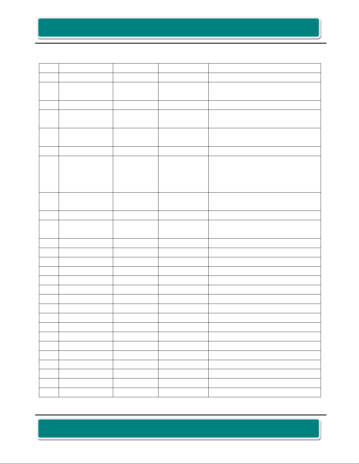
2.4 Serial Interface Features
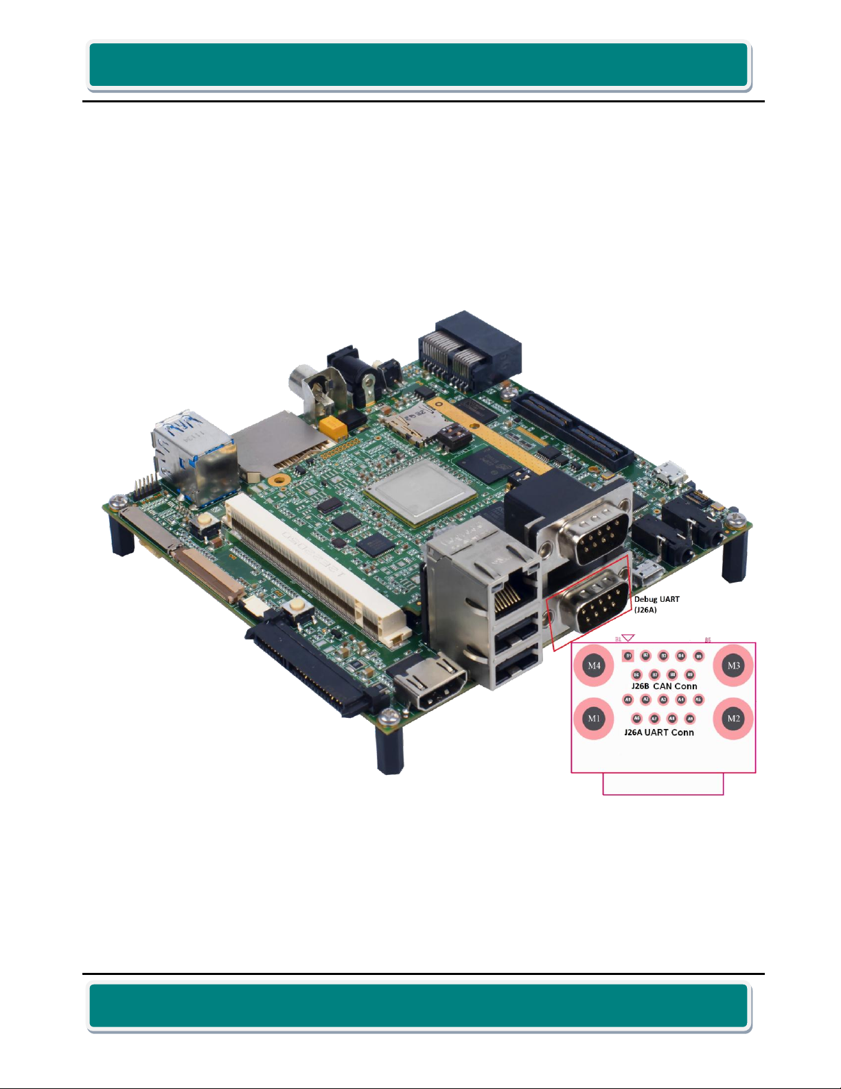
2.4.1 Debug UART console
Debug UART signals from Qseven MXM connector is connected to RS232 Transceiver and to DB9 Male
Debug UART Connector (J26A). This DB9 port can be used for Debug purpose. This is not the full
functional UART and supports only TX and RX signals.
Figure 3: Debug UART Connector
Rev 2.0
Page 29 of 164
Generic Qseven Carrier Board Hardware User Guide
iWave Systems Technologies Pvt. Ltd.
Pin No
Pin Name
Signal Type
Voltage Level/
Termination
Description
A1
NC
NC
NC
NC.
A2
UART_RXD
Input
RS232
Debug UART receive signal.
Connected to 208th Pin of Qseven
MXM Connector through RS232.
Transceiver.
A3
UART_TXD
Output
RS232
Debug UART transmit signal.
Connected to 209th Pin of Qseven
MXM Connector through RS232.
Transceiver.
A4
NC
NC
NC
NC.
A5
GND
Power
0V
Ground.
A6,A7,A8,
A9
NC
NC
NC
NC.
M1,M2,
M3,M4
DSUB_SHLD_GND
Power
0V
Shield Ground.
Table 3: Debug UART Connector Pin Out
2.4.2 UART0 header for iWave GPS
Qseven Generic Carrier Board supports on board UART0 header (J2) through UART0 interface of Qseven
MXM connector. This header can be used to connect iWave’s GPS module and physically located on the
top of the board as shown below.
Number of Pins: 6
Connector Part number: GRPB061VWVN-RC
Mating Connector: LPPB061NFFN-RC from Sullins Connector Solutions
Rev 2.0
Page 30 of 164
 Loading...