

IVO M236MWF2 R0 Specification
InfoVision Optoelectronics (Kunshan)Co., Ltd.
Document Title M236MWF2 R0 Customer Approved Specification Page No. 1/26
Document No. A-M236MWF2-R0-153-02 Issue date 2012/09/27 Revision 00
Customer Approved Specification
To: F-LINK ELECTRONIC CO.,LTD
Product Name: M236MWF2 R0
Document Issue Date: 2012/09/27
Customer InfoVision Optoelectronics
SIGNATURE
SIGNATURE
REVIEWED BY
QA
PREPARED BY
FAE
Please return 1 copy for your confirmation with
your signature and comments.
Note: 1. Please contact InfoVision Company. before designing your product based on this product.
2. The information contained herein is presented merely to indicate the characteristics and
performance of our products. No responsibility is assumed by IVO for any intellectual property
claims or other problems that may result from application based on the module described herein.
FQ-7-30-0-009-03D
Revision
Date Page
Old Description New Description Remark
________________________________________________________________________
All rights strictly reserved reproduction or issue to third parties in any form what ever is not permitted without written authority from the proprietor.
InfoVision Optoelectronics (Kunshan)Co., Ltd.
Document Title M236MWF2 R0 Customer Approved Specification Page No. 2/26
Document No. A-M236MWF2-R0-153-02 Issue date 2012/09/27 Revision 00
00
2012/09/27
- - First issued.
-
________________________________________________________________________
All rights strictly reserved reproduction or issue to third parties in any form what ever is not permitted without written authority from the proprietor.

InfoVision Optoelectronics (Kunshan)Co., Ltd.
Document Title M236MWF2 R0 Customer Approved Specification Page No. 3/26
Document No. A-M236MWF2-R0-153-02 Issue date 2012/09/27 Revision 00
Contents
1. GENERAL DESCRIPTIONS
2. ABSOLUTE MAXIMUM RATINGS
3. ELECTRICAL SPECIFICATION
4. OPTICAL CHARACTERISTICS
5. MECHANICAL CHARACTERISTICS
6. PACKAGE SPECIFICATION
7. LOT MARK
8. GENERAL PRECAUTION
........................................................................................................................................................
...…...….........................................…………………………………………..
...…...….........................................…………………………….....
.........................................................................................................
.......................................................................................................
..........................................................................................
..............................................................................................................
....................................................................................................................
3
6
7
15
18
21
22
23
________________________________________________________________________
All rights strictly reserved reproduction or issue to third parties in any form what ever is not permitted without written authority from the proprietor.
InfoVision Optoelectronics (Kunshan)Co., Ltd.
Document Title M236MWF2 R0 Customer Approved Specification Page No. 4/26
Document No. A-M236MWF2-R0-153-02 Issue date 2012/09/27 Revision 00
1 General Descriptions
1.1 Introduction
The M236MWF2 is a Color Active Matrix Thin Film Transistor (TFT) Liquid Crystal Display
(LCD) module, which uses amorphous Silicon TFT as a switching device. It is composed of a
TFT LCD panel, a timing controller, voltage reference, common voltage, column driver, and row
driver circuit. This TFT LCD has a 23.6 inch (diagonally measured) active display area with
resolution (1,920 vertical by 1,080 horizontal pixel array).
1.2 Features
■ 23.6” TFT LCD Panel
■ LED Backlight System
■ Supports (V:1,920 lines, H:1,080 pixels) Resolution
■ Compatible with RoHS and GP Standard
■ Compatible with TCO 5.0 Standard
1.3 Product Summary
Items Specifications Unit Remark
Screen Diagonal 23.6 inch -
Active Area 521.3x293.2 mm -
Pixels(H x V) 1,920(x3) x1,080 - -
Pixel Pitch 0.2715x0.2715 mm -
Pixel Arrangement R.G.B. Vertical Stripe - -
Display Mode TN Mode, Normally White - -
White Luminance 300 cd/ m
Contrast Ratio 1,000:1 - -
Response Time 5 ms -
View Angle(H/V) 170/160 - -
Input Voltage +5.0 V -
Power Consumption 17.7 Watt -
Module Weight 2,500 (Typ) g -
Outline
Dimension(H x V x D)
Electrical Interface (Logic) 2ch LVDS - -
544.8x320.5x11.9(max) mm -
2
-
Support Color 16.7M - -
NTSC 72 % % -
Optimum Viewing Direction 6 o’clock - -
Surface Treatment AG/3H - -
________________________________________________________________________
All rights strictly reserved reproduction or issue to third parties in any form what ever is not permitted without written authority from the proprietor.
X
LED B/L
InfoVision Optoelectronics (Kunshan)Co., Ltd.
Document Title M236MWF2 R0 Customer Approved Specification Page No. 5/26
Document No. A-M236MWF2-R0-153-02 Issue date 2012/09/27 Revision 00
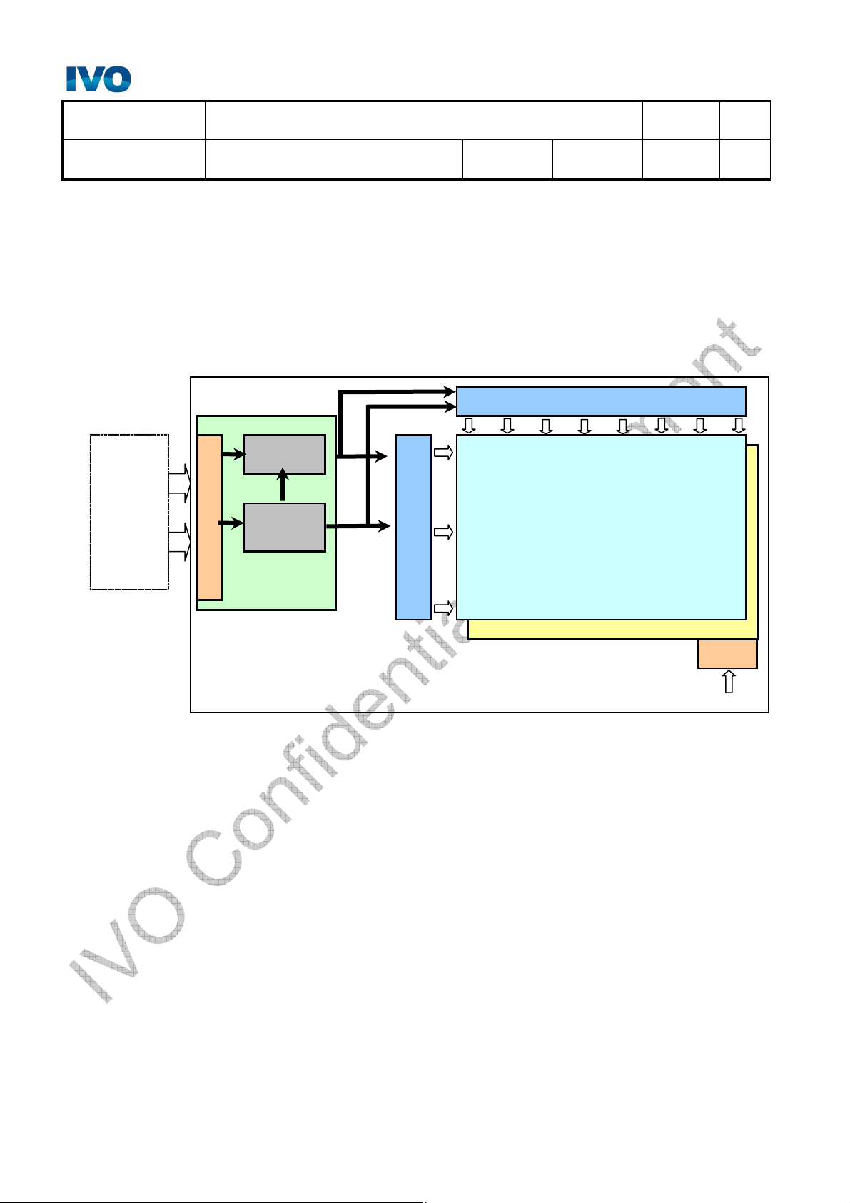
1.4 Functional Block Diagram
Figure 1 shows the functional block diagram of the LCD module.
Figure 1 Block Diagram
VCC
GND
RXinO0+/RXinO1+/RXinO2+/RXinO3+/RXinOC+/RXinE0+/RXinE1+/RXinE2+/RXinE3+/RXinEC+/-
TFT LCD Module
LCD Drive Card
Timing Controller
Connector
DC/DC Converter
Reference Voltage
-Driver
Y-Driver
TFT Array/Cell
1,920(R/G/B) x1,080
Backlight Unit
Connector
________________________________________________________________________
All rights strictly reserved reproduction or issue to third parties in any form what ever is not permitted without written authority from the proprietor.
InfoVision Optoelectronics (Kunshan)Co., Ltd.
Document Title M236MWF2 R0 Customer Approved Specification Page No. 6/26
Document No. A-M236MWF2-R0-153-02 Issue date 2012/09/27 Revision 00
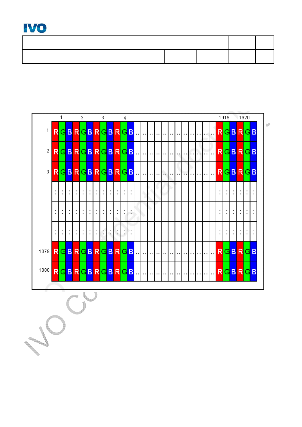
1.5 Pixel Format Image
Figure 2 shows the relationship of the input signals and LCD pixel format image.
Figure 2 Pixel Format
________________________________________________________________________
All rights strictly reserved reproduction or issue to third parties in any form what ever is not permitted without written authority from the proprietor.
InfoVision Optoelectronics (Kunshan)Co., Ltd.
Document Title M236MWF2 R0 Customer Approved Specification Page No. 7/26
Document No. A-M236MWF2-R0-153-02 Issue date 2012/09/27 Revision 00
2
Absolute Maximum Ratings
The followings are maximum values which, if exceeded, may cause faulty operation or damage to
the LCD module.
Table 1
Item Symbol Min.
Supply Voltage VDD -0.3
Input Signal - -0.3
Operating Temperature TOP 0 50
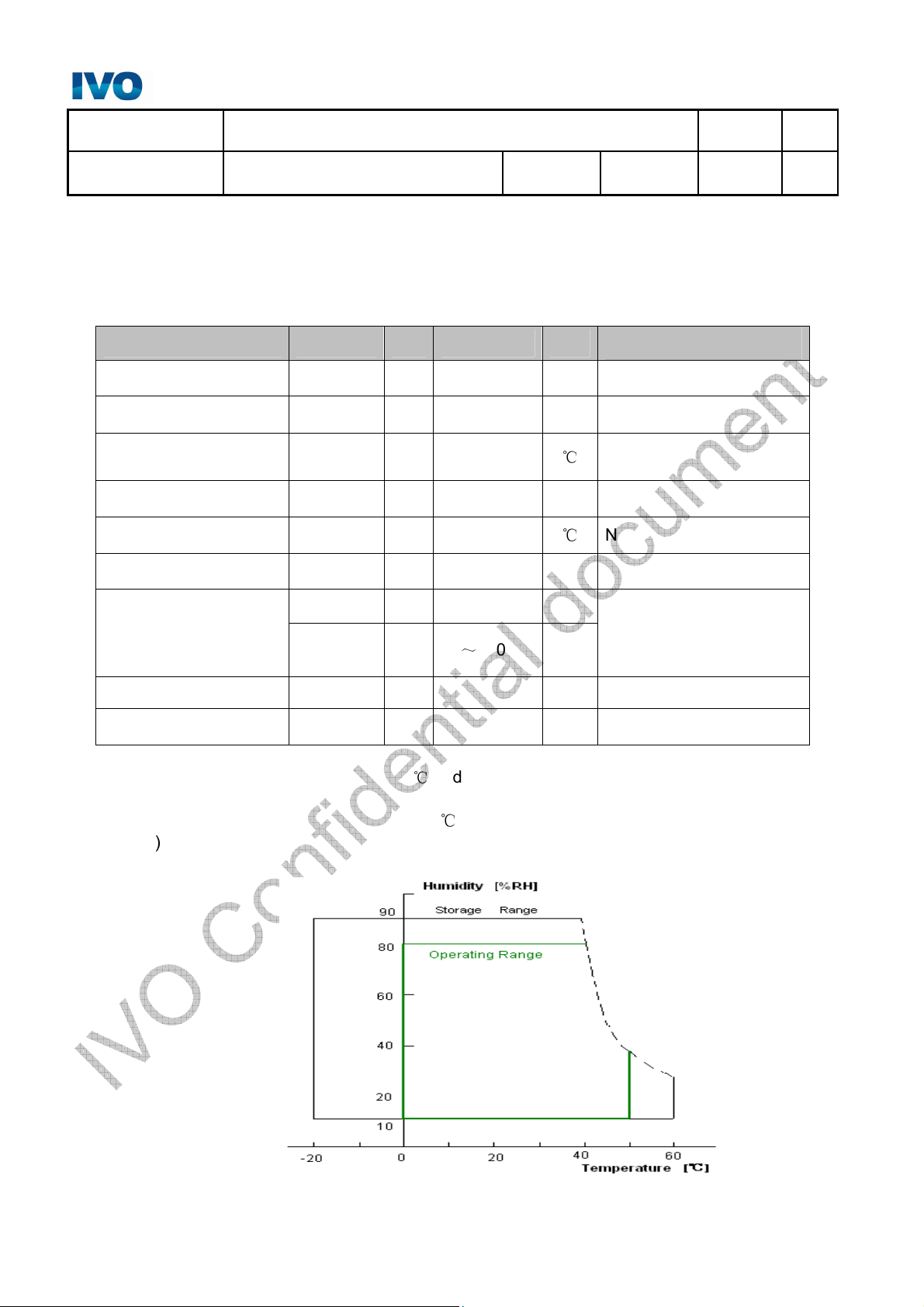
Operating Humidity HOP 10 80 %RH Note(3)
Storage Temperature TST -20
Storage Humidity HST 10 90 %RH Note(3)
Level - 1.5 G
Vibration
Bandwidth - 10~500~10 Hz
Shock Level - 50 G Half sine waveform, 11ms
LED Current I
Note:
(1)Maximum Wet-Bulb should be 39℃ and No condensation
(2)When you apply the LCD module for OA system, please make sure to keep the
temperature of LCD module under 60℃.
(3)Storage /Operating temperature & humidity:
- 60 mA Per LED Chip
_LED
Max. Unit
6.0 V -
2.7 V LVDS Signals
℃
Note(3)
60
℃
Note(3)
30min. for X, Y, Z axis
Conditions
________________________________________________________________________
All rights strictly reserved reproduction or issue to third parties in any form what ever is not permitted without written authority from the proprietor.
LED Light Bar Pin Current
InfoVision Optoelectronics (Kunshan)Co., Ltd.
Document Title M236MWF2 R0 Customer Approved Specification Page No. 8/26
Document No. A-M236MWF2-R0-153-02 Issue date 2012/09/27 Revision 00
3 Electrical Specification
3.1
Electrical Characteristics
Table 2 Electrical Characteristics
Symbol
Parameter Min. Typ. Max. Units
VDD Logic/LCD Drive Voltage 4.5 5.0 5.5
IDD VDD Current - 770 900
PDD VDD Power - 3.9 4.5
Irush Rush Current - - 2.5
Allowable Logic/LCD
VDDrp
- - 300
Drive Ripple Voltage
V
LED Input 25.2 28.8 31.5
_LED
VF LED Forward Voltage 2.8 3.2 3.5
IF LED Forward Current - 60 -
I
PIN
P
LED Power Consumption - 13.8 15.8
LED
LT LED Life Time 30,000
0 120 125
- -
Note:
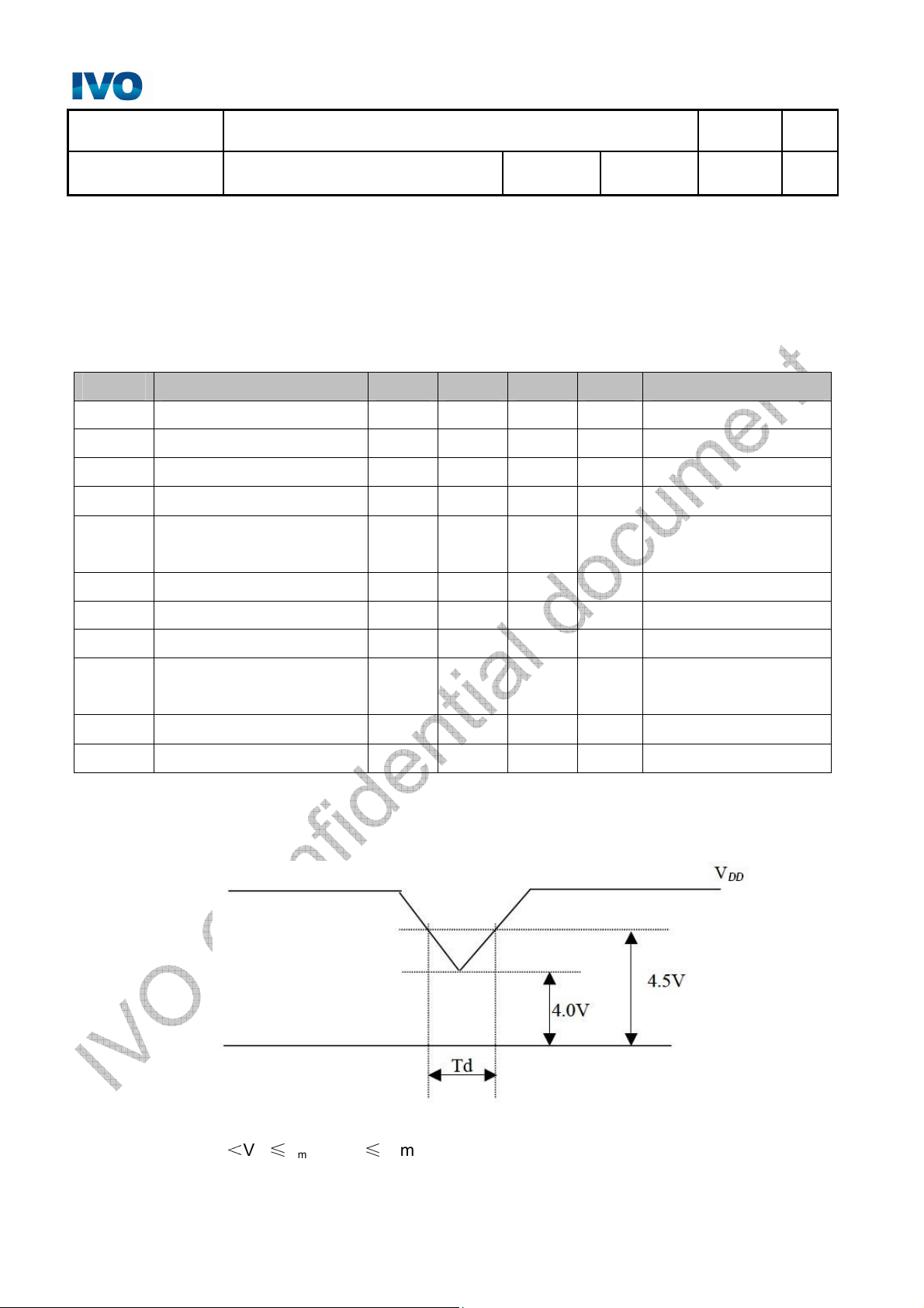
(1)VDD Power Dip Condition
V
mA
W
A
mVp-p
V
V
mA
mA
W
Hours
Condition
Note (1)
Black Pattern, 60Hz
Black Pattern, 60Hz
Note (2)
-
-
-
-
Pin1, Pin2, Pin5 and
Pin6 refer to figure 5.
Note(3)
Note(4)
Figure 3 V
Power Dip
DD
If V
TH
<
V
DD
≤
V
and t
d
≤
min
10ms, our panel must revive automatically when the voltage
returns to normal.
________________________________________________________________________
All rights strictly reserved reproduction or issue to third parties in any form what ever is not permitted without written authority from the proprietor.
 Loading...