

NOILAIHOSHG
TVNOTIDNNÁ
ART
ЗАЛУЛ
dana
OL
SI
20090
8
0/4
τρ
did
OL
8110
Ξ
599807
paras
RL
SNE,
098
YHOLYINSSY
HIMOd
YOOPNTL
02/01
dE
03708
ATNDITO
SIOSI
2247
ЖЗ
О
A
7
ewop
ン
1
011
SAVA
HIATHO
dna
gl
Sk
avos
SEN
000
veses
oF
8
Bros
BEN
a
tod
AS+
9493
AGE
SOWNY/I1901
TOU
INDO
INI
08008
9033-9113
3375713
3718%510
ach
2
E104
oJESTTEA
088-
Foru
T9-€
"4ZZ-€
91NBTA
vezzand
i
osH
ж
5454
AGI
FUNCTIONAL
DESCRIPTION
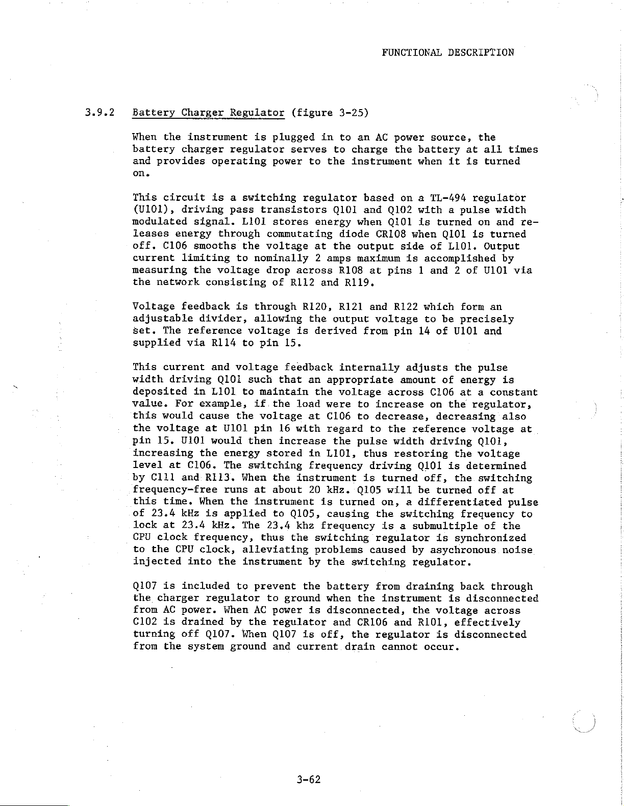
3.9.2
Battery
When
battery
and
Charger
the
instrument
charger
provides
on.
This
modulated
off.
current
measuring
Voltage
adjustable
set.
This
width
deposited
value.
this
pin
level
by
circuit
(0101),
leases
energy
C106
the
network
The
supplied
current
driving
For
would
the
voltage
15.
increasing
at
Cill
driving
signal.
smooths
limiting
the
feedback
divider,
reference
via
in
example,
cause
U101
the
C106.
and.
frequency-free
this
time.
of
23.4
lock
at
CPU
clock
to
the
injected
When
kHz
23.4
frequency,
CPU
clock,
into
Regulator
is
regulator
operating
is a switching
pass
transistors
L101
through
voltage
the
to
nominally
commutating
voltage
drop
consisting
is
through
allowing
voltage
R114
and
L101
Q101
to
pin
voltage
such
to
maintain
if
the
voltage
at
UlOl
pin
would
R113.
is
kHz.
then
energy
The
switching
When
runs
at
the
instrument
applied
The
stored
23.4
thus
alleviating
the
instrument
(figure
plugged
serves
power
regulator
stores
across
of
R112
R120,
is
15.
feedback
that
the
load
16
with
increase
the
instrument
about
to
Q105,
khz
the
3-25)
in
to
to
to
the
0101
energy
diode 08108
at
the
2
amps
R108
and
R119.
R121
the
output
derived
internally
an
appropriate
the
voltage
were
at
C106
regard
the
in
L101,
frequency
20
kHz.
is
turned
causing
frequency
switching
problems
by
the
an
AC
power
charge
instrument
based
and
when
output
maximum
the
battery
when
on a TL-494
0102
with a pulse
0101
when
side
is
at
pins 1 and 2 of
and
R122
voltage
from
pin
adjusts
amount
across
to
increase
to
decrease,
to
the
reference
pulse
Q105
width
thus
restoring
driving
is
turned
will
on, a differentiated
the
Q101
be
switching frequency
is a submultiple
regulator
caused
switching
by
regulator.
source,
it
is
turned
0101
of
L101.
accomplished
which
to
14
form
be
precisely
of
U101
the
of
energy
C106
at a constant
on
the
decreasing
driving
the
is
off,
the
turned
is
synchronized
asychronous
the
at
all
times
is
turned
regulator
width
on
and re-
is
turned
Output
by
UlOl
via
an
and
pulse
is
regulator,
also
voltage
0101,
voltage
determined
switching
off
at
pulse
of
the
noise
at
to
Q107
the
from
C102
is
charger
AC
is
turning
from
the
included
regulator
power.
drained
off
Q107.
system
to
When
by
When
ground
prevent
to
AC
power
the
regulator
Q107
and
the
ground
is
current
3-62
battery
when
is
disconnected,
and
off,
the
drain
from
the
CR106
regulator
draining
instrument
the
and
RIO1,
cannot
is
voltage
is
occur.
back
through
disconnected
across
effectively
disconnected

NOTIAT4DS4G
TVNOTIDNNA
=
AHLINOHTO
cer
oteon
AVASIO
01
À
AHLITOBTO
SOTYNY
OL
I
AULINOUIS
(QdAYY-YT)
BOTYNY
00
AZT+
OL
01
03200
230/80
HBAOd
L
AHALLYS
AMLINOUTO
оно
(<H—————————
ovace
HOLYOTONT
SnLY1S
AS
SINBRnULSNT
NI
NOTO
01408
SSNIHOVA
nddrna3
BALLİ
1904
ALVIS
NT
OL
01
<p
一
v
5
4
91801
(ovos
269
sony
ten)
fer
Ford
save
vasta
va
|
し
TYNTKOK
Зал
ва
Ἠ81ΑΙΙ238
μα
στά
Βοττάάπς
10mog
фо
шел8ета
59-5
NIOTE
‘£7-E
9rnST

FUNCTIONAL
DESCRIPTION
CIRCUIT
120V
=
BREAKER
50/6047
U
ビュ
1
2|
BLK
Figure
|
WHT
O
3-24.
AC
Power
이주
RIS
Connection
5
4
3
ey,
Tt
SECONDARY
3.9.3
CR105
instrument
28
ground
battery
CRLO9
overvoltage
occur
Fuses
Two
tects
the
fuse,
direct
blocks
VDC,
circuits
protects
if
(figure
fuses
against
power
protects
short
the
connected
causing
charger
the
in
case
0101
were
3-25)
are
in
a
distribution
the
to
battery
to
CR106
for
regulator.
fault
ground
U101
battery
of
shorted.
the
battery
to
battery
in
voltage
AC
power,
conduct,
and
and
failure
the
system
and
from
3-64
from
the
biasing
associated
the
rest
of
the
circuit.
power
the
regulator
in
the
associated
battery.
reaching
voltage
circuitry;
of
regulator,
F101, a 2.5 amp
instrument.
C102.
at
C102
0107
on
the
instrument
such
or
somewhere
F102, a 5
circuitry
to
With
reaches
complete
enabling
as
might
fuse,
in
case
the
the
from
pro-
else
amp
of
about
the
in
a
m
NOLIdIXOSIG
tives
TYNOLLONOA
O
vee
tors
.
@
e
©
ANN
SEBO
À
IA
fes
1
г
ne
|
|
1
ー|
=
+
AST
i
|
!
!
;
μπρος
L
R-
7017
80745
ㆍ
sel,
52/0821
(9073
05/001
pr9
||
二
T
>
TOSUN
Hiz
“SOTE
、
'
goro
т
二
ey
AL
mr
yoru!
05/0022]
i
1
Live
438
|
'
4
w/t
M
B-907P
m
i
OA.
OEM
19090
|
q
—_
71
1600
w
"CR
DE
a
o
2617
Яо
ВУ
2118
oje
STESAL
|
PVV
XT/99
2/3
‘08S
8
0874
2358
,
€
Tİ*
|
vues
23
19
JA
19
W
で
909
Mx
JÉ
An
|
|
B
10
Pi
ST),
0003
e
1010
30
ETT
ora,
рых
P
:
иг
$0].
=
y69SENd
ΑΛΑ
СИН
338
XT
NESİP
eğri
vwlorlsjz
23
73
00
cen
yor
1981849
Ate13eg
pue
‘лозеТизен
69-5
9077
*
9T
ユ
す
エコ
9
"σζ-ς
θππ8τῇ
一
、
5
POTN
O/d
ezio
yor
Τρ
|
PİL
asra,
10082
re
n
-rom
91907
AG+
Zoro
>
LESTOS
Г

FUNCTIONAL
DESCRIPTION
3.9.4
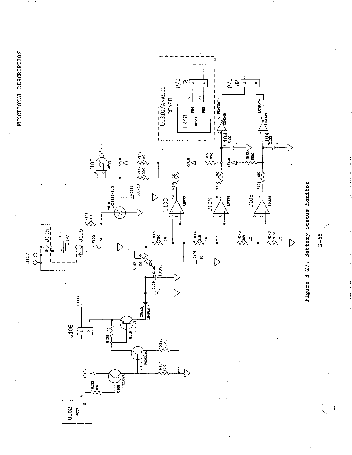
3.9.5
Battery
CR107,
0101
the
Q103
R107,
Charge
0103,
collector,
switching
will
illuminating
thermometer
logic
that
Battery
The
1,
tors.
the
resulting
larly,
LO
the
Status
battery
2,
and
If
junction
if
junction
causing
from
the
voltage
U106
U104 pins 2 and 4 are
logic/analog
at
reference
C115,
ment
setting
(figure
Indicator
C105,
regulator
be
turned
board.
to
port
instrument
Monitor
condition
14.
VRIOl
the
battery
of
in
U106
the
battery
of
R144
pin 2 to
the
junction
voltage.
flip-flop
3-28).
R106,
indicating
on
in
the
charge
This
U40
on
is
operating
(figure
is
provides
voltage
R145
and
pin 1 going
drops
and
R145
go HI
board.
This
(figure
and
C107
that
is
functioning,
this
indicator
also
turns
the
logic/analog
monitored
a
drops
R146
will
HI,
below
will
and
monitored
If
the
of
R143
causes
U103
pins 4 and
3-26)
detect
the
instrument
case,
supplying
on
on
AC
3-27)
by
reference
below
drop
and
11.5
drop
below
U104
pin 2 to
by
voltage
and
R144
U106
pin
the
thus
LED
Q104
board,
power.
three
voltage
11.6
below
U104
volts,
the
the
drops
will
14
10,
switching
is
plugged
charging
current through
on
the
display/
through
R109
signaling
comparators,
to
the
volts,
the
reference
pin 4 going
the
voltage
reference
go
LO.
CPU
through
below
to
drop
go
11.4
below
LO,
disabling
waveform
in
and
the
battery.
to
send
the
U106 pins
compara-
the
voltage
voltage
LO.
Simi-
at
the
voltage
The
signals
port
U40
volts,
the
discharging
the
instru-
at
a
CPU
at
on
the
C115
and
the
pump
summarizes
Table
Battery
Battery
Battery
The
voltage
the
power-on
R147
motor
the
prevent
load,
comparator
3-6.
<
11.6V,
<
11.5V,
<
11.4V,
source
circuit.
short-term
from
Battery
0106-1
U106-2
U106-14
to
the
voltage
turning
reference
Status
Monitor
battery
off
the
thresholds.
=
HI
=
HI
=
LO
status
drops
from,
instrument.
Reference
(i.e.,
(i.e.,
(i.e.,
DEADBAT-
RESET-
monitor
for
Thresholds
LOWBATT-
comes
example,
Table
=
=
=
from
3-6
LO)
LO)
LO)
part
of
3-66
EUNCTIONAL
DESCRIPTION
+5Y
LOGIC
Ri11
40K
P/O
A
FROM
BRIDGE
R107
na
FH407
1441487
€
Ri04 HEAT
33K
CH105
po
ェ
ーー ニ ーー
1
1 i
1
1
1
i
ο
R106
ан
SINK
1
1
7
0102
PN2907A
620/1/2H
1101
А+
08108
insso
8105
2K,
1/24
[+105
220/25
A109-
2.7K
1
C108
A
6108
.25/
해
CHE LED
TO
BATTERY
0101
Bi,
71494
Figure
3-26.
Battery
3-67
Charge
Indicator
NOTLdTHOSHG
1
|
3
1
|
ΕΤ
|
i
1
ITVNOILONNA
し
|
Som
ーー
Ha
e!
一
|
一
一
I
Te
LOT
|
ABT
二
|
sr
no
5
£
gom
5
p
Joe
2034
«E
OYASI
6605
5
Τ-2ΒΡΒΕΝΙ
FOFYA
。
ari
HOT
37/058
μα
7
ansi
的
0/d
SOWNV/9T907_
QHV08
I
|
|
6
8
TH
ve
x
rT
sot
一
en
一
re
seren
1
I
OYASI
BEBK
e
£2
sed
yssea
|
|
tys
srt
Ш
FO
у
Sed
I
자
.
--
1
estu
9010
『
0/d
ee
-1vgovsa
a
238
É
Е
born
ata
T
yoof
ovas
AAA
207
0918
BRENT
2
+
ег
sl
5018
у
=
“ivano
『
5
este
Moor
nov
sm
gorn
【
9
£
κε
2
7001
Av
GEEK
Srta
e259
nus
AOAFUOW
9
ㅁ
3638
181184
x
a
89-5
*/7-Ç
tura
8017
corn
7305
6579
n
Perno
689yNy
o1n8TA
FUNCTIONAL
DESCRIPTION
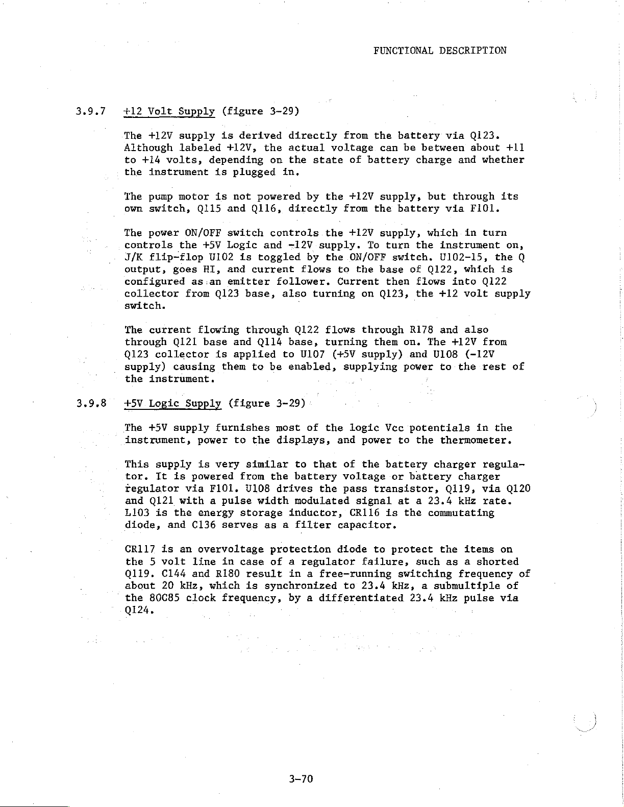
3.9.6
Power
The
an
actuate
U102, a JK
tion,
is
debounce
ON/OFF
off,
On/Off
instrument
electro-mechanical
the
flip-flop,
U102
activated.
is
the
switch
U102
will
the Q output,
the
logic
turning
logic
ing
the
The
+12V
3.9.7
The
LO G output
on,
which
the
battery
divider
status
board
on
the
and
-12V
power
and
and
3.9.8.
then
chain
circuitry
Control
is
turned
electronic
toggled
R128,
ON/OFF
activation.
toggle
pin
14,
through
+12V
power
switch
+5V
power
of
U102
turns
status
comparators,
CR1I13,
is
(figure
on
switch.
switching.
is
the
(changes
R127,
switch
C113
If
so
that
will
J1-10
power
supplies
supply,
again
supplies
is
on
0109
R142,
described
3-28)
or
off
However,
main
and
state)
and
apply
the
control
instrument
the Q output,
go
LO.
The
(PWRON)
which
and
powers
will
reverse
are
applied
and
0110
0106 pins
R143,
in
R144,
section
electronically
a
pushbutton
element.
every
U103-11,
a
time
a
Schmitt
clock pulse
was
pin
high Q output
and
to
the
in
turn
up
the
the
above
discussed
through
to
apply
R145,
R133
1,
further
2,
and
3.9.5
rather
is
In
normal
the
ON/OFF
trigger,
to
U102-13
previously
15,
will
is
base
of
enables
instrument.
process.
in
to
0108,
battery
and
14,
R146.
(figure
than
used
to
switch
turned
go
HI
applied
0122,
the
+5
Actuat-
sections
turning
voltage
through
The
battery
3-27).
with
opera-
upon
and
to
it
to
the
The
battery
are
configured
from
being
voltage
will
go
causing
The
LO
U103
pin 3 to
reset
power
pulls
HI
and
The
CPU
via
output
driving
The
on/off
+5VAO
drops
LO.
U103-4
level
U103-4
source.
U103
U103
can
U103
supply
status
as
circuit
an
toggled
below
This
LO is
and
U103-10
from
U103
go
HI,
and
U103-10,
This
action
pin 8 LO,
pin 4 is
turn
U40
the
port
pin 2 LO,
control
discussed
R/S
to
turn
11.4
volts,
coupled
pin
holding
resetting
LO.
instrument
on
the
causing
circuit
in
can
hold
flip-flop
the
instrument
through
to
be
10
is
U102
the
instrument
turns
U103-4
logic/analog
0103
is
always
section
U102
which
the
battery
set
with
coupled
reset
on
0107,
and
off
by
pin 3 to go
active,
3.9.10.
reset.
can
be
on.
status
R147,
discharging
pin
to
0103
and
the
must
be
pulling
U103-10
resetting
board
and
0103-4
set
to
If
the
output
10
LO
and
pin
instrument
connected
CR112
so
0102. This
turning
HI,
resetting
is
powered
and
prevent
battery
C115
pin 4 HI.
1,
causing
LO,
U103
pin
on
Q106,
0103-10
U102
(U106-14)
and
off.
which
to
is
an
10
done
To
AC
is
U102。
by
the
3-69
FUNCTIONAL
DESCRIPTION
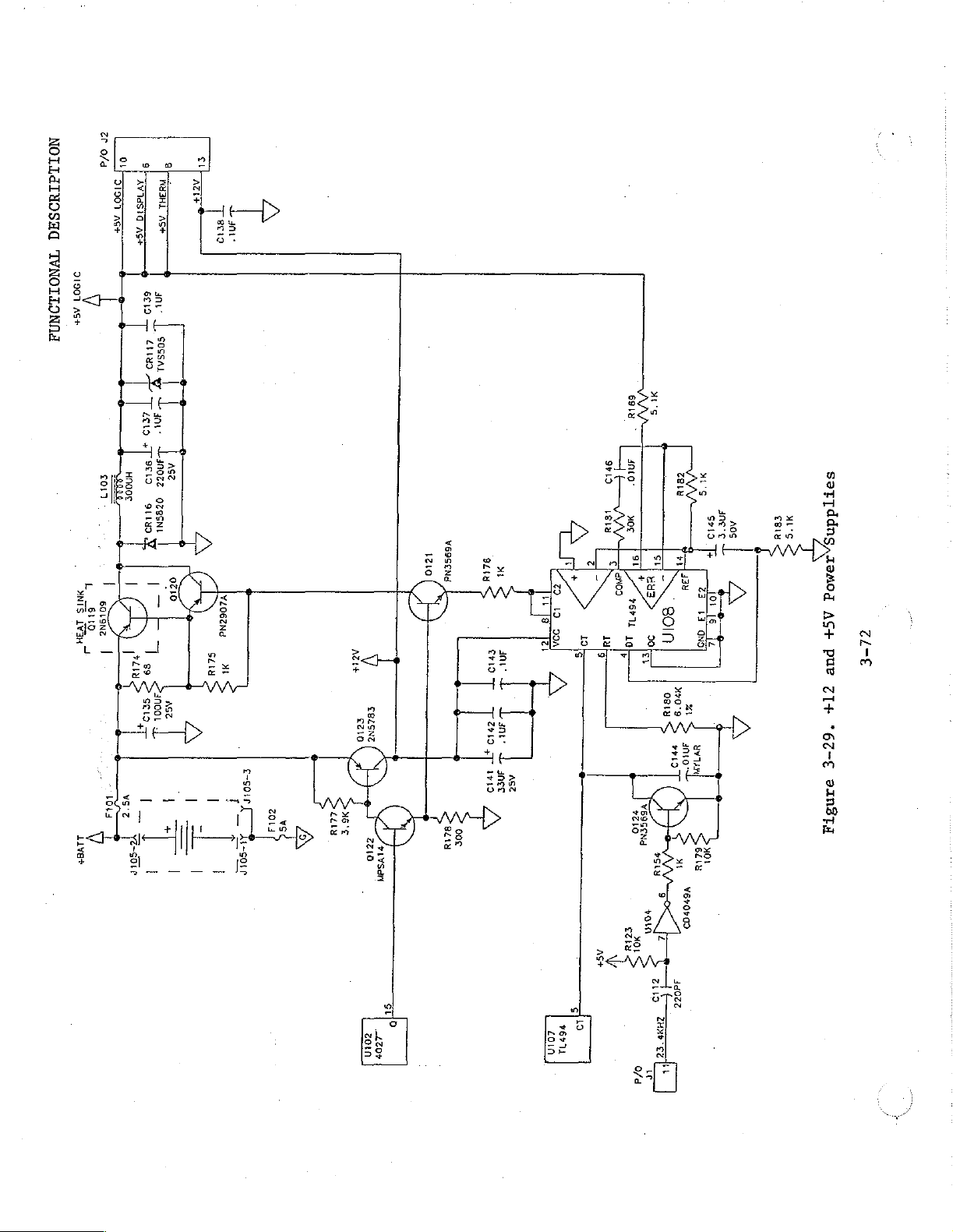
3.9.7
3.9.8
+12
Volt
The
+12V
Although
to
+14
volts,
the
instrument
The
pump
own
switch,
The
power
controls
J/K
flip-flop
output,
configured
collector
switch.
The
current
through
Q123
collector
supply)
the
instrument.
+5V
Logic
Supply
supply
labeled
motor
0115
ON/OFF
the
+5V
goes
HI,
as:an
from
flowing
0121
base
causing
Supply
(figure
is
derived
+12V,
depending
is
plugged
is
not
and
switch
Logic
U102
is
and
emitter
Q123
base,
through
and
is
applied
them
(figure
3-29)
directly
the
actual
on
the
in.
powered
Q116,
directly
controls
and
-12V
toggled
current
follower.
also
Q122
Q114 base,
to
U107
to
be
enabled,
3-29)
state
by
supply.
by
flows
turning
from
voltage
of
the
+12V
from
the
+12V
the
ON/OFF
to
the
Current
flows
turning
(+5V
supplying
the
can
battery
supply,
the
supply,
To
turn
switch,
base
then
on
Q123,
through
them
supply)
battery
be
between
charge
but
battery
which
the
of
Q122,
flows
the
R178
on.
The
and
power
via
0123.
about
and
whether
through
via
F101.
in
turn
instrument
U102-15,
which
into
0122
+12
volt
and
also
+12V
from
U108 (-12V
to
the
rest
+11
its
on,
the
0
is
supply
of
The
+5V
supply
instrument,
This
L103
supply
tor.
It
is
tegulator
and
Q121
is
the
diode,
CR117
the 5 volt
0119.
about
the
and
is
Cl44
20
80085
0124.
furnishes
power
is
powered
via
to
very
from
F101.
with a pulse
energy
C136
an
overvoltage
line
and
kHz,
which
clock
storage
serves
in
case
R180
frequency,
most
the
displays,
similar
the
U108
drives
width
as a filter
protection
of a regulator
result
is
synchronized
by a differentiated
of
the
logic
and
power
to
that
of
the
battery voltage
the
pass
transistor,
modulated
inductor,
signal
CR116
capacitor.
diode
to
failure,
in a free-running
to
23.4
Vcc
potentials
to
the
thermometer.
battery charger
or
battery
at a 23.4
is
the
protect
such
switching
commutating
charger
Q119,
kHz
the
items
as a shorted
frequency
kHz, a submultiple
23.4
kHz
pulse
in
the
regula-
via
rate.
Q120
on
of
of
via
3-70

NOTTATIOSHA
TYNOILONNI
CHIA
s-soin
#7011
{11105
4010
eb
ZL
ibn!
tH
——<
90180
OVAS+
OVAS+
=
EO
6018
OVAS+
Mey
6
A
に
6
IT
στ
вазы
ceor
=
MOL.
aw
gro
=
OVAS+
Agt/anoce
suo
SAR
WL
9
xr
ane
νειο
T
L
8-2
8-vi10
101740)
AJO/NO
14-€
19M0ğd
*87-£
o1N3TA
OVAS+
@ytNt
и
9215
det
30/NO
—p
Sd
0/4
T
+
£
9010
JJONUNL
NOËMd
NOLLdIHOSHA
'IVNOLLONDA
er
o/a
o
Sis
31507
ASF
RET
21901
δει
AS+
‘
—
|
|
2
T
του
EDAŞ
anv
SOSSAL
yy,
ao
al
|
L
ει
AZIK
T“
anı”
xs
6918
.
LHO
2NIS
1V3R
y
divat
*
μησος
91189
sei
219,
Lis
40000
OZESNL
|
gio
b
—
£037
92990
6
l'a
|
ve
wre
|
y
tar
f
」
λατ
1
7
|
4740
9513
E
1618
sog
A
CRLSNZ
сло
£-soir
|
|
Г
一
soir
一
2014
vs
一
I
i
418
M6'£
|-
2210
4
1YSAN
Ve9SENd
1210
ú
actu
ρος
La
»
tro
sud
T
po
La.
Tiro
anes
AGZ
60
fr
19
je
994
je
A
.
19
y
Lie
で
(Oo
[마리
у
[9
56571
10
=>
po
3
8010
oo
gi
0818
V69SENd
velo
AA
sola
Zale
KR
Sal
=
23
1
OND
019
“
%
©
anto”
UYUM
yiz
Situ
Y6y0y02
,
de
$215
で
L
T+
los
fs
--
İz
p-
9
vor
λος
/
A
cel
serrddng
MUŞ
1804
AG+
21-6
PUB
{1+
"62-5
o1N8TA
01
34027
TE
|
sr
40%
dom
76571
4010
d
o.
vel
¡0
|
3.9.9
-12
Volt
The
-12V
analog
or
battery
Supply
supply
circuitry
charger
(figure
is
used
in
the
regulator
3-30)
to
supply
instrument.
via
negative
It
F101.
FUNCTIONAL
bias
is
powered
DESCRIPTION
voltages
from
for the
the
battery
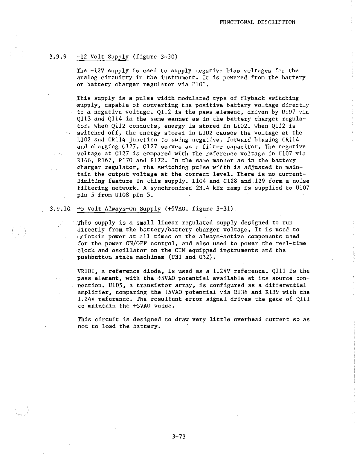
3.9.10
This
supply,
supply
capable
is a pulse width
of
converting
to a negative voltage.
0113
switched
L102
and
voltage
R166, R167, R170
pin 5 from U108
+5
maintain
and
tor.
When
and
charging
charger
tain
the
limiting
filtering
Volt
This
supply
directly
for
the
clock
and
pushbutton
0114
in
Q112
off,
the
CR114
C127.
at
C127
regulator,
output
feature
network.
Always-On
is a smali
from
power
power
the
ON/OFF
oscillator
state
the
conducts,
energy
junction
C127
is
compared
and
the
voltage
in
A
pin
Supply
battery/battery
at
all
machines
Q112
same
is
manner
energy
stored
to
swing
serves
with
R172.
this
In
switching
at
the
supply.
synchronized
5.
(+5VAO,
linear
times
control,
on
the
on
CIM
(U31
modulated
the
positive
the
pass
as
in
is
stored
in
L102
negative,
as a filter
the
the
same
pulse
correct
L104
23.4
figure
regulated
charger
the
always-active
and
also
equipped
and
U32).
type
battery voltage
element,
the
battery
in
causes
forward biasing
capacitor.
reference
manner
width
level.
and
C128
kHz
ramp
3-31)
supply
voltage.
used
instruments
of
flyback
L102.
the
voltage
as
is
There
and
designed
to
power
driven
charger
When
voltage
in
the
adjusted
is no
129
is
supplied
It
components
the
and
switching
directly
by
U107
regula-
Q112
is
at
the
CR114
The
negative
in
U107
via
battery
to
main-
current-
form a noise
to
U107
to
run
is
used
to
used
real-time
the
via
VR101,
pass
nection.
a
element,
amplifier,
1.24V
to
This
not
reference.
maintain
circuit
to
load
reference
with
U105,
a
comparing
the
is
the
diode,
the
transistor
the
The
resultant
+5VAO
designed
battery.
+5VAO
+5VAO
value.
to
is
used
potential available
array,
as a 1.24V
is
configured
potential
error
draw very
'
signal drives
little
3-73
via
reference.
at
its
as a differential
R138
and
R139
the
overhead
current
0111
source
gate
is
with
оЁ
con-
0111
so
the
the
as

FUNCTIONAL
DESCRIPTION
3.10
3.10.1
3.10.2
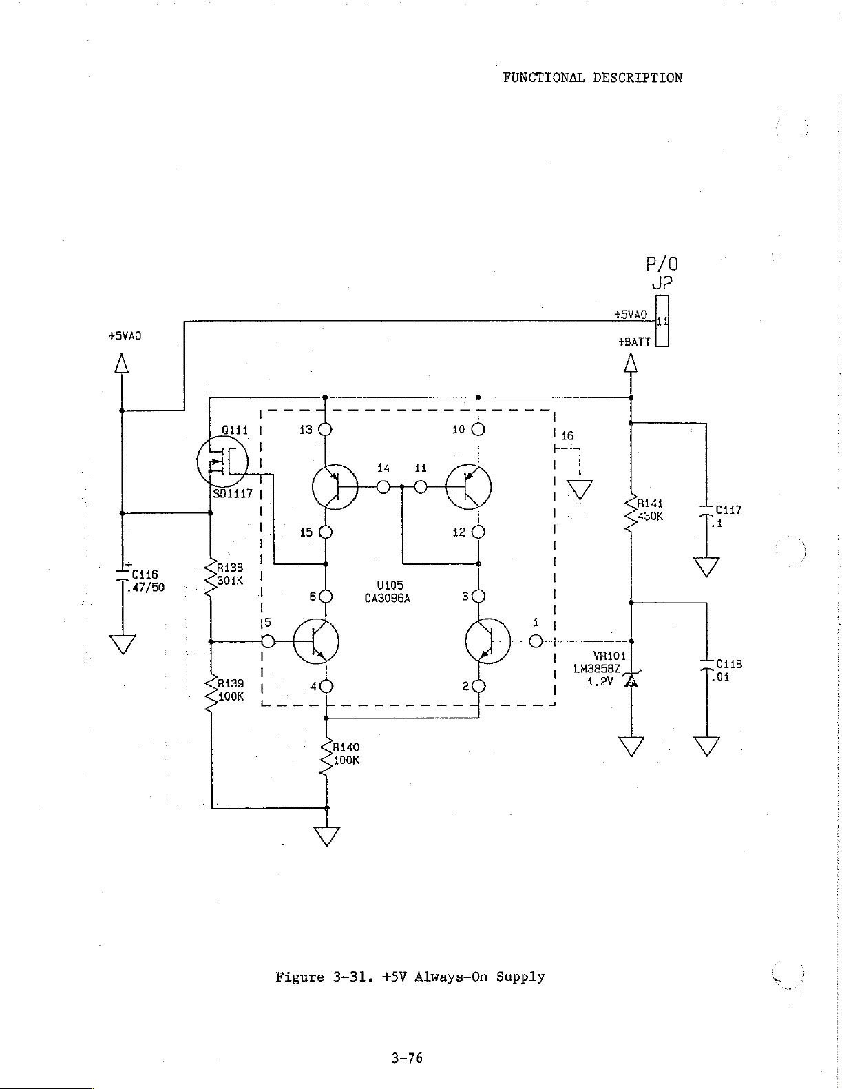
THERMOMETER
Temperature
The
display/thermometer
ing
system,
vated
Measurement
analog
signal
BCD
ler
As
signal
the
display.
circuit
uController
The
2K
timing
writing.
by
removal
temperature
conditioning
words
to
compute
shown
data
in
is
through
The
so
ucontroller
bytes
of
registers,
FUNCTIONS
Measurement
containing
cycle
by
the
and
the
block
linearized
thermometer
that
internal
(Ul,
(UL)
ROM,
(figure
of
the
is
initiated.
signal
circuitry
A/D
converter.
display
diagram
and
the
multiplexer,
figure
is
128
bytes
and
I/O
board
its
own
thermometer
to
the
the
converted
module
power
3-33)
an
NSC
of
porting
3-32)
is
an
essentially
hardware
probe
The
thermometer
module.
and
is
digitized
This data
temperature,
(figure
also
on
COP444L
RAM,
to
and
contains
the
an
for
3-32)
BCD.
writes
board
internal
data
and
software.
from
The
signal
is
used
the
The
the
is
customized
acquisition
independent
its
socket,
probe
is
into
groups
by
analog
ucontroller
temperature
a
power
off
when
IC.
clock
measur-
Once
acti-
a
sends
an
processed
of
the
ucontrol-
temperature
reads
to
control
not
in
It
contains
generator,
and
display
by
three
the
use.
The
ucontroller
the
A/D
display
to
process
In
addition,
speaker
MONITOR
the
DISPLAY
converter
driver
data.
the
(LS1),
mode
switch,
TEST
reads
and
board.
ucontroller
and
reads
the
switch.
and
processes
writes
temperature
Self-contained
operates
and
processes
S2
internal
digital
display
software
the
settings
DIP
temperature
data
to
uses
four
display/thermometer
of
the
NORMAL/
switch
no. 5 (°F/°C),
data
from
the
bit-words
board
and
3-74

NOTT4TADSHG
TYNOLLONDA
0/d
一
>
Lives
ep
а
Fois
E
р
I I
+.
2-5010
1
-
:
S
E
一
5
а
pero
10°
g8rH
u
3065
T
|
=
PAN
17100
4049
TY
|
2071
QESPNT
0209
57914
VETO,
3-2210
e-sorr
ALEL,
I I Ι
1
_
1-50r0
I
1
m
> o
obi
TF
.
80m
vers
ロッ
20
19
CRE
904
5779
Sl
rua
ok
AVS
S814
3006
6218
=
9н09
10
18
tø
+
ὅτι
2443
.
20
E
алых
М>
он
“Téz/or
L
W
>
LOL
ls
se
x
yoz
x
ее
+
€
434
,
|
PETIT
iL
AE
оно
ЯР
199
ver
23
torte
13
OND
le
ATddns
A
AZI-
54-8
‘0£-E
9απΏτά
o
FUNCTIONAL
DESCRIPTION
P/0
Je
+5VA0
+
76116
„47/50
Ly
i
$61117
AA
へ
1 I
8131
|
I
1
CA3096A
A140
400K
ΑΛΑ’
U105
100
14
42
3
146
上 一 一
|
|
|
1
I
!
I
I
I
!
+5V40
La
|,
+BATT
pias
Sul
|,
A
L
τας
4
teus
0
Figure
3-31.
+5V
3-76
Always-On
Supply
NOT
7"T49S4Q
TYNOILONNA
HBMY3JS
suaatua
1N3H935
fy
4
NINO
AYIdSIO
q
BHATBO
11910
HOSS390Hd
08924
.
IL
83x3nd
17930
し
|“
v
у
HOLIMS
Ν/Ν
a
NOTLONAS
HOLIMS
2/96
1937138
A
o
a
κ)
7081N09
ie
Jajawmowleyy,
AlddNS
AMddnS
907YNY
91901
ey]
то
шел8ета
[1-6
яэотя
a0
WNY
83ald3aANO
7011910
90]VNY
o
№
dazTHy3NI]
SONY
inant
any
№
|,
38080
183:
ΑΥΊά5Ι6
dWai
HOSSAD0Hd
HOLINOW
0H9IN
μου”
“da
*25-6
элп8тТя
A
1
1
1
1
FROM
FROM
FROM
6
953
cre
944348
R64
[2
|
R63
47K
。
τος
U8-10
TO
620
CRE
200K
+
9
7
LAN
ve
1
1N4148'
R44
NAV
47K
FUNCTIONAL
DE $ 061
DC
060
255
ους
sl
3
1
]
3
시
T
“CR9
ς
481
JB2
&
sl,
28
27
25]
16
42-4
19
20
37
21
zle
2
094
064
US
cor
서서
po
οι
22
03
si
so
μ7
1No
INT
ΝΣ
INS
co
62
3
RST
GND
7
TA
68
56061
pen
CLKO
curi
vec
-01
2
3
R20
M
Ros
1M
.
EE
|
Yi
R45
2.2k
em
겨서
р
2.0042
cio
je
18pf
DESCRIPTION
962
PN2222A|
-
A
cr
104148
V
УР
+
151
Figure
R14
3-33.
100K
——
vp
Thermometer
3-78
uController
1
The
thermometer
ing
temperature
processing
which
a
is
measurement
CPU.
The
ucontroller
by
used
ucontroller,
and
controlling
the
CPU.
to
turn
cycle,
is
configured
the
and
Only
the
thermometer
display
US,
is
the
thermometer
test
as
follows:
FUNCTIONAL
an
independent
temperature
probe
board
on
command
display
at
is
received
DESCRIPTION
system,
without
sense
the
signal,
beginning
measur-
from
of
the
Inputs
of
NSD,
INO
multiplexer
and
The G port
an
output
through
through
which
off
completed
is
via
Serial
the
CLKO
which
resets
of
the
an
input
the
1/0
speaker
and
utilizes
A3),
B3),
CPU;
establish
internally
time
of
the
routines
proper
rate.
through
MSD),
(GO
which
or
to
the
thermometer
or
the
which
G3
register
to
CLK1
the
divided
ucontroller.
of
the
U9
regarding
and
through
selects
digit
be
power
probe
senses
is
be
activated
are
the
a
2.00
load
programs
IN3
receive
display
G3)
the
strobe
read
an
SO
at
control
when
is.
input
is
external
MHz
for
the
by
32
data from
temperature,
test
has
both
multiplexer
and
the
U5 IN
flip-flop
a
temperature
inserted
the
state
used
an
output
when
inputs.for
crystal.
crystal.
to
achieve
This
cycle
within
-
state
inputs
display
into
of
for
that
it
conducts.
Capacitors
The
the
time
the
ucontroller
DO
digit
(on
channel,
test
port.
for
the
the
testing
turns
crystal
16
ensures
through
strobe
or
off)
and
outputs.
data
state
Gl
is
an
automatic
measurement
storage
probe
the
sense
purposes.
on
clock
C10
frequency
microsecond
that
execute
D3
(LSD,
via
U9-13.
(AO
(BO
output
is
well.
signal
Q62,
generator,
and
Cll
the
outputs
GO
is
turn-
G2
causing
is
cycle
at
the
RST
input,
tion.
Outputs
DO
through
display
with
LO
through
D3
decimal
C8
and
point
and
L6
L7
R14
are
are
is
3-79
performs
the
the
display
driven
display
from
the
segment
digit
output
power-on
drivers.
SK.
initializa-
drivers.
The
Outputs
FUNCTIONAL
DESCRIPTION
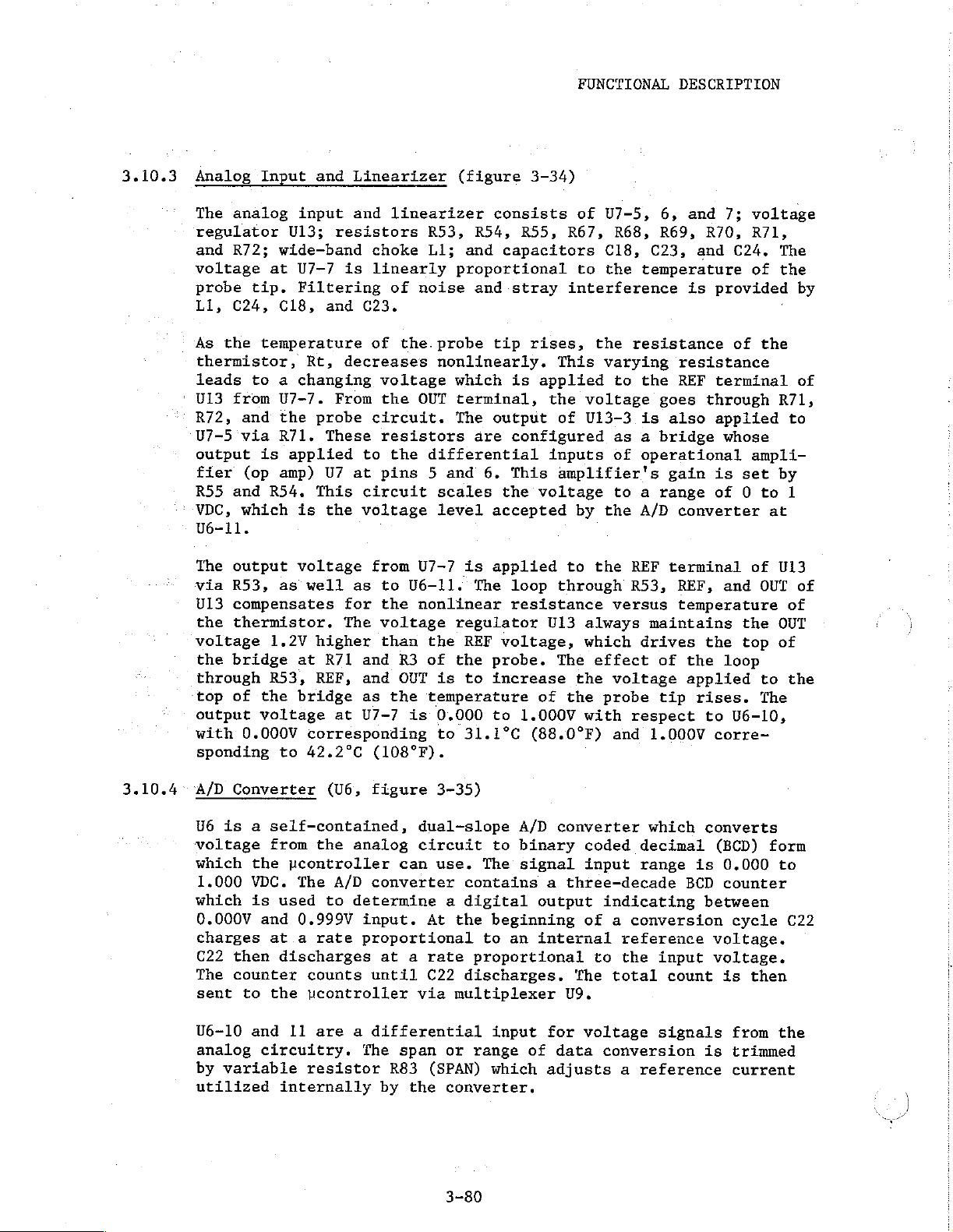
3.10.3
Analog
The
analog
regulator
and
R72;
voltage
probe
Li,
C24,
As
the
thermistor,
leads
U13
from
R72,
U7-5
via
output
fier
R55
and
‘-VDC,
which
U6-11.
The
output
via
R53,
Ul3
compensates
the
thermistor.
voltage
the
bridge
through
top
of
output
with
sponding
Input
and
input
U13;
wide-band
at
U7-7
tip.
Filtering
C18,
and
temperature
Rt,
to a changing
U7-7.
and
the
probe
R71.
These
is
applied
(op
amp)
U7
R54.
This
is
the
voltage
as
well
1.2V
higher
at
R71
R53,
REF,
the
bridge
voltage
0.000V
corresponding
to
42.2°C
Linearizer
and
resistors
choke
is
linearly
C23.
of
decreases
voltage
From
the
circuit.
resistors
to
at
pins 5 and
circuit
voltage
from
as to
for the
The
voltage
than
and
and
as
at
U7-7
(108°F).
(figure
linearizer
R53,
Ll;
proportional
of
noise
the.
probe
nonlinearly.
which
OUT
terminal,
The
the
differential
scales
level
U7-7
U6-11.
nonlinear
regulator
the
R3
of
the
OUT
is
the
temperature
is
0.000
to
consists
R54,
and
capacitors
and
tip
output
are
6.
the
accepted
is
applied
The
REF
voltage,
probe.
to
increase
to
31.1°C
3-34)
R55, R67,
stray
is
configured
This
interference
rises,
This
applied
the
of
inputs
amplifier's
voltage
to
loop
through
resistance
U13
The
of
the
1.000V
(88.0°F)
of
U7-5,
R68,
C18,
to
the
the
varying
to
voltage
Ui3-3
as a bridge
of
to a range
by
the
the
versus
always
which
effect
the
voltage
probe
with
and
6,
and
R69,
C23,
and
temperature
is
resistance
resistance
the
REF
goes
is
also
operational
gain
A/D
converter
REF
terminal
R53,
REF,
temperature
maintains
drives
of
the
applied
tip
rises.
respect
1.000V
7;
voltage
R70, R71,
C24.
of
provided
of
the
terminal
through
applied
whose
ampli-
is
set
of 0 to
at
of
and OUT
the
the
top
loop
to
The
to
U6-10,
corre-
The
the
by
'
of
R71,
to
by
1
U13
of
of
OUT
of
the
3.10.4
A/D
Converter
U6
is a self-contained,
voltage
which
1.000
which
0.000V
charges
C22
The
sent
U6-10
analog
by
utilized
from
the
VDC.
is
and
at a rate
then
counter
to
the
and
circuitry.
variable
ucontroller
The A/D
used
0.999V
discharges
counts
ucontroller
11
resistor
internally
(U6,
figure
the
analog
converter
to
determine
input.
proportional
at a rate
until
are a differential
The
R83
by
3-35)
dual-slope
circuit
can
use.
a
At
C22
via
span
or
(SPAN)
the
converter.
3-80
A/D
to
binary
The
signal
contains
digital
the
beginning
to
an
proportional
discharges.
multiplexer
input
range
which
converter
a
three-decade
output
internal
U9.
for
of
data
adjusts
which
coded
input
decimal
range
indicating
of a conversion
reference
to
the
input
The
total
voltage
count
signals
conversion
a
reference
converts
(BCD)
is
BCD
between
voltage.
voltage.
is
0.000
counter
cycle
is
then
from
trimmed
current
form
to
C22
the
NO77TIJDSAT
WLISI0/D207WNV
3183ANOO
5η
+NI
29%
-NI
TIVNOLLONDE
YA
ino
NI
EM
asso]
ea
Len
FT
sou
|
ーーー
ーー
—
个
nz
2%
,
0/d
」
|
SOTWNY/91907
o/d
00008
o/a
|
|
|
“Lys
ach
SOU
17
ola
oes
woe
128
]
worms
sau
<3
ir
zz
|
|
!
|
|
oP
гг
|
FS
1
|
|
mo
|
|
,
o
ta
|
δρ
6
I
11
.—
—
—
ーー
|
l
I
3
ря
|
23
oz
|
oz
|
|
<
|
a
en
-
$
—
tol
A
3]
ww
ment
τιν
ἱ
{
|
|
|
|
]
869
le
|
|
|
|
|
vi
.
|
|
|
와
v5
#3
eL
|
|
|
|
at
|
|
|
4
|
|
A
<
|
1
I
|
|
80193NNOO
VBNVd
380dd
LNOYS
0/d
19ZT189UT7
pue
2ndu]
18-5
SoTeuy
*YE€-£€
07
ㅁ
897

NOLLATUISAG
"IVNOILONDA
|
189
T
89%
UL
yozz
ANN
998
.
|
eso
Liven
|
|
|
|
|
ovn
vol
si
|
16310
ει
VesZe
zz
a
I
AS+
A
9071VNY/9
02709
19071
o/a
>
i
I
|
|
è
våd
ves
+
©
|
|
|
했
0/4
|
|
wor
I
|
m
|
ze
Le
30
se
st
ou
wey’
I2X9TdFATNN
PUB
ptyNi
919
¥
da
da
ANN
x00z
+94
V
a
|
£a
Veto
sn
409
INI
ET
6
i
#7]
00
19
4520403
6N
cv
γι
은
an
OZ
pee
zi
5
čo
zv
더
ent
09
Le
τις
a/v
x
ον
[5
T
P
|
200
ua
0432
IN
0832
pay
ED
an
zi
Ly
dva
8
z
z91evo
ANO:
s
i
I
fp
zn
u“
es
519$"
054
NI
οι
NIV9
si
seu
©
e
9
©
NYdS
vol
ㅣ
ーー
VA
08032”
し
+
I
£
6
yos
seu
Ie37TBAUOD
28-€
G/V
*GE€-£
элозтя
1
I
198
AVIS!
dS
id
JSAL
The
zero
adjust
analog circuit
zero.
R84
(ZERO)
adjusted.
The
voltage
2,
4,
is
it is
and | outputs
equivalent
the
significant
[MSD]),
3,
and
The
digits
the
temperature
represents
Every value
107.9°F.
temperature
MSD,
U6
NSD,
operates
conversion.
is
4).
The
level
ones
digit
indicated
do
107.9°F,
from
reading,
and
continuously
circuit
is
zero
is a variable
is
coded
of
to
one
raw
(least
[NSD]),
by
not
indicate
data.
the
000
to
ucontroller
The
LSD
digit
of
U6
volts,
in
U6
(U6-16,
digit
significant
or
the
the
LSD,
the
For
example,
top
and
999
represents
converts
digits
strobes,
at a rate
ensures
the
digital
resistor
three
15,
of
the
digit
hundreds
NSD,
actual
bottom
this
are
indicating
of
FUNCTIONAL
that
output
which
four-bit
1,
and
temperature
[LSD]),
(most
and
MSD
temperature,
000
represents
of
the
a
temperature
raw
output
about
DESCRIPTION
when
can
data
2).
the
of
Each
input
U6 is
be
words
reading.
the
significant
outputs
but
88.0°F
temperature
value
to
sequentially
which
9.5
digit
milliseconds
manually
at
four-bit
tens
(next
of U6
represent
and
from
the
actual
with
is
from
the
also
the
8,
word
Whether
digit
(U6-5,
999
range.
88.0°F
the
present.
per
to
3.10.5
Multiplexer
The
multiplexer
and
display
of
four-bit
Inputs
BO-B3
state.
AO-A3
(U9-3,
AQ
output;
receives
from
the
BO-B3
The
which
outputs
when
controlled
The
R63.
outputs
to
are
multiplexer
four-bit
SEL
OE
input
It
facilitate
(U9,
figure
accepts
test
data
receives
A2
from
data
NSD
two
DO
through
is
by
can
in a high-impedance
(U9-2,
6,
10,
the
from
output.
distinct
select
word,
LO;
the B word
the
of
the
be
driven
signal.
words
5,
and
data
"4"
the
B3
A
D3
GO
output
multiplexer
(U9-4,
HI
testing.
3-35)
digital
Output
at
DO-D3,
11,
and
13)
are
from
output;
MSD
output
receives
four-bit
(SEL),
or
B,
is
of
by
test
state.
information
is
14)
digit
the
"1"
and
the
words.
at
U9-1,
is
sent
7,
9,
selected
the
(U9-15)
equipment
to
the:
are
temperature
strobes
output
АЗ
from
of
U6;
display
acts
to
the
and
12).
when
ucontroller
is
This
allows
from
ucontroller
and
of
U6;
the
Bi
from
test
as a switch
ucontroller
The A word
SEL
(U5-21).
normally.
to
put
simulation
the
the
"8"
the
state.
is
the
A/D
converter
in
the
data.
Inputs
display
Al
from
output.
LSD
output;
A0-A3
to
through
is
HI,
SEL
pulled
multiplexer's
of
form
test
the
"2"
BO
and
pick
selected
is
down
data
B2
by
3-83
FUNCTIONAL
DESCRIPTION
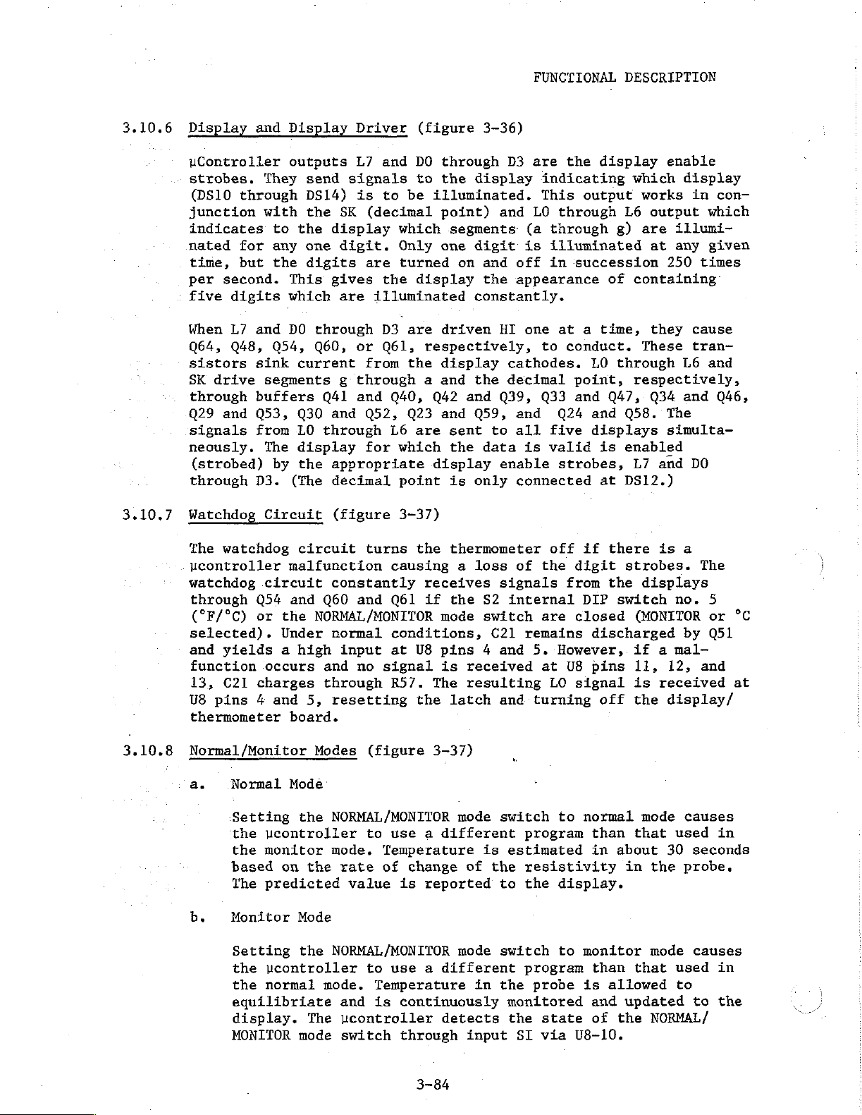
3.10.6
3.10.7
Display
and
uController
strobes,
(DS10
through
junction
indicates
nated
time,
per
five
When
064,
sistors
SK
through
029
signals
for
but
second.
digits
L7
048,
drive
and
and
sink
buffers
053,
from
neously.
(strobed)
through
Watchdog
D3.
Display
outputs
They send
DS14)
with
to
any
the
This
the
the
one
digits
which
DO
through
054, 060,
current
segments
Q41
030
LO
through
The
display
by
the
(The
Circuit
Driver
L7
and
signals
is
to
SK
(decimal
display
digit.
gives
are
which
Only
are
turned
the
illuminated
D3
or
Q61,
from
g
through
and
040,
and
052,
L6
for
which
appropriate
decimal
(figure
point
3-37)
(figure
DO
through
to
the
display
be
illuminated.
point)
segments
one
digit
on
display
constantly.
are
driven
respectively,
the
display
a
and
the
042
and Q39,
023
and 059, and
are
sent
the
display
is
only
3-36)
D3
and
(a
is
and off
the
appearance
HI
one
cathodes.
decimal
to
all
data
is
enable
connected
are
the
indicating
This
LO
through
through
illuminated
in
succession
at a time,
to
conduct.
point,
033
and 047,
024
five
valid
strobes,
display
output
L6
g)
of
LO
through
and 058.
displays
is
enabled
at
DS12.)
enable
which display
works
are
containing
These
respectively,
output
illumi-
at
any
250
they
L6
034
and
The
in
con-
which
given
times
cause
tran-
and
046,
simulta-
L7
and
DO
3.10.8
The
watchdog
ucontroller
watchdog
through
(°F/°C)
selected).
and
function
13,
U8
pins 4 and
yields
C21
circuit
054
or
the
Under
a
‘occurs
charges
thermometer
Normal/Monitor
a.
Normal
Setting
the
ucontroller
the
monitor
δ.
based
The
Monitor
on
predicted
Setting
the
ucontroller
the
normal
equilibriate
display.
MONITOR
circuit
turns
malfunction
constantly
and 060 and
NORMAL
high
5,
/MONITOR
normal
input
and
no
through
resetting
board.
Modes
Mode
the
NORMAL/MONITOR
to
mode.
the
rate
value
Mode
the
NORMAL/MONITOR
to
mode.
and
The
ucontroller
mode
switch through
the
thermometer
causing a loss
receives
061
if
the
mode
conditions,
at
U8
pins 4 and
signal
R57.
(figure
the
is
The
latch
3-37)
mode
use a different
Temperature
of
change
is
reported
use a different
Temperature
is
continuously
detects
signals
S2
switch
C21
received
resulting
and
switch
is
of
the
to
mode
in
switch
the
input
off
of
the
internal
are
remains
5.
However,
at
LO
turning
to
program
estimated
resistivity
the
display.
to
program
probe
monitored
the
state
SI
via
if
digit
from
DIP
closed
discharged
U8
pins
signal
off
normal
than
in
monitor
than
is
and
of
U8-10,
there
strobes.
the
displays
switch
(MONITOR
if a mal-
11, 12,
is
the
mode
that
about
in
that
allowed
updated
the
isa
no.
by
received
display/
causes
used
30
seconds
the
probe.
mode
causes
used
to
to
NORMAL/
The
5
or
Q51
and
°C
at
in
in
the
3-84
FUNCTIONAL
RNIO
10K
8PL
DESCRIPTION
NOTE:
U1
cor
44461
/8 = 8
/5 = 5
SA
LINES
THRU
DA
THRU
LINES
SG.DP
DE
(SA-SG,DP)
(DA-DE)
s
RN4
&PL
10K
5
TO
| i
+
1
I
!
1
to
上
i
i
| i
|
I
1
RES
pe rr
Ly
—
PIO
P16
Pu
P20
P24
—
CIM
ost
TRU
trae
|
|
OPTION
ONLY
9
es
-B
の
<
<
o
8
В
me
L
5
©
1
1
|
i
1
1
1
I
I
|
i
Figure
3-36.
Temperature
Display
3-85
and
Display
Driver
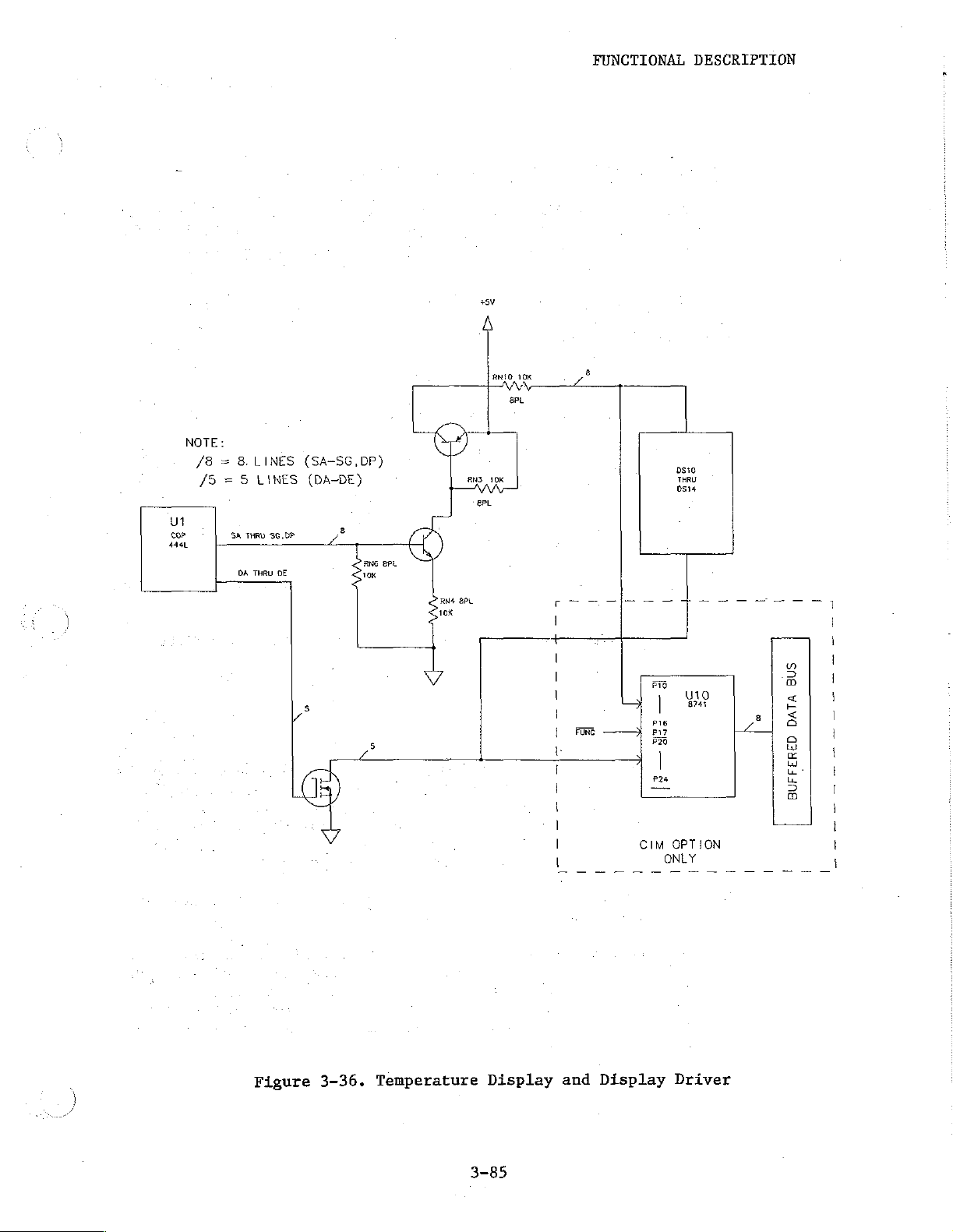
3.10.9
32
Internal
DIP
Switch
No. 5 (°F/°C)
FUNCTIONAL
(figure
DESCRIPTION
3-37)
3.10.10
Setting
causes
temperature.
through
The
holes
S2
in
the
the
input
internal
position;
Power
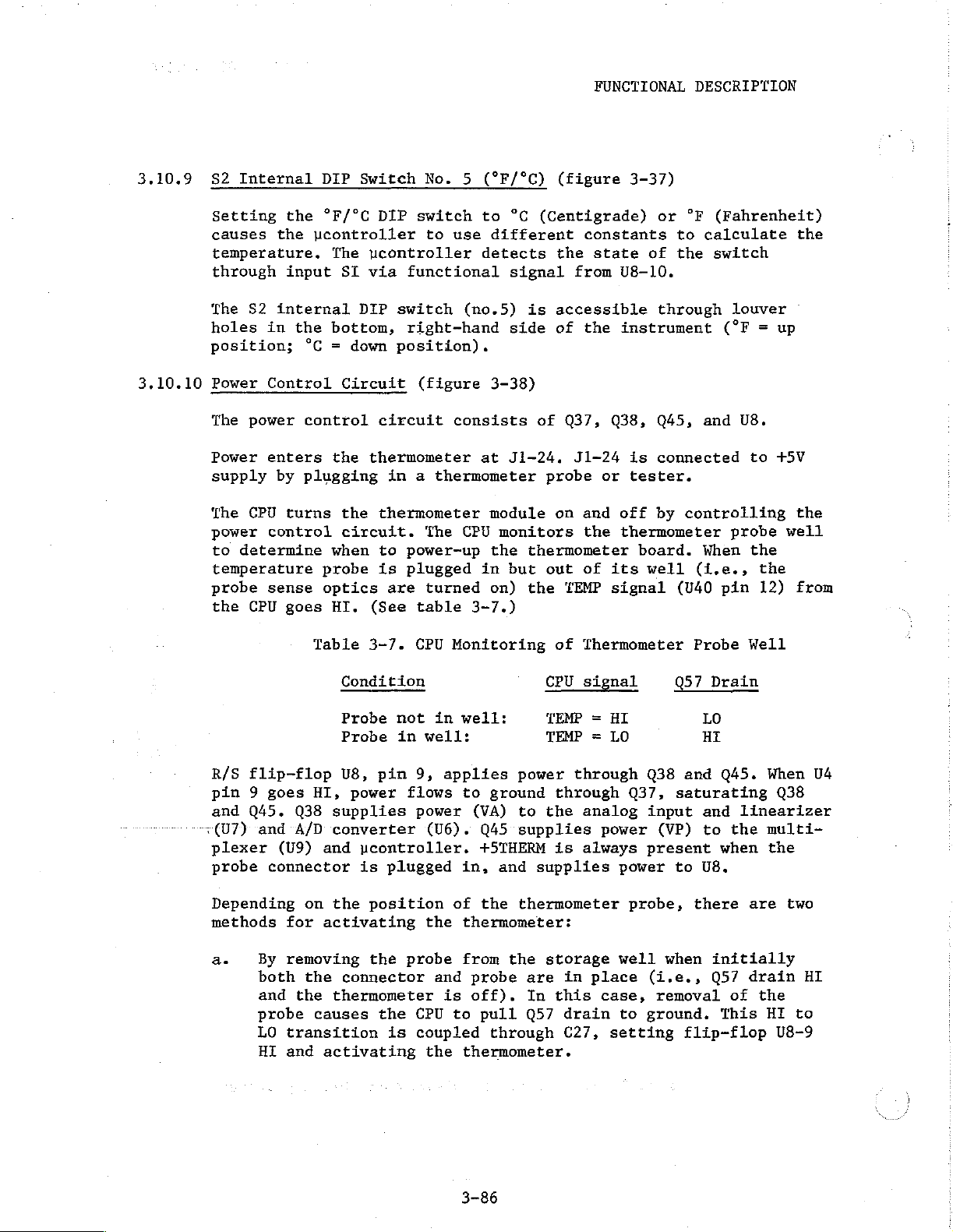
The
Power
supply
The
power
to
Control
power
enters
by
CPU
turns
control
determine
temperature
probe
the
CPU
sense
goes
°F/°C
ucontroller
The
SI
the
bottom,
°C = down
Circuit
control
the
plugging
the
circuit.
when
probe
optics
HI.
Table
DIP
switch
to
use
ycontroller
via
functional
DIP
switch
right-hand
position).
(figure
circuit
consists
thermometer
in a thermometer
thermometer
The
to
power-up
is
plugged
are
turned
(See
table
3-7.
CPU
Monitoring
to
different
detects
(no.5)
3-38)
at
module
CPU
monitors
the
in
on)
3-7.)
°C
(Centigrade)
the
signal
is
accessible
side
of
of
J1-24,
probe
on
thermometer
but
out
the
of
constants
state
from
U8-10.
the
instrument
Q37,
Q38,
J1-24
or
and
off
the
thermometer
of
its
TEMP
signal
Thermometer
or
to
of
the
through
Q45, and
is
connected
tester.
by
board.
well
(U40
°F
(Fahrenheit)
calculate
switch
louver
(°F = up
U8.
to
controlling
probe
When
(i.e.,
Probe
pin
the
the
12)
Well
the
+5V
the
well
from
R/S
flip-flop
pin 9 goes
and
Q45.
v(U7)Y
and
plexer
probe
connector
Depending
methods
8.
By
both
and
probe
LO
HI
Condition
Probe
Probe
U8,
HI,
Q38
supplies
A/D
converter
(U9)
and
on
the
for
activating
removing
the
connector
the
thermometer
causes
transition
and
activating
not
in
well:
pin
9,
power
flows
power
(U6).
ucontroller.
is
plugged
position
the
the
probe
the
CPU
is
coupled
the
in
well:
applies
to
ground
(VA)
Q45
+5THERM
in,
of
the
thermometer:
from
and
probe
is
off).
to
pull
through
thermometer.
CPU
signal
TEMP = HI
TEMP = LO HI
power
to
supplies
and
through
through
the
analog
is
always
supplies
power
power
thermometer
the
storage
are
In
Q57
in
this
drain
C27,
well when
place
case,
to
setting
Q38 and
037,
input
(VP)
present
probe,
(i.e.,
removal
ground.
Q57
Drain
LO
Q45.
saturating
and
to
the
when
to
U8,
there
initially
Q57
of
This
flip-flop
When
038
linearizer
multi-
the
are
two
drain
the
HI
to
U8-9
U4
HI
3-86
NOTTdTMOSd
'IYNOLLONNA
SAVIdSIO
OL
€
qsta
SAVTdSIG
OL
0910
SAVÍdSIG
OL
ala
907YNY/91907
VOL
00008
NON
|
-
GrIPNL|
so
Y
GrLANL]
rm
Y
GPISNL
oso
y
e
[la
|
-ná
|
0/d
|
er
„я
=
2
AMO11931SS
‘UOLINON/IVAZON
HOITAS
gs
o
4
|
1
-ions
ии
|
33
oc
|
ος
AON
|
A
wot
AAA
o/a
ir
088
M0014
て
eg
İsi
1071
Vos
SATNOITI
10399198
ii
9/4,
рив
‘лозтиок/тешлом
{8-Е
‘ЗорЧэзем
ver
Sn
Od
do
1s
420+
sn
7
πι
HOt
NSC
sto
1
χοοξ
seu
458
nu
M
y
éco
vazzena
AOS/E
a;
"€
aso
eu
VELICNA
YS
て
Nd
098
Ms
91
so”
>
UT
x=
e
0/4
©%
cn
090
Try
900
190
за
τε
19
*/5-$
da
эла8тя
더
RgHH1
AS+
je
es
“버기
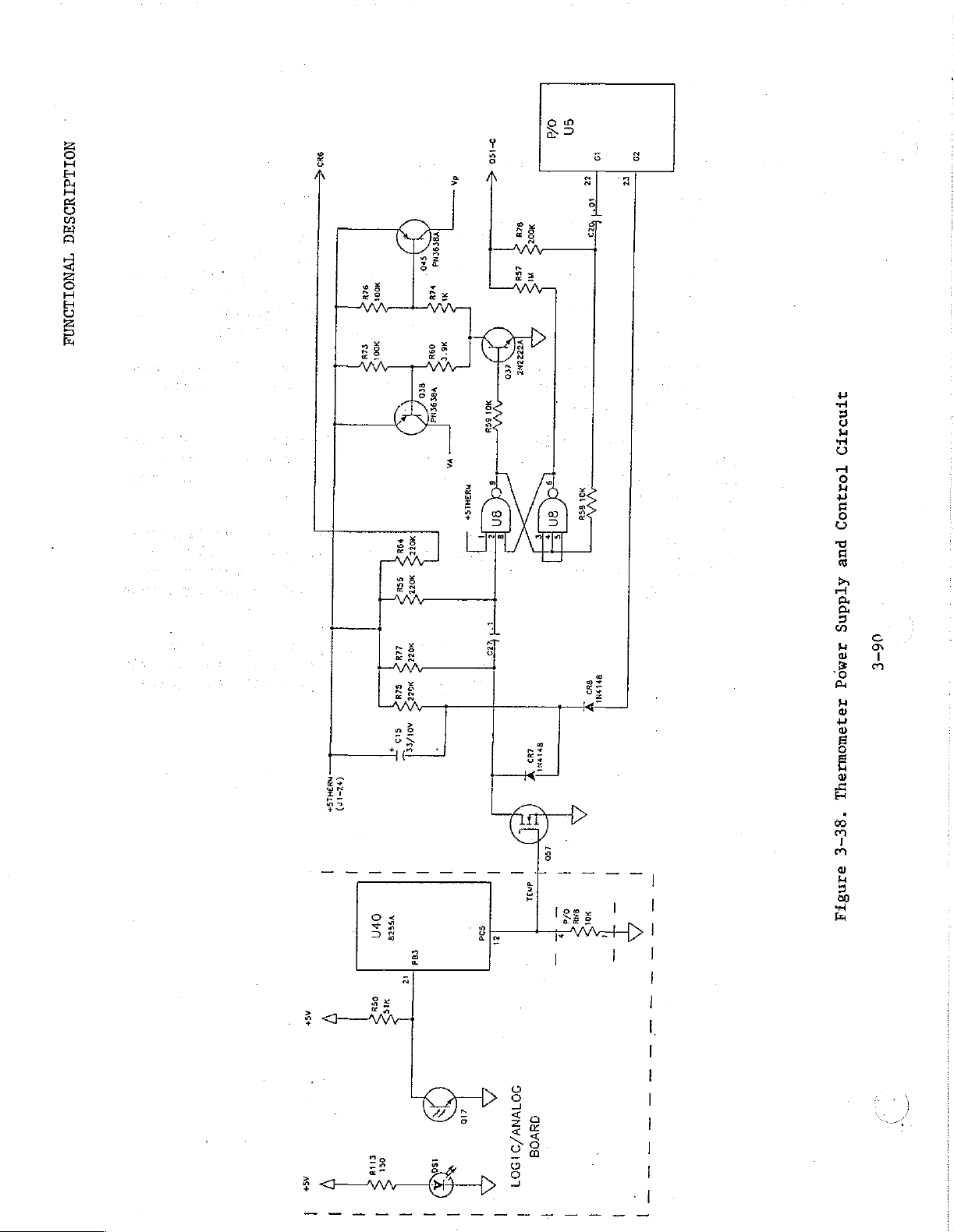
FUNCTIONAL
DESCRIPTION
3.11
b.
By
inserting
is
empty
through
level.
thermometer.
Application
power
through
ization
The
is
first
R14
to
occur.
thermometer
Alternatively,
causes
U8-9
condition
CIM
The
blocks.
instrument
The
the
to
flip
EQUIPPED
CIM
equipped
These
blocks
ucontroller
through
through
are
thermometer
(i.e.,
R56,
This
delay
of
power
applied,
delays
can
inserting
to
LO.
MODEL
Model
blocks
an
display
the
probe
Q57
and
U8
causes
from
the
rise
be
deactivated
to
The
CR7 and
4200C
4200C
are
an
RS-232
IVAC
CIM
interface
connector
drain
pin 2 is
LO).
U8
045
initializes
VP
goes
HI
of
RST
the
probe
output a LO
ucontroller
CR8
via
contains
designed
port.
II
board, a real-time
port.
when
In
this
held
LO
pin 9 to
and
RST
to
logical
by
removing
into
the
to U8
senses
its
G2
three
to
permit
the
case,
until
become
the
ucontroller.
is
LO,
1,
probe
pins 4 and
the
port.
additional
ASCII
probe
storage
+5V
C27
charges
HI,
activating
Charging
allowing
the
probe
storage
inserted
monitoring
clock,
well
charges
to a HI
When
C8
initial-
connector.
well
5,
causing
probe
functional
of
and
a
027
the
the
3.11.1
CIM
Interface
The
CIM
equipped
which
verters
II
cated
carries
Ul6
loading
access),
a
when
The
upper
an
The
from
operation
The
It's
WR-
contains
to
board
HI
IO
is
connector
only
is a bi-directional
from
and the
to
avoid
Ul6
is
address
eight
transfer.)
read
CIM
or
the
board
timing
RD-.
or
Sl
and
(figure
Model
a
UART,
interface
interfaced
is
the
signals
the
data
data
ambiguous
not
enabled.
lines
address
write
status
HI
is a read
is
selected
is
derived
3-39)
4200C
baud
to
to
in
parallel
bus.
direction
IOA0
and
lines
command
line
from
an
external
the
and
buffer
It
logic
ΤΟΑΙ
copy
to
from
operation.
for
incorporates
rate
generator,
4200C
with
power
is
levels
the
the
an
the
used
enabled
is
are
the
CIM
CPU
I/O
address
required
determined
lower
an
data
gathering
through
the
test
to
isolate
by
on
the
buffered
eight
board
as
IOWR-.
operation
decoder
IVAC
and
J4.
connector
by
the
the
EXTIO-
by
external
ADDR8
address
is
derived
LO
when
CIM
II
RS232
This
system.
16-pin
CIM
CIM
(external
RD-,
bus
and
level
RN2
and
is a write
IOXSEL-
output
board
J5,
II
board.
board
maintains
IODQ-I0D7
ADDR9.
lines
buffered
EXTIO-
con-
The
dedi-
but
I/O
during
is
CIM
(The
LO.
and
+5
Volts
and +12
volts
are
provided
3-88
at
J4
to
operate
the
CIM
board.
FUNCTIONAL
DESCRIPTION
3.11.2
Thermometer
The
thermometer
the
display/thermometer
and
64
bytes
digit
are
code
interface
is
The
can
temperature
The
clock
reset
eter
U10
ture
P25 and
driver
processed
and
four-digit
is
not
compatible
thermometer
occur
with
thermometer
signal
(BRESET)
display
ports
P10-16
display
P26
NORMAL/MONITOR
1-6).
Display
interface
of
RAM.
signals
to
convert
required
with
interface
the
display.
display
(BCLK)
from
interface.
and
segment
monitor
switch
Interface
(U10)
board.
It
decodes
and
thermometer
the
BCD
code
because
the
CPU
interprets
thermometer,
interface
from
the CPU
the
P20-24
and
digit
is
serve
thermometer
and
the
Circuit
is
It
contains
temperature
display
for
transmittal
the
multiplexed
data
as
is
CPU
via
inverted
as
strobe
power
S2
internal
(figure
an
8741A
control
information
bus and
all
possible
well
as
clocked
Ul2,
pin 6 and
to
input ports
signals,
status
DIP
3-40)
satellite
1K
byte
display
signals.
to
to
the
temperature
CPU's
timing.
conditions
the
contents
by
the
initialize
for
respectively.
and P17
switch
`
processor
of
program
segment
These
an
8-bit
CPU.
ROM
and
signals
status
The
display
that
of
the
buffered 3 MHz
4.
Power-on
the
thermom-
the
tempera~
TO,
monitors
settings
the
(nos.
on
Ull
functions
display
tently
kHz).
decimal
clocked
as a pulse
point
at
the
(BDP),
thermometer
stretcher
because
monitoring
the
decimal
ucontroller's
the
temperature
point
clock
is
rate
intermit-
(62.5
3-89
NOIL4I4DSAG
SUI
da
Iso
o/a
sn
25
to
cez
TVNOTIDNAA
seu
teu
MOOL
3001
Xk
seu
s3
+
seo
ye
osu
eso
verocnd
30202:
Aot/ce
Yecectd
wt
46°C
YA
Nd3H1S+
・
MOL
658
4
て
Tn4FO
1043909
MOL
864
SPL
sen
ONL
y
pur
ATddng
ὐό-ε
19Mog
1940mou19yj,
ASI
ASI
3HLS+
Ozer)
070
osu
CI
Ysszg
Nes
ost
tes
isd
£10
θε-ς
91N3TA
201VNV/91901
08708

NOILATVISIA
TYNOLLONAA
へ
AS+
M9
ENH
V
Li
CU
Lo
=
УГ
ee
0001
[001
EFE
İSİ
İİ
LT
aT
Igo
30
le
č
an
σον
ET
2001
St
970
у
20/\
gi
3
EĞİ
rodi
ET
ST
S
S
say
vů/y
5;
or
a
(2001
(5001
[door
zt
EF
TE
By
16
207
7
8
90/y
90/
VI
F
é
i
[=
wo:
£
95205.
NO
NI
Fer
60007
8
2
一
9/N
一
Fi
100
NI
0cn
ino
0/d
NI
ee
GT
y
en
0
ARM
AGH
ye9HPZ
一
6
-136X01
00gHpz
9
009HyZ
a
5
ya
E
00392
ээеулезит
ито
T6-£
‘65-6
эло8ря
еп
ャ
be
0/d
た
—
eL
Ano
NT
"NE
ー
A
EE]
PO
ντ
[τση
TESA
TE
κου
TTO
ο
.
GIN
pyg9HbZ
0/а

NOIL4I89SAG
"ITVNOTIINNA
-9-858
一
一
1
|
1
!
NOILdO
er
3-070
9-9rp
290
9-6e0
一
一
一
一
十
|
|
1
!
1
1
1
1
!
|
一
ter
ID
9-50
Seo
'si-sn
一
A
DT
0000
0-760
0-089
a
CT
—
——+
—
Ena
86
0-598
Τρ
|
| |
ㅣ
1
|
I
|
I
!
ne
POSHPL
y
E
ci
n
LE
LL
2
POSHbZ
오
g
Soo
121
|
5
n
aos
A+
ORE]
NE
#159
788
1
1
|
I
ANO
WII
NF
cod
!
I
i
т
FOO"!
0663
a-
|
!
xo
ou
ASH
AS+
dA
9
8
sin
te
i
一
ax
È
M
ss
=
ix}
e
5
AB
本”
'
eso
154
-L
s
|
DE
5
VSB
DE
858
-751
GE)
82]
2)
9044
pg
lid
©
.
ou
try
[SE
98
σε
σα
u
358
Rose)
re}
219
Sid
4882
BAKI,
EE
ds
=
о
=
απο
Ее
tê)
Old
уч
Ov
3
ove
=
-0610
zorla
dal
851
ge]
tel
009
28
eg
/Běd
so
50
La
Par
67
Siva
01008
PİR
1
|
are
si-ip
2
TEST
ーー
=
~8g]
E
W
640/929
XY0/zed
ms
to
Ed
EO
va
[et
ET
で
3
[pr
VIVE
20108
Eyly06
Tuivog
|
Te
L
è
ČB-
€
©
9-1
PIC
pin
-
M
AN
a
AĞI
00
ㅣ
に
TH
+=
12
>
ээвулезит
Аетазта
лэзэшошлечл
66-5
‘07-6
элоЗтя
|
|
1

FUNCTIONAL
DESCRIPTION
3.11.3
Real~Time
The
real-time
the
CIM
ments
tor
is
+5VAO
the
clock
Clock
equipped
to
external
the
(+5
volts
continues
time
(CIM
clock,
instrument
devices,
base
always-on)
Option
U29
(Y2).
to
is a power-off detection
(CS)
of
U29
time-keeping
PWRON
before
U28D.
from
the
The
pin 4 LO,
from
the
address
keeping
U29
flip-flop
disconnect
instrument
determined
through
to
HI,
uses
and
R14
to
applied
go
LO,
turning
the
data
and
set
R53
multiplexed
from
C33
an
to
from
the
+5
inverted
turning
disconnected
from
process
is
period
until
resetting
on
delays
internal
the
the
and
RAM
power
volt
decoder
setting
turned
05,
the
instrument
address decoder
data
regulator
logic
PWRON
off
until
on,
at
033 pin
U33
RS
connecting
feature
processor,
the
power
only,
on
the
logic/analog
for
providing
such
as
U29,
Y2,
from
the
function
with
circuit
during
board
Q5
supply
sets
which
U5-9.
from
is
R/S
disconnects
CS is
the
during a time
U29
is
not
the
CPU
1.
While
pin 2 is
HI,
flip-flop
U29
of
the
using
initial
fail
application.of
software
for
the
figure
printers.
and
also
power
the
which
disconnects
to
prevent
instrument
goes
removed.
flip-flop
then
bus.
U33-11
when
being
reset
(RESET)
RESET
delaying
U33-4
to
the
and
the
data
ALE
flag
first
time.
3-41)
board,
time
and
A
32.768
U33 are
regulator
instrument
disruption
power
LO
at
power-down
This
U33-4
the
active
pulled
prevents
CS is
LO,
accessed.
goes
is
HI,
reset
U33-10.
address
bus
to
derive
control
+5VAO
in
U29
is
included
date
kHz
powered
board
turned
the
chip-enable
of
measure-
oscilla-
so
off.
of
down. A signal
time
is
inverted
and
U33-10
low
CS of
HI
through
R52,
the R/S
delaying
When
high
C56
and
the
for a pre-
charges
causing
Pin 4 then
decoder
line.
when
to
U5-9.
both
Network
U29
power
address
pin
by
that
the
by
with
the
pin
goes
U29
22
is
in
the
U33
U29
3
U33-4
also
provides
the
power
status
signal
PWR_GOOD
to
U31
and
032.
3.12
3.12.1
e
SOFTWARE
This
the
instrument
thermometer
mometer
the
COP444L
in
one
32
Thermometer
The
thermometer
performs
the
S2
internal
mode
removing
the
front
tion
the
thermometer
switch,
and
program
ucontroller.
KB x 8
Program
tasks
and
the
probe
of
the
features
contains
and one
resides
EPROM
program
based
DIP
on
on
switch
the
from
instrument).
is
integrated
(see
section
two
entirely
for
the
blood
in 2 KB x 8
The
blood
and
is
executed
separate
pressure
of
ROM
pressure
by an
is a noninterrupt-driven
the
settings
no. 5 (°F/°C),
internal
or
replacing
A
description
with
probe
of
the
and
detéct optics
it
into
the
electronics
3.10).
programs,
monitor.
which
is
located
monitor program
80C85
CPU.
program
DISPLAY
the
the
of
TEST
NORMAL/MONITOR
(activated
storage
the
program
description
one for
The
ther-
inside
resides
that
switch,
well
opera-
by
on
of
3-93

NOILATHISAG
RR
|
TYNOLLONDA
OVAS+
—
|
m)
ZA
zHy894
100100
τς
8
3
|
ss3uadv
4300930
AYOWSN
sn
6
135914
VZZTZN
{D
if
|
一
MOL”
vig
,
q
vv
10
一
2753
2x
FE
SAM
1X
Ez
|
l
SE
一
|
|
|
aree
Sgr
un
SE
DE
ee
pe
to:
+
ee]
A
LMONTO
sv
E
|
9000]
25%
|
ET
nos
AN!
sors
so
들뜨게
0
E
|
A
я
9
1.
0007
|
Y
|
S
т
194
|
|
seep
оо
19
+
t
|
000
NOtidO
ANO
WID
68199
g
181
수
|
0009
MOL
64
e
E—
-
|
1
一
一
一
一
一
一
一
一
一
一
一
sou
xo
Ἠ9οτο
SUFI-TUSY
767€
*Ty-E
owns
AL
ose
74
ast
sua
01
:
es
°
LNi91y
AS+
и
D
|
61041
82N
wor:
BERNE
$60709
Or
FeorQo
T
12538
BINBTA
Aos/z
VAN

FUNCTIONAL
DESCRIPTION
3.12.2
Blood
The
are
Pressure
blood
linked
another
perform
a.
Cuff
b.
Deflate
c.
Compute
d.
Calibrate
e.
Offline
г.
5.
Figures
Diagnostic
Redisplay
program
3-44)
are
the
about
interrupt.
pressure
together
module
the
inflation
3-42
flow
show
how
START/RESET
every
Program
monitor
perform
following
blood
display
pressure
tests
values
through
is
shown
the
683
microseconds.
at
tasks:
or
test
(memory
3-44
in
two
switch
program
load
time.
interrupt
pump-up
mode)
depict
figure
interrupts
and
The
is
Three
processing
program
3-42,
are
the
time
real-time
organized
modules
tasks.
operation.
Flowcharts
processed.
base
interrupt,
clock
=
into
modules
and a segment
The
remainder
The
main
(figures
The
two
occurring
3-43
interrupts
is a third
that
of
and
When
power
failsafe
this
time,
completing
and
other
exits
auto-start
occurs.
motor
longer
hardware
the
While
is
off and
than
is
the
the
data
wait
condition
display a FIX
switches
to
When a blood
enters
and
blood
the
inflate
data-taking
pressure
first
are
program
diagnostics,
values
loop
in
the
that
20
seconds,
ME
message.
see
if
pressure
cycle
and
applied,
executed.
will
and
to
start
is
detected
wait
the
If
the
calibrate
measurement
cycle.
is
returns
software
diagnostics
If a malfunction
display a FIX
the
finally
a
loop,
cuff
either
Also
When
program
enters a wait
blood
or
the.
pressure
test
during
mode
has
inflation
initializes
pressure
when
program
does
fails,
wait,
has
been
entered. Finally,
to
the
wait
loop.
ME
message
measurement
the
START/RESET
checks
not
the
it
been
requested,
is
complete,
the
of
memory
is
detected
and
various
loop.
that
exceed
instrument
tests
the
selected.
program
halt.
The
program
when
interrupt
the
20
mmHg
internal
the
program
the
deflate
computes
and
at
Upon
timers
the
pump
for
will
the
3-95

The
START/RESET
function
program
Instead,
shown.
for
example,
(or
monitors)
the
interrupt.
The
each
organized
example,
the
does
it
The
time-base
time
the
so
the
milliseconds.
returns
tion
instrument
when
to
is
detected.
the
diagnostics
interrupt
operator
not
return
passes
control
START/RESET
during
the
state
interrupt
interrupt
that
microphone
the
each
When
execution
interrupted
The
offline
display
has
control
interrupt
memory
of
program
occurs
branch
signal
time
are
program
requested
to
the
mode.
the
START/RESET
(see
is
is
of a branch
program
base
test
performed.
FUNCTIONAL
(figure
to
the
main
can
In
and
be
memory
3-43)
responds
interrupted
program
disabled;
mode,
switch
executes
executed
sampled
figure
one
3-44).
periodically.
and
is
completed,
unless a failsafe
interrupt
is
being
is
executed,
determines
accordingly.
location,
at
the
it is
the
instead
of
several
The
processed
disabled
and
DESCRIPTION
what
location
disabled,
program
of
branches
program
For
every
control
error
when
at
condi-
the
power-on
The
polls
using
'
is
two
3.12.3
Hardware
the
Checks
computer
conditions,
condition
displays
fying
meanings
the
is
a
type
appear
displaying
power
through
only
and L to N are
Tests
-
ing the
value.
tions
expected
listed
on
switch
K
once each
corresponding
value
The
for
input
in
the
failsafe
(also
tests
table
program
initially
detected,
FIX
ME x message
of
in
the
message
on
and off.
W,
time
performed
of
failsafe
corresponding
code
5-1,
input
tests
problem
chapter
at
power-on
the
and
Tests
the
instrument
(where
found).
5.0.
can
X, Y and Z for
power
to
the
output
and
Table
is
periodically.
messages
failsafe
port,
the
5-2
and
output
output
instrument's
and
x
The
The
only
for
FIX
CIM
applied;
A
through
input
FAILO,
to
messages
code
summarizes
ports.
hardware
periodically.
beeps
is a number
values
computer
be
ME
audibly
restarted
conditions
equipped
tests
port,
N
FAILI,
is
D
for
are
used
through
(where
the
If
five
or
letter
for x and
program
by
cycling
instruments)
conditions
executed
with
to
simulate
K.
appropriate)
meanings
for
unsafe
such
a
times
identi-
their
halts after
the
0,
2,
and
are
4,
5,
by
compar-
an
expected
condi-
Both
the
are
of
the
bits
and
|
i ;
i
A
run
3-96

FUNCTIONAL
DESCRIPTION
When
must
value
Example:
the
match
is
masked
displays
outputs
comparison
by
the
to
of
the
Pulse
FSDIS
Binary
Octal
Then
signal.
is a problem
The
"nm,
compare
The
motor
was
the
expected
the
FIX
the
PULSE
failsafe
dispiay
/
test
software).
ME
message
FSDUMP
is
input
display,
input
041
©
made,
code
If
for
in
port.
with
FSMOT
0 1 ο
0 4
with
good
with
tables
signal
the
detectd
5-1
corresponds
motor
as
or
being
and
motor
failsafe
they
the
octal
FIX
5-2
on
when
(failsafe
do
not
particular
representation,
ME
D.
FSCOMP
9
to
determine
to a 061
detect
the
input
bits 0 through
bit 7 is
match,
test
/
FS2
ο ο 1
code.
circuitry
motor
should
not
the
program
being
the
FS1
1
the
faulty
Therefore,
in
be
used
run
actual
FSO
this
off
6
and
and
there
case.
(a
3-97

POWER
DIAGNOSTICS
|
INITIALIZE
T
MOTOR
CUFF
TESTS
BRATION
MODE
SELECTED
ON
t
AND
PRESSURE
CALI
NO
FUNCTIONAL
DO
CALIBRATE
FUNCTION
DESCRIPTION
AUTO
START
INFLATE
DEFLATE
AND
DATA
COMPUTE
BLOOD
AND
YES
COLLECT
|
PRESSURE
PULSE
NO
Figure
3-42.
Main
3-98
Program Flowchart

START/RESET
INTERRUPT
FUNCTIONAL
DESCRIPTION
i ;
Figure 3 -
]
MEMORY
Y
NO
DO
OFF
LINE
YE
DISPLAY
DO
MODE
TEST
MEMORY
FUNCTION
42
Figure 3 -
Figure 3 -
;
42
42
NO
Figure
3-43.
START/RESET
3-99
Interrupts

TIME
.
GO
TO
TIME
Go
+
SAMPLE
RELATIVE
PRESSURE
SLOT
OOLEACH 8 MSEC)
+
PROCESS
RELATIVE
PRESSURE
SIGNAL
RETURN
…
O4{EACH
SLOT
To
16
DEFLATE
MSEC}
TIME
BASE
INTERRUPT
1
ATIEACH 2 MSEC)}EXZIEACH
REL
PRES
(
2
MSECRX3(EACH
DISPLAY
SAMPLE
ABSOLUTE
(ERRE
AND
UPD
DISPLAYS
Г
RETURN
)
3
O8(EACH 8 MSEC}
TIMERS
|
UPDATE
SOFTWARE
TIMERS
Y
{
RETURN
TEIEACH
} (
FUNCTIONAL
2
MSEC}
MIC
6S
MSEC) | TEST
+
SAMPLE
PROCESS
PHONE
RETURN
OTHEA
DISPLAY
SWITCH
SAMPLE
DISPLAY
PUSH
TEST
BUTTON
:
y
RETURN
DESCRIPTION
AND
MICRO-
SIGNAL
)
UPDATE
RETURN
Y
D/A
Figure
3-44.
Time
Base
3-100
BATTERY
DEAD
Oe
MESSAGE MESSAGE 4 SHUT
HALT
PROGRAM
Interrupts
DISPLAY
CHARGE
INSTRUMENT
%
HALT
PROGRAM
BATTERY
OFF
RETURN
-
\

1.0
INTRODUCTION
This
chapter
detailed
4200.
Chapter
For
Three,
contains
system
specific
CHAPTER
the
operation
schematic
FUNCTIONAL
FOUR ~ SCHEMATICS
schematic
of
the
diagrams
VITALeCHECK
partial/block
DESCRIPTION,
of
that
instrument
diagrams,
this
manual.
depict
refer
the
-
Model
to
NOTE:
issue
board
Schematics
of
the
printed
revisions.
included
circuit
in
this
manual
boards,
and
represent
may
not
the
reflect
original
future


SDILVNI
8300930
553400
5ー
prgog
タ
(9
/Zー
30
タ
8orenw/
1
30049)
っ
FSo7
・Tー
タ
9rn8T
πα
pres
η
INOTLdO
I
HIS
3118
H01VH3N39
110
|
+
HBOTAIO
0019.


SILLY
pısog
9/
(9
タ
ー
30
タ
8oTeuY/5Y3oT
7
29948)
"Try
axn3Td
자 99675
vo
ON
482/04
>
PEUR
bo
,
CE
ze)
ly
mp
“ir
ESD]


рлеоя
2-9-9
(9
30
Зотеиу/эт8от
Е
39248)
*1-$
элита
더
versare


SOLLY,
parog
6-7/8-9
(9
30
Βοτεαγ/οΓ8οΊ
4
39948)
"1-5
θαπ8τά
ET
一
1


SOIL!
B
[EOS
ASEM
PS
ALAN
PAF
Is
SO
RT
SAN
SUMO
santa
SEZAR
dplstS3
SELON
OE
T_T
CENERE
이이
Lelis!
es
Та
[ва
ва
ив
ons
4
sa
Niwt
SONO
4
une
A
mubasa
AN
a
SNA
ный
YOLLAYAN
4
€
“E
#29:
Ly
Ly
[Ik
LT
5
529G
YaAoloso
Si-yiE9
[Г
Yf-682|
ogfu-eet
I
cora
000
839.
gin
VID.
TEO
197
sn
em:
E
om
53;
m
ob
Los
To
a
le
Let
η
ven
4
E.
i
©
но
al
=|
8
des)
T
,
一
一
вание
e
Те
+
gl
8
號
29:
т
[ες
s|
3
06906
τις
εἰ
5
a
τη
2
8
482/06]
Sr
+
4ce/0r]
Müz
—1
>
sal
ua.
yl
ΡΕ
Jong
と
я
097
|e]
E
|
Te
i
[ome
8η
+ 3 +
]s
|
200:
다
|
99
810
Tos
o
à]
|
vats
an
oF
|
al
一
Lig
=
e
fa
İran
ral
G
С
a
o
Sa
Ч
a
B-
gl
9
5
一
q
q!
3
mr
τι
|
BEN
q!
B-
5
s.
5
,
conte
OL
a!
TU
5
sro
rl
|
ae
(ЕЙ
nil
ое
хе
402/01
BZ
Er
[
e
peri
Tal
LE
ont
|
gen
a
|
ast
|
etape
Gen
|"
|
roe
|
an
er
A
©
q
5
3.
w
q
5
に
5
sa
al
ses
5
mx
|
zen
KH
]
L
DÉS
|
nere
a
(그
£
品
m
T
T
F:
i
7
Е
8293
y
ῄ
|
:
ή
fp
g
g
É
É
È
5
55
gö
|
38
5
1192
800
1
PI
uo
‚||
T
προς
2
,
s
vessevo
era
r
ES
+
era
900
200:
090
ren
20:
:
e?
Sê
Nasem
©
i
3
Lİ
1
Sr
A
A
Г
o
tras
JadS+
À
+
astio
全
ms
À
+
E
『
|
>
u
С
와
一
900.
a,
TEN
|
ss
ven
|
ved
一
品
8
S
원
s
a
ve.
meer
TEN
|
|
es
|
|
gm
gen
ceb
çi
een
an
|
a
sl
mew
yl
|
oo
|
다
|
mw
el
ο
£T-9/T
pisog
(9
30
1-4
BoTeuy/oT807
9
39948)
"1-4
94N8T4
u
sr
2
a a
9
=
4


PTgog
S1=9/41-4
SOLAR
|
3
È
πο
ση
067
στη
αθηοποπαση1/«ετάθτα
(>
jo
T
19948)
"7-4
91N8TA
vaio
(elemeli


80120,
АУ
4510
97015919.
[IS
ET
asia
$ 1 1 ! i
"
.026
10017
71039
1
1
PTPO
41=0791-7
Xojamonisur/AeTdsta
(y
30
2
30046)
2-5
60874
43910
14918
11910
1437


pzeog
61-9/81-7
зазэшошлеци/АеТЯзта
(p
30
£
19948)
*2-у
элозта


Preog
129/0739
SDILYK
13
| .
141
SA
97
1
|
91690
|
001
ΕΕΤΤ
[
[veu
[es
[onu
|
60
|
[eo
em
“AS
"LIV
PÉORMONOIN
:IQardfOds
¥/1
SYMONE
A
a
SEMEN
Guy
SSA
вилл
SEZA)
SOLID
WOISISBO
Sato
-τ
“2
ET
ENDE
IT
Tree
“SISHOOS
37700
NE
KOT
RE
SRY
SAYWSIO
THY
7
A A
A
9160
geen
|
a
9680
pos
[
|
<:
2666
γη
品
s.
neon
5
se
n
52/0
ar
타
e
.498/0
as
타
ο
490/011.698/0(
ον
η
o
“
ts
Te:
+
[Ta
NA
y y
+
я
5
|
5
|
Tr
5
可
可
я
a
a
Lies
en
[sb
fd
[uso
sn
|
|a
다
|
ме
sh
feat
|]
|
[мы
BEA
[est
|||
|
Fin
в
|
feeb
ge
|
OM
|
à
L
|
또미
en
|a
x)
|
sono
en
=
È
。
。
[
$.
。
a
,
г
waren
va
sauves
40
je
lær
|
‘on
"
er
E
oe
|
ph
|
axe
root
cn
ong,
+
+
L
т
muro
Ware
바에
A
στη
1979W0119y1,/&eTdsTd
(7
30
4
29915)
-7-4
Sandra


SOLLVWAHOS
0350
0011407630
04008
ame
an
ame
ams
παπα
ere
daná
TART
en-s
00088
36NSS34d, U3AO
NA
DRE
ea
TT
MV
sor
TST
sme
sua
<
93437
εσ-η/εζ-ῃ
pavog
потаречелр
отзешпена
+6-ь
эдо8та
300383434
1634914
和
tar
e . 2
sr
ver
8-0
tin
в
©
he
8484
[o
mr
ο
M
m


2ー
PIPOg
タ
ター
SOLI
å
a
5
TORT
Tora]
a
a
1997
|
—
ET
vi
182945)
um
“Sais
br
00"
Adi
ogi
SST
Ες
ο
PUB
ης
κ
aco
La
la
,
gez
GERE
"|
ros
ozssu
«>
borne
τα
VA
:
LT
LAS
ή
AT,
Ť
[
Ga
-
zl
=
667
二
OWAG+I
ade
.
E
Oia
|
po
oi
:
EOS
L
dm
μις
:
ERLENZI
Eno
Es
>
mle
ral
・
ㆍ
PŘES
e
SZ
(dno
sain
ún
・
.
Ť
1
ーー
oo
7
TT
ET
">
πο
SB
15
où
gb
kk
gro
veborao
PE
<
Yebopoo
ofa
Bu
(7
10JBTNBBY
Fo
1
39948)
IBMOS
*
タ
ー
サ
эла8тТа
タ
ovas
1190
EN
oa
te
YN
obory)
500
AN
ь
FLE
«ЗОВ
LLENA
«φανωφαούοιν
LA
OSHO
ISIMYBHLO
Ni
WI
auy
DAY
SannwvA
SEMINA
SS
ZINA
VOLIDYSVD
ora
:
SALON
2
CAI
ZN
NO.
=
ov
ase
WLObZNd
/
ST


と
マー
PIPOg
タ
/
9
SDILYK
|
*
ar
Shares
SR
sl
ÉTÉ
ων
ese
Bh
z
Go
pey
+
1
z
_
eum
Yogi,
るー
(Z
103PTn80Y
jo
7
19848)
13M04
*y—y
02
ㅁ
97
EOI
voor
suvo
D101
pa
ae
ο]
vez
Caria
sor
SY
|
ss
sir
È:
s
осени
I
|
og
LT
ως
[Tel
Fe
+
L
pan
co
o
ο
os
|
MIA
]
AGE
E
Corvo
|
-
CAM
Te
Sand
we
5+54
=
299
VTZTANG,
づ
Rg
T
озна
Lar
(a
|
29
M


CHAPTER
FIVE - TROUBLESHOOTING
5.0
INTRODUCTION
This
chapter
instrument
before
save
Should
a.
b.
CAUTION:
shooting
Logic
"HI"
The
a.
b.
attempting
time
a
problem
That
The
integrity
Always follow
this
levels
state,
following
Table
Table
provides
should
and
the
are
and
5-1.
5-2.
repair
to
service,
may
avoid
occur,
instrument
of
instrument.
defined
zero
volts
is
an
outline
FIX
ME
Failsafe
help
the
in
be
necessary.
unnecessary
first
is
being
cuff
static
as a nominal
for a "0,"
to
Alarms
1/0
troubleshooting
Referring
repair,
ensure:
or
repair.
operated
and
cable.
grounding
procedures
potential
"LO,"
the
tables
Ports
the
replace
properly.
or
iù
this
VITALeCHECK
to
this
any
when
of
+5V
logic
chapter:
chapter
component
trouble-
for a "1"
ground.
will
or
ο.
d.
e.
f.
5.
Table
Table
Table
Table
Table
5-3.
BP
System
5-4.
Thermometer
5-5.
Power
5-6.
Logic/Analog
5-7.
Display/Thermometer
Troubleshooting
System
Regulator
Board
Troubleshooting
Board
Voltage
Voltage
Board
Guide
Guide
Specifications
Specifications
Voltage
Specifications
5-1

TROUBLESHOOTING
HARDWARE
This
instrument
these
check
The
this
checks
that
use
section.
section
Tests
CIM
on.
operation,
FIX
writes
for
equipped
Tests
ME
circuit
FAILI
(U-18,
expected
the
information
display.
Table
expected,
Table
5-1
5~2
CHECKS
fail,
failed.
of
the
If a FIX
5.2.
FIX
ME x conditions
instruments)
for
3,
conditions
an
8-bit
response
BDO-7)
value
This
octal
summarizes
correct
shows
performs
the
FIX
ME x messages
4, 5,
A
to K are
word
is
to
is
read
and
not
display,
obtained,
value
the
binary
the
significance
self-diagnostic
CPU
issues
a
for
ME x message
0,
2,
are
run
once
and L to N are
tests
failsafe
back
is
compared
to
of
output
the
the
and
displays
corresponds
alarm
output
messages.
is
shown
of
hardware
FIX
ME x message,
checks.
where
If
any
x
-
troubleshooting
does
not
appear,
and A to K (also W to Z for
when
run
the
CPU
with
CPU
an
to
each
the
periodically
failsafe
port
FAILO
through
an
expected
issues
octal
the
For
in
bit
an
value
8-bit
the
octal
BDO-7
is
continue
instrument
circuit.
(U7,
failsafe
value.
alarm
in
input
failsafe
for
reference.
in
the
explained
is
during
The
FS0-5).
input
If
message
the
PULSE
from
tests,
message.
of
is
the
in
to
the
turned
CPU
The
port
the
to
FAILI.
the
5-2

TROUBLESHOOTING
FIX
Code
0
2
ME
Type
EPROM
memory.
of
RAM
write/read
Attempt
Pump
motor
Cuff
pressure
Initial
(pressure
valve
or
failsafe
failsafe
clear,
test
multiplexer
Test
CRC
check
to
execute
on
power-on
greater
closed,
disconnect
or
incorrect
Table
check
failed.
more
exceeded
state
than
or
pump
disconnect
channel
5-1.
failed.
from
nonexistent
than
320
not
20
motor
flipflop
flipflop
pressure
FIX
100
seconds.
mmHg.
correct
mmHg,
activated,
being
comparator
selected).
ME
Alarms
or
set,
dump
or
held
Expected
Binary
00
110
000
Result
Octal
060
Failure
or
Failure
pump
dump
motor
to
valve
to
Simulated
comparator
simulation
Failsafe
sense
20
(FAILO
Failsafe
clock
00
Failsafe
comparator
simulation
Failsafe
simulation
Port = 00
comparators
mmHg,
Port = 00
loss
001
000).
detect
not
detect
not
able
20
mmHg
failed
(FAILO
20
mmHg
less than
clock
335
4.5
loss;
simulation
mmHg
failed
(FAILO
minute
timed
011
010).
dump
valve
able
pump
to
to
motor
be
pressure
less
Port = 00
and
failed
000
pressure
greater
Port = 00
out
than
335
335
mmHg
010).
watchdog
(FAILO
timer
prematurely
closure
be
closed.
on
turned
sense
20
000
mmHg
pressure
greater
simulation
Port
sense
than
O11
high
or
on.
mmHg
001).
than
failed
=
335
011).
speed
(FAILO
mmHg
00
00
00
00
01
01
00
010
100
110
111
110
111
111
000
000
001
010
000
O11
010
020
040
061
072
160
173
072

TROUBLESHOOTING
Failsafe
simulation
.
required
Failsafe
lock
conclusion
(FAILO
Failsafe
to
be
testing
Pump
at
idle
Pressure exceeded
20
seconds
Failsafe
comparator
upon
1/0
interface
4.5
time
1/0
on
command
Port = 00
disconnect
reset
(FAILO
not
off
state.
pressure
cuff
failure
failed
of
at
failed
inflation.
(U10) and
minute
(FAILO
port
from
power-on
100
by
the
Port = 00
or
dump
idle
between
timer
to
time
Port = 00
failed
the
101).
flipflop
CPU
valve
20
mmHg
state.
sense
to
detect
52-6
the
the
high
out
within
to
write-
CPU
at
failsafe
failed
during
000
power-on
100).
not
more than
20
mmHg
pressure
probably
thermometer
CPU.
speed
011
010).
the
testing
open
open.
the
01
00
00
00
00
111
010
110
000
110
100
110
000
110 000
172
060
064
060
060
RAM
or
interface
Failure
(U10)
to
display
Failure
(U10)
to
display
ROM
failure
(U10).
of
the
properly
segments
of
the
properly
segments
in
the
thermometer
read
or
the
digits
thermometer
read
or
the
digit
thermometer
interface
temperature
strobes.
interface
temperature
strobes,

TROUBLESHOOTING
Failsafe
Bit
Mnemonic
Failsafe
Input
7
0
FSDIS
FSDUMP
FSMOT
FSCOMP
FS2~FS0
Output
Port
(FAILI):
6 /
FSDIS
0 = Failsafe
1 = Alarm
0 = Dumper
1 = Dumper
O =
1 = Pump
0 = Pressure
.
1 = Pressure
Port
Table
hardware
Pump
See
(FAILO):
5-2.
Failsafe
U18
1/0
5 4
FSDUMP © FSMOT | FSCOMP
OK
condition,
closed
open
on
off
output
less
greater
(changes
than
system
20
than
during
U7
Ports
3
disconnected
mmHg
20
mmHg
testing)
/ 2
FS2 FSI #50
by
failsafe
1
0
Bit
Mnemonic
7
.
0 0
FS5
FS4
0 0
0
1
1 1
FS2
#51,
FSO
FS1
0 0
0
1
1 1
6 /
1 = Disconnect
FS3-
=
1
0
=
=
=
1 = Reset
flipflop,
select inputs
FS0
=
1
0
=
=
=
5
FS5
failsafe
Clock
No
90
375
Both
Select
clock
Hz
clock
Hz
clocks
to
pressure
Selected
Actual
Simulated
Simulated
Simulated
4
FS4
clock
FSDIS
Cuff
cuff
less than
between
pressure
3
FS3-
from
software
(when
comparators
Pressure
pressire
20
20
of
under
(APS)
mmHg
and
more
/ 2
control
software
335
mmHg
than
FS2
335
1
-FS1
control)
mmHg
0
FSO
5-5

The
following
5-2.
The
CPU
Chapter
simulate
compares
with
system,
and
displays
an
example
exercises
Three,
conditions
the
value
expected
the
CPU
an
illustrates
the
failsafe circuits
section
of
3.8
for
the
value.
issues
an
octal value
and
testing
failsafe
If
the
alarm
in
use
3.12.3.
is
FAILO
input
expected
message
the
PULSE
of
the
on
The
port
value
to
display.
failsafe
start-up
output
(U7,
the
as
port used
FS0-5).
FAILI
is
information
(U18,
not
TROUBLESHOOTING
tables,
5-1
discussed
to
The
CPU
BDATAO-7)
read from
display,
and
in
the
5.2
During
simulate
R19,
through
reset
software
failsafe
(step
(173)
the
U27,
start-up
a
R23,
R30,
the
from
overpressure
backup
e).
If
input
failsafe
U38,
or
pressure
375
flip/flop
from
TROUBLESHOOTING
If a FIX
instrument.
a
functional
ment
thermometer
The
for
conditions,
circuit boards.
ME
system.
remainder
circuit
message
Use
function.
and
and
test
G,
of
and
R37.
kHz
clock
U25.
detect
is
tested
the
microprocessor
Ui8,
it
overpressure
one
of
the
GUIDES
is
table
problem
Use
of
table
the
5-3
can
tables
component
reference
the
microprocessor
greater
than
Simultaneously,
to
counter
This
simulates
flag
as
described
fails.
alarms
FIX
circuit.
surrounding
not
displayed,
if
the
instrument
be
localized
5-4
if a functional
in
this
level
voltages
troubleshooting.
335
017.
is
disabled
in
to
ME
G,
Suspect
resistors.
observe
to
chapter
are
provided
makes
mmHg,
it
uses
FS2
a
situation
Chapter
obtain
indicating
components
is
the
blood
problem
serve
FSO
using
is
and
the
inoperative
resistor
FS3
and
LO,
the
Three,
the
required
operation
pressure
resides
as
Test
for
each
and
FS1
FS4
removing
in
which
hardware
section
a
problem
might
and/or
reference
points,
of
HI
to
ladder
to
pass
the
the
01111011
with
include
of
the
measure-
in
the
guides
test
the
3.8
if
5-6

TROUBLESHOOTING
Problem
Instrument
erative,
is
on
Instrument
erative
from
when
AC
but
when
(battery
Instrument
inoperative.
completely
charge
connected
completely
disconnected
only).
completely
inop-
light
to
inop-
AC.
Table
Probable
Blown
Cause
fuse
Defective
microprocessor
Dead
Blown
Battery
Battery
Dead
dead
or
defective
fuse
pack
trip
electrical
battery.
5-3,
Instrument
F101.
6
MHz
F102.
connectors
adjustment.
BP
System
crystal
inoperative.
battery
outlet
and
Troubleshooting
Malfunction
or
pack.
loose.
Guide
Solution
Replace
shorted
Check
logic/analog
but
U9,
Replace
Replace
shorted
Check
and
Adjust
Plug
hours
F101
on
for 3 MHz
no 3 MHz
then
Yi
battery
F102
on
integrity
harness.
R142
into
live
before
power
on
power
for
and
check
regulator
square
board.
square
board.
pack
and
check
regulator
of
11.6V
outlet
use.
that
board.
wave
If
voltages
wave
with
is
full
that
board.
battery
low
pack
battery
for a minimum
CR109
at
U9-37
are
present,
charge.
CR109
connectors
is
not
on
correct,
replace
is
not
alarm.
of
3
Loss
of
circuits.
Defect
No
+5VAO
continuity
on
power
(Reg. Bd.)
in
AC
regulator
input
board.
5-7
Check
continuity
breaker,
Check
power
regulator,
integrity.
replace
If
0105-15
is
12V
or
and
or
transformer
supply
U101),
Check
check
is
OV,
more,
of
line
voltages
and
C116
0105
replace
replace
cord,
windings.
power
for
+5V;
апа
0111,
U105.
Q1ll.
circuit
(+12V
supply
if
If
switching
harness
not,
0105-15

TROUBLESHOOTING
(cont.)
Instrument
than
selected
strument
mode
DISPLAY
other
selected.
erative.
High
and
absent.
inflates
enters
than
TEST
low
pressure;
operating
mode
switch
beep
to
inop-
tones
other
in-
Circuit
Circuit
Defective
analog
board.
Defective
thermometer
Defective
board,
Open
or,
connection
defective
Defective
board.
Defective
analog
board.
Defective
board.
breaker
breaker
U35
U2
or U3
board,
U40
U40
speaker
U26
tripped.
trips
or
U31
on
on
logic/analog
in
switch
switch.
on
logic/analog
LS1
on
logic/analog
repeatedly.
on
logic/
display/
tail,
on
logic/
Reset
Check
windings
circuit
for
CR101-CR104
Вер1асе
Replace
Replace
Replace
Replace
Replace
measure
Replace
1
and
at
U26-10).
035,
U2
U40.
switch
U40.
speaker
45
U26
15
shorted
on
power
on
031.
or
+50,
if
(if
the 3 MHz
breaker.
windings
transformer,
power
U3.
panel.
if
resistance
no
signal
or
regulator
is
present
CLK
signal
shorts
or
shorted
board.
does
is
between
not
at
present
pins
High
beep
tone
absent.
Defective
analog
Defective
analog
Defective
board.
Q16
board.
U36
board.
U26
and U36
and
U40
on
logic/analog
on
on
logic/
logic/
Replace
Replace
Replace
Q16,
U36,
U26
then
then
if
no
036.
U40.
signal
at
pin
15.

Low
beep tone
absent.
Defective
analog
board.
U36
and U40
on
logic/
Replace
U36,
then
TROUBLESHOOTING
U40.
START/RESET
effect.
switch
has
no
Defective
board.
Failsafe
or
overpressure
safe
fault.
Defective
nection
Defective
board,
Defective
board.
4.5
in
U9
U26
minute
switch
switch
U32
on
on
logic/analog
time-out
or
other fail-
or
broken
tail.
on
logic/analog
logic/analog
con-
Replace
Cycle
reset
Replace
present.
Replace
Replace
U26
if
no
instrument's
instrument.
switch
panel
U32.
U9.
signal
power
if
at
pin
off
no
continuity
and
1。
on
to

Alarms
TROUBLESHOOTING
Message
No
flashing
blood
pressure
instrument
BP*READY
(oscillometric
measurement).
CHECK
FOR
AIR
runs.)
asterisk
measurement,
always
LEAKS
during
indicates
(Pump
Probable
Defective
Defective
ponents
Cuff
loosely
Cuff
strument.
Leaky
Leaker
improperly
cuff.
Internal
Cause
microphone
U46
on
logic/analog
pneumatic
not
sealing.
or
associated
applied.
connected
in
system
cuff.
com-
board.
to
leakage.
in-
Solution
Replace
Apply
board
Voltage
Properly
Properly
on
Replace
With
flate
fixture.
MANUAL
small
leaker,
transducer
assembly
Replace
coil
microphone/umbilical
100
mV,
and
trace
gain
apply
mate
instrument.
cuff.
instrument
the
pneumatic
The
indicator
pliers,
overpressure
to
for
leaker
(J5
on
transition
10
Hz
signal
should
cuff.
cuff
in
MODE
lit. One
pinch
isolate
air
leak.
if
signal
through
be
about
connector
CAL
mode,
system
SELECT
tubes
switch,
leak.
about
board),
assembly.
to
J8
24.
with
manually
with
switch
at a time,
connecting
and
Check
4V
is
present
pin 2 on
U46
to
U4l.
receptacle
in-
calibration
must
have
using
to
pressure
reservoir
across
the
5-10
If
about
logic/analog
circuitry
If
+5V
is
board
U50,
analog
Check
is
and
board.
for
cable.
+5V
to
GND
board,
on
board.
present,
not
less
associated
open
conductor
is
absent
check
but
J5-2
than
+1V
components
at
Q3
and
on
to
GND,
in
14-conductor
J7-11
associated
transition
check
on
logic/
on
Q7,
flat

TROUBLESHOOTING
(cont.)
CHECK
does
not
FOR
AIR
run.)
LEAKS
(Pump
Overpressure
Dump
valve
Pressure
Tube
sensor
Pump
Defective
No
pump
sensor
connecting
kinked.
jammed.
drive
switch
leaking
pump.
voltage.
leaking.
or
not
leaking.
to
pressure
closed.
Replace
Replace
present
switch.
manifold
between
board.
1f
12V
is
cable
Q14, and
board.
Replace
pressure
Replace
Obstruction
pump
Replace
If
when
for
associated
pressure
channel.
or
assembly.
pump.
about
attempt
conductor
0115,
power
0116,
regulator
logic/analog
absent,
an
open
straighten
caught
12V
is
is
between
and
board.
assembly
J3-1
check
conductor,
circuitry
sensor
if
and 2 on
14-conductor
and
about
transition
then
check
on
logic/analog
calibrate
tube.
in
not
made
J2
connecting
present
to
pump,
on
transition
across
rod
check
associated components
board,
then
U9
and
12V
is
flat
the
area
pump
for
board,
on
ÇI
on
Q12,
on
motor
open
and
LOW
SIGNAL
Cuff
weak
improperly
pulse,
installed
or
5-11
very
Verify proper
Replace
Check
microphone/umbilical
046,
041,
logic/analog
cuff
800
board.
placement.
assembly.
associated components
on

LOW
beeps
pumps
SIGNAL
continuously,
to
higher
(Instrument
pressures.)
and
holds,
re-
Defective
cable
Leaker
in
microphone
cuff
assembly.
malfunction.
or
audio
Replace
Perform
microphone/umbilical
leaker
bias
adjustment.
TROUBLESHOOTING
assembly.
PATIENT
FIX
ME
FIX
ME
FIX
ME
FIX
ME
MOVEMENT
0
2
3
4
or
ARTIFACT
Excessive
Poor
Defective
RAM
ROM
cuff
read/write
CRC
check)
Program
memory.
Pump
on
turned
patient
placement.
cuff.
(cyclic
error.
jump
too
off.
error.
to
nonexistent
long
motion.
redundancy
or
cannot
be
Replace
U50;
board.
Instruct
Verify
Replace
Replace
leaker.
and
Check
correct
cuff.
U1O,
associated
patient
logic/analog
Replace
analog
Replace
analog
Check
Ul,
board.
U9,
board.
for
regulator
Check
then
for
replace
U43
then
board.
then
then
shorted
board,
shorted
U9
Check
and
to
cuff
U5, U2,
U5,
Ul,
0115-0118
Q1
on
logic/analog
Q6,
Q7,
circuitry
U42,
remain
placement.
Ul,
U6,
and
U5,
and
on
logic/analog
Q8,
on
still.
and
U9
U6
on
power
Q9,
Q10,
logic/analog
U9
on
on
logic/
on
logic/
board,
board.
FIX
ME
5
Pressure
exceeded
320
mmHg.
5-12
Check
regulator
Replace
Cycle
for
U18
power
defective
board.
measurement.
Refer
to
FIX
on
logic/analog
ON/OFF
ME
4,
U104
switch
above.
(FSMOT)
board.
and
retry
on
power

FIX
ME A (All
to
logic/analog
otherwise
references
board
specified.)
are
unless
Improper
pulse
1хх.
initial
display
conditions/
contains
octal
Check
for a 90
04
U23-10
base.
Hz
Q4
for
logic
square
emitter
wave
should
0,
at
TROUBLESHOOTING
If
logic
U17-1,
be
U6-6,
logic
1,
1.
look
and
(PULSE
160
or
display
170.)
reads:
octal
Check
U108
(+0.25V).
If
U23-10
U25-1.
for
U38, R31,
Adjust
alarm
Check
replace
Check
and
replace
Check
Check
board.
Check
then
If
shorted
overpressure
before
U25-12,
FSO
U104
14-pin
Q115
that
goes
or
is
logic
it is
overpressure
R35,
replacing
as
necessary.
and
pin
12
as
necessary.
ribbon
for
U23-3
to
logic
C136
for
proper
0,
look
logic l instead
switch,
R38,
or
C45.
switch
switch.
if
high,
FS1,
on
if
high,
power
check
regulator
cable,
open,
on
power
has a momentary
0
when
for
to
Q2
check
power
5V
try
regulator
level
logic 0 at
of
0,
check
defective
to
clear
and
Q3
and
Q117,
0118,
board
logic
is
1,
turned
and
on.
Check
contains
U38-3
either
ciated
tion
U6-6
no
should
U27,
components
is
required.
for a 90
375
kHz
be
less than
the
pressure
is
Hz
square
component.
0.01V.
sensor,
defective,
wave
or
that
If
not,
or
asso-
calibra-
5-13

TROUBLESHOOTING
(cont.
FIX
reads
FIX
reads
PULSE
)
ME B (PULSE
octal
ME
C
octal
display
000.
060.)
(PULSE
060.)
display
display
reads
octal
PULSE
number
PULSE
number
Unable
Unable
display
040.
display
020.
to
close
to
start
contains
contains
dump
pump.
octal
octal
valve.
Check
components
Check
components,
Check
0117,
Q12,
dump
+202,
Defective
Check
components.
Check
012, 014,
dump
1208,
Check
components
Check
Replace
Check
Q115-Q118,
Qi!
dump
0118, 0104,
on
014,
and
valve
14-pin
valve
on
and
U9.
pump
assembly.
valve
and
power
regulator
042,
U28,
14-conductor
coil
for a resistance
cable.
U42, U28, U39,
coil
U104,
power
for a resistance
and
regulator
(see
FIX
associated
board.
U39,
and
associated
flat
cable.
and
associated
associated
board.
ME B also).
of
of
240
240
FIX
PULSE
041.
FIX
ME
display
ME
D
E
reads
octal
<20
mm
comparator
U27-5
U27-5
measures
does
0.07V.
Defective
>20
mm
U27-2
U27-2
to
measures
does
1.70V.
not
motor.
comparator
not
test
0.05
measure
test
1.50
measure
to
to
fail;
0.07V.
0.05
fail;
1.70V.
1.50
5-14
to
Check
Check
Replace
Check
Check
U27, U38,
U27,
R19,
pump
assembly.
027,
038,
U27,
R19,
R24,
R31,
R23,
R30,
R24, R31,
R23,
R30, R37,
and
R37,
and
R35.
and
R35.
and
+5V
+5V
REF.
REF.

TROUBLESHOOTING
FIX
ME F (PULSE
reads
FIX
FIX
FIX
FIX
FIX
ME
ME
ME
ME
ME
octal
G
H
1
J
K
060.)
display
90 Hz
Overpressure
failure;
to
U27-4
watchdog
2。55V。
does
2.55V.
Premature
minute
Failure
minute
Cannot
failsafe
Cannot
logic
timer
to
timer
write-lock
reset
test.
comparator
U27-4
not
time-out
test
time-out
test
logic.
U25
test
measures
measure
failure.
during
at
during
at
output
during
2.40
375
375
test
2.40
to
4.5
kHz.
4.5
kHz.
port
failsafe
to
Check
Check
Check
Check
Check
division
Check
Check
Check
NOTE:
ous
other
U23,
Q115
U27, U38, R24,
U27,
U17
U7,
U18,
U7,
This
failsafe
conditions
pressure
sensor
Q4,
and
R19,
and
of
019,
U7,
U23, U39,
test
channel
can
cause
U25,
Q116
R23,
U22
outputs
input
06,
U13,
is
logic
signal.
017, 013, 022,
interspersed
tests,
such
or a defective
this
and
on
R31,
R30,
and
and
U18.
power
U3.
U25.
with
as
excessive
alarm.
regulator
and
R37,
for
R35,
and
+5V
correct
апа
among
result
offset
pressure
board.
REF.
binary
118,
previ-—
that
in
FIX
ME
L
Initial
dump
valve
idle
state.
conditions
open)
(i.e.,
not
pump
attained
5-15
off,
in
Check PULSE
table
Check
012-014
and
in
5-1.
Q115-Q118
and
associated
down
position
display
on
U25
on
components.
or
for
incorrect
power
the
logic/analog
not
defective.
regulator
Check
bits
board
that
per
board,
S2-6
and
is

TROUBLESHOOTING
FIX
FIX
ME
ME
M
N
Pressure
in
idle
Dump
valve
Plugged
Excess
cuff
during
20
mmHg
not
detect
is
inflated
>20
mmHg
state.
or
airways
air
being
operation.
comparator
pressure
beyond
leaker
or
squeezed
for
20
not
kinked
(U38-1)
when
33
mmHg.
seconds
opening.
tubing.
from
does
system
Check
in
pressure
Check
Check
Follow
Check
Check
pressure
channel.
valve
or
integrity
operating
U38, R43,
ADC
(U41).
sensor
and
leaker,
of
pneumatics.
instructions.
R34,
and
offset
S2-6.
adjustment
5-16

Malfunctions
TROUBLESHOOTING
Symptom
All
displays
All
displays
Missing systolic,
or
pulse
information
show
are
group,
in
digits.
Missing
Same
in
systolic,
pulse
segment
missing
group.
or
diastolic,
dots.
blank.
diastolic
or
one
in
dim
wrong
or
more
one
segment
digit.
or
Probable
No
clock.
Poor
analog
boards.
Poor
Cause
connections
and
contacts
logic/analog
thermometer
Defective
thermometer
Defective
Defective
Defective
thermometer
Defective
thermometer
between
display/thermometer
in
boards.
Ul
and
or
cable
display/
U4
on
display/
between
board.
U5
on
logic/analog
digit.
RNl
or
RN2
on
display/
board.
Ul
or
U4
on
display/
board.
logic/
board.
Solution
Check
Check
Check
Replace
U4
if
Replace
Replace
Replace
RN2
if
Replace
U4
if
Y-1 for 6 MHz out.
mating
mating
pulse
Ul if
problem.
and
integrity
and
integrity
systolic/diastolic
US.
digit.
RNl
if
systolic/diastolic
pulse
pulse
Ul
problem.
if
systolic/diastolic
problem.
between
between
boards.
boards.
problem,
problem,
problem,
or
or
or
One
or
digit
dim.
completely
missing
Defective
thermometer
transistor
board.
on
display/
5-17
Replace
digits:
Systolic
Systolic
Systolic
Diastolic
Diastolic
Diastolic.
Pulse
Pulse
Pulse
transistor
LSD:
NSD:
MSD:
LSD:
NSD:
MSD:
LSD: 022.
NSD: 021.
MSD:
corresponding
Q3.
Q2.
Ql.
09.
08.
Q7.
020.
to
missing

TROUBLESHOOTING
(cont.
Wrong
in
)
or
information
Missing
ments
Won't
Cuff
placement.
in
deflate,
too
missing
display.
characters
information
loose/cuff
information
or
seg-
display.
Defective
thermometer
Poor
contacts
logic/analog
mometer
boards.
Defective
board.
Defective
or
DS16).
Bias
adjustment.
Defective
circuit.
Ul or U4 on
board.
in
cable
and
display/ther-
US
on
logic/analog
display
microphone
module
display/
between
(DS15
or
amplifier
Replace
missing
Check
Replace
Ul
or U4
mating
U5.
if
Replace display
Perform
Replace
Replace
Check
deflation
leaker
umbilical
U46
pins 1 and
systolic/diastolic
if
and
pulse
integrity
digit
module.
loop
balance
assembly
and
cable.
14.
missing.
of
contacts.
adjustment.
check
digit
ADC
(U41).
5-18

TROUBLESHOOTING
Problem
Thermometer
inoperative.
NOTE:
ment must
for
The
the
The
entire
be
thermometer
description
display/thermometer
board.
completely
instru-
operational
to
operate.
refers
to
Table
5-4.
Probable
Defective
Q17
on
No
power
Defective
Defective
Defective
R56,
CR7,
ponents,
Thermometer
Instrument
Cause
or
contaminated
logic/analog
(+5V).
crystal
U5.
U8,
Q37, Q38,
CR8,
or
System
Malfunction/Alarm
DSi
board.
(Y1.)
Q45, C27,
associated
Troubleshooting
Solution
or
Replace
Look
thermometer
plugged
Check
high
place
If a 2.00
replacing
Refer
com-
Replace
Guide
or
clean
for
+5
board.
in.
for
2,00
impedance
Yl.
MHz
Yl,
to
voltage
suspected
+0.25V
MHz
scope.
waveform
replace
DSi
or
at
U8-14
Probe
waveform
If
U5.
table
component.
017.
or
not
does
to
on
tester
at
present,
not
isolate
display/
must
U5-2
with
appear
problem.
be
a
re-
after
Thermometer
not
read
gives
immediate
active
temperature,
ERR H alarm.
but
does
or
Defective
components
board.
Defective
Defective
ciated
Q57,
or
U40
probe.
U6, U7,
components.
Q63,
and
on
logic/analog
U13
or
associated
asso-
5-19
Check
DISPLAY
Replace
mometer
Replace
tact.
and
compare
that
TEST
probe
tester
U6,
Measure
Q57
switch
ensure
voltages
to
and
or
substitute
to
test
values
Q63
have
is
actuated.
thermometer,
that
at
on
gate
Model
R84
or
U6,
voltage
R83
107,
drive
828A
are
апа 013
table.
when
ther-
in-

TROUBLESHOOTING
Turns
One
off
blank
thermometer
2
to 3 seconds
digit
Missing
digit.
Same
always
digits,
missing
is
segment
segment
lit
or
or
in 2 to 3 seconds.
digit
affected.
in
may
turn
if
on
missing
on
all
decimal
always
display;
off
center
one
or
five
point
lit,
in
Defective
Defective
circuitry.
Defective
Defective
060,
Defective
061,
Defective
Defective
U8,
Q51
and
associated
CR5.
transistors
and
064.
U5.
digit.
transistor.
Q48,
Q54,
With
at
U8-10
12,
Check
an
and
to
charged
Replace
U8-11,
mode.
12,
Replace
Hundreds:
Tens:
Units:
Tenths:
Indicator:
Replace
Replace
Replace
Du
924,
041,
cem
942, 039.
033,
ro
934,
029,
030,
mo
023,
oscilloscope
is
an
inverted
13.
see
that
Q51
if a waveform
CR5
if
no
waveform
and
13,
when
transistor
according
061.
060.
054.
048.
064.
U5.
digit.
according
to
058.
040.
047.
046.
053.
052.
059.
check
likeness
is
keeping
is
present
in
affected
that
is
present
the
to
segmented:
the
of
021
at
normal
digit:
waveform
U8-11,
dis-
8-10.
at
and
°F
Defective
Defective
RN10,
U5.
RN3, RN4,
or
5-20
RN6,
Replace
Replace
RN10,
U5.
RN3, RN4,
or
RN6.

One
digit
jumbled.
very
bright
and
Short
between
Defective
thermometer
traces.
transistors
board.
on
display/
Check
Replace
digit:
for
shorts,
transistors
according
TROUBLESHOOTING
to
affected
Thermometer
itself
off.
will
not
turn
Defective
Defective
Defective
Defective
Defective
U5.
U8.
C20,
U5.
probe
R58,
sense
circuit,
Hundreds:
Tens:
Units:
Tenths:
Indicator:
Replace
Remove
probe
storage
Withdraw
eter,
spike
ative
If
U5-22
needs
If
Check
then
should appear
spike
no
negative
goes
to
U5-22
DSI
U5.
well,
probe
replace
from
be
stays
or
061.
060,
054.
048.
064.
connector,
then
from
probe
appears,
spike
logic
replaced.
logical
017.
place
replace
well
at
U8-4,
replace
appears
1
to
1,
probe
probe
to
turn
in
well. A negative
5.
into
connector.
on
thermom-
If
this
U8.
at
U8-4, 5 but
0,
then
replace
C20
U5.
neg-
or
R58
5-21

TROUBLESHOOTING
Temperature
minutes
no
appears
indicator.
Thermometer
to
to
audible
instead
one
or
switches.
Thermometer
unusual
play
lit,
unless
unplugged.
characters
with
or
does
probe
takes 3 to
obtain,
tone,
both
does
and F or
of
not
function
turns
only
decimal
not
connector
there
rotating
on
in
turn
5
is
respond
with
dis-
point
off
is
C
Instrument
or
initial
94°F
or
above.
Defective
Defective
thermometer
Defective
Defective
is
in
temperature
switch.
CR3
or
board.
C8,
CR1,
US.
monitor
CR4
on
or
mode,
was
display/
R14.
If
entire
in
monitor
NORMAL/MONITOR
instrument
well.
If
only
is
in
ated
when room
higher
taking begins
ture
when
display
mode.
by
Retake
temperature.
the C or F is
peak
than
holding
34.4°C
temperatures
(94°F).
Replace
Replace
Using
C8
and
R14
circuits
switch.
defective
ohmmeter,
CRl,
with
U5
are
and
removed
found
priate, replace
Replace
U5.
is
Eject probe
mode
inserting
and
switch
mode.
probe
(94°F)
in
normal
CR3.
check
approximate
from
or
faulty
flashing,
to
probe
flashing,
This
temperatures
when
mode.
are
lower
or
CR4.
for
short
socket.
resistance
components
thermometer
cover,
NORMAL.
into
thermometer
mode
temperature-
Retake
than
circuits
resistance
If
is
as
set the
Reset
storage
is
activ-
are
tempera-
34.4°C
at
short
inappro-
needed.
is
at
No
audible
tone.
Defective
Defective
Defective
speaker
Q62.
U5.
or
CR2.
Check
meter.
If
the
shorted
Check
check
If
square
062.
Check
no
waveform
the
continuity
Replace
resistance
and
should
for
square
for
square
wave
for
square
at
if
30
is
be
wave
wave
is
not
wave
U5-:7,
of
speaker
to
408
very
replaced.
at
U5-17.
at
collector
present
at
U5-17.
replaco
are
low,
CR2
at
U5.
with
not
If
Q62,
If
an
ohm-
obtained.
may
be
present,
of
Q62.
replace
there
is

ERR
O
Defective
U6.
Replace
TROUBLESHOOTING
U6,
ERR
ERR
t
L
Defective
The
thermometer
a
temperature
after
The
thermometer
proper
mouth
U9.
insertion.
tissue
for
more
fails
within
senses
contact
than
to
1
within
30
minute
a
obtain
loss
the
seconds.
of
Replace
Eject
probe
turning
-
perature,
Eject probe
turning
tion
probe
perature,
not
allow
U9.
probe
probe
in
holding
patient
cover.
to
storage
cover.
to
storage
patient's
Reset
Reset
probe
to
reposition
thermometer
well.
instrument
well.
mouth
base
Retake
Properly
and
constantly.
retake
probe.
by
by
tem-
re-
re-
posi-
tem-
Do
5-23

TROUBLESHOOTING
Signal
Unregulated
DC
voltage
Regulated
voltage
Regulated
voltage
with
load
+5VA0
+5V
Logic
+14.1 Volts
(+12V)
DC
DC
Test
Point*
C102+
5101-12
2101
F101
J2-11
C116+
J2-10
C136
J2-13
0141
Table
5-5.
Power
Conditions
Input
disconnected,
25W
resistor
Same
Nominal
ON/OFF
connected
Nominal
ON/OFF
Same
Same
Regulator
AC
voltages:
conditions
AC
input.
switch
to
AC
input;
switch
conditions
conditions
Board
95-135
ON/OFF
connected
as
above.
Battery
off.
regulated
102,
battery
on.
as
above.
as
above.
Voltages
VAC.
switch
from
disconnected.
50W
DC
voltage.
connected;
Battery
off.
J107
load
and
Waveforms
252,
to
gnd.
resistor
Limits
18-35
should
14.1
14.1
5
+.25
5
4.25
14.1
VDC;
be
+.1
+.1
VDC;
VDC;
4.15
ripple
<1.5V.
VDC;
VDC;
ripple
ripple
volts.
voltage
ripple
ripple
<350
<350
<100
<300
mV.
mV.
mV.
mV.
~12
23.4
23.4
23.4
Volts
kHz
kHz
kHz
32-15
C~129
0101
U108
U107
pin
pin
pin
5
5
5
Same
Same
Same
Same
conditions
conditions
conditions
conditions
as
as
as
as
5-24
above.
above.
above.
above.
-12
23.4
form
23.4
form
23.4
form
+)
VDC;
kHz
about
kHz
about
kHz
about
+1
+1
+]
ripple
kHz
0-3.5
kHz
0-3.5
kHz
0-3,5
<500
sawtooth
VDC.
sawtooth
VDC.
sawtooth
VDC.
mV.
wave-
wave-
wave-

LOW
BATT-
J108
(to
gnd)
AC
removed
Low
voltage
vernier
J105-2
set
and
and
DC
to
gnd.
battery
power
14.0V
disconnected.
supply
connected
with
to
LOW
5V
BATT-
to
OV
signal
at
11.6
TROUBLESHOOTING
goes
4.05
from
VDC.
*
1)
2)
NOTES:
Unless
volts,
in
MANUAL,
Logic
between
otherwise
the
thermometer
and
0
is a voltage
4
and
specified,
all but
5.0V.
probe
the
between
CAUTION:
tarily
(Resets
on.
these
information
removed
0.0
and
tests
Slowly
are
from
display
+0.2V;
Observe
short
latch
with
the
Logic
'
polarity;
U103
U103.)
lower
DC
the
instrument,
blank.
1
momen-
pin 8 to
gnd.
ON/OFF
supply
AC
is a voltage
line
MODE
voltage.
at
switch
120
set
|
5-25

TROUBLESHOOTING
Point
U9-37
U9-36
U9-3
U9-7
U9-9
U9-8
09-4
U9-6
U29-20
(CLK)
(RST
(RST
(RST7
(RST5.5)
(RST6.5)
(SOD)
(TRAP)
(CIM
Table
IN)
OUT)
.5)
Option
5-6.
Unless
Logic/Analog
specified,
only)
all
Board
points
Voltage
3
logic
logic
1.46
MHz
Voltage
referred
Spec.
square
1
0
kHz
square
Specifications
to
wave,
wave,
logic 0 (logic 1 START/RESET
logic 0 (with
logic 0 to
logic 0 (except
logic
+5
40.2
0
VDC
CIM
logic
1)
when
ground:
logic
0
to
logic 0 to
actuated)
Option: 1 Hz
pump
on)
logic
logic
pulse,
1
1
U29-2
U29-18
U33-4
U26-1
U26-15
U26-4
U26-6
CLOCK)
U40-10
U40-12
U40-13
U40-23
(CIM
Option
(CIM
Option
(PWR
GOOD)
(LOW
TONE)
(HIGH
(POWER
(A/O
(TURN
TONE)
SUPPLY
CLOCK,
OFF)
(TEMP)
(DTEST)
(DEADBAT-)
only)
only}
CLOCK)
FAILSAFE
32.768
logic
logic
logic
732
1.46
23.4
375 kHz
logic
Hz
kHz
kHz
kHz
1
1
1
square
square
square
square
0
square
logic 1 (probe
logic
logic
0
1
(battery charged)
wave,
wave,
wave,
wave,
wave,
removed
logic 0 to
logic 0 to
logic 0 to
logic 0 to
logic
from
0
to
well)
logic
logic
logic
logic
1
1
1
1
5-26
ンー
ペー

TROUBLESHOOTING
U40-24
U40-25
U36-10
U17-1
U17-12
U17-4
U17-2
U25-4
U25-8
U25-12
925-10
(LOWBATT-)
(AC-)
(AUDIO)
(4.5
MIN
TIMER
CLOCK)
logic 1 (battery charged)
logic 0 (when
logic
91.6
45.8
1.43
logic
logic
second
logic
0
Hz
Hz
Hz
0
1
0
(no
square
square
square
(not
stage)
logic 1 (FS+5
dumper,
leaker,
plugged
audio
present)
wave,
wave,
wave, logic
allowed
activated
and
into
logic 0 to
logic
to
pump
circuits)
logic
0
AC)
0
0
clock
to
enable
control
logic
to
logic
to
logic
a 1 to
1
1
1
U23-2
U23-1
023-11
U23-4
U22-11
U22-2
U3-3
U13-9
U27-1
(FS2-)
and
U22-3
(To
ANALOG
(4.5
MIN
GROUND)
TIMER)
logic
logic
logic
logic
logic
logic
logic
logic
0.0
1
1
1
0
1
0
(both
0
1
+0,024
VDC
HI at
(system
the end
deflated)
of
4.5
MIN)
5-27

TROUBLESHOOTING
U27-5
U27-2
U27-4
U38-1
U38-7
U38-3
U38-2
U38-5
Pin
From
Unless
or
Lead
U42-14
specified,
Position
to
U42-7
all
points
referred
Voltage
0.058
1.60
2.39
to
Spec.
+0.004
+0.010
30.180
analog
logic 0 (system
logic
0.0
0.118
1.99
Voltage
logic
1
+0.024
10.010
40.15
Spec.
0
(system
VDC
VDC
VDC
VDC
VDC
deflated
«335
(system
VDC
(reference)
(reference)
ground
mmHg)
(U41-16):
<20
mmHg)
deflated)
From
U42-15
From
U42-16
014
collector
U41-28
U41-27
U41-26
From
U41-10
U46-14
(APS)
(RPS)
(MICS)
|
to
to
to
U42-7
U42-7
U42-7
logic
logic
12.7
0.0
2.5
2.5
375
0.0
0
0
+1.7
+0.02
+0.25
30.25
kHz
+0.04
VDC
VDC
VDC
VDC
square
VDC
(dumper
(idle
(idle
(idle
wave,
open)
state)
state)
state)
logic
0
to
logic
1
5-28
Ma

TROUBLESHOOTING
From
U46-9
U46-6
VR2
"OUT"
044-2
U45-1
U45-5
U50-1
U50-5
From
U50-10
U50-12
(+5VDC
(APS)
(-LIM)
to
(+LIM)
Unless
VR2
"OUT"
REF)
specified,
to
VR2
"OUT"
all
points
Voltage
-0.1
-0.1
referred
0.050
to
+0.025
4.75
to
1.22
to
0.0
30.024
1.22
to
0.0
+0,5
+0.025
0.050
to
1.5 4 0.5
Spec.
0.125
5.15
1.25
VDC
1.25
VDC
0.125
VDC
VDC
VDC
VDC
VDC
VDC
to
ground:
VDC
(system
VDC
deflated)
U50-14
Point
U1-20
U10-2
U10-3
U10-4
U10-39
(CIM
(CIM
(CIM
(CIM
Table
Option
Option
Option
Option
5-7.
Unless
Display/Thermometer
specified,
only)
only)
only)
only)
ali
5.5
to
Board
points
Voltage
+5
£0.25
3
MHz
3
MHz
logic
logic
7.0
Voltage
referred
Spec.
VDC
square
square
1
0
VDC
wave,
wave,
Specifications
to
ground:
logic 0 to
logic 0 to
logic
logic
1
1
5-29

TROUBLESHOOTING
Thermometer
ground:
Point
08-14
08-10
Q37-C
U5-11
U7-8
U5-4
Q57-D
(VP)
(VA)
(RST)
completely
inoperative;
Expected
4.75
Waveform,
to
logic
0
to
4.75
4.75
4.75
0
VDC
to
0.1
to
to
to
Voltage
5.25
1
VDC
5.25
5.25
5.25
unless
VDC
logic
VDC
VDC
VDC
0
specified,
Probable
Probe
08
037
045
038
C8,
U5,
Q57
on
board,
analog
ail
points
Defective
Connector
or
R14
referred
Item
display/thermometer
DS1
or
017
on
board
to
logic/
Thermometer
to
ground.
Point
U5-23
SENSOR
(PROBE
IN)
U8-9
07-8
U7-7
(TEMP
U13
U6-10
U8-11,
12,
does
SIGNAL)
and
13
not
read
Expected
1,2
4,75
4,75
1
VDC
OUT
0.1
0
to 5 VDC
temperature;
Voltage
to
1.4
VBC
to
5.25
to
5,25
or
less
1.23
VDC > REF
VDC
or
less
pulses
VDC
VDC
unless
specified,
Probable
CR7,
U8,
CR8,
C27,
038
U7
U13
R67
U8
or
R61
all
points
Defective
or
C15
or
R56
referred
Item
5-30
 Loading...