

Page 1

ITS
information
systems
CORPORATION
transmission
TECHNICAL MANUAL
EXHIBIT II
(PRELIMINARY)
ITS- 5523
DIGITAL
TRA NSMITTER
REV: 0
102 Rahway Road
McMurray, PA 15317 USA
Phone 412-941-1500
FAX 412-941-9421
Page 2

ITS-5523
DIGITAL TRANSMITTER
TABLE OF CONTENTS
I. INTRODUCTION:
II. SYSTEM ITS-5523: ......................................................................................................................................... 1555-1103
A. SYSTEM DESCRIPTION
B. SPECIFICATIONS
C. FRONT PANEL LED INDICATORS AND CONTROLS
D. PRINTED CIRCUIT BOARD INDICATORS AND DESCRIPTIONS
E. SYSTEM ALIGNMENT PROCEDURE
F. REAR PANEL CONNECTIONS
G. REMOTE CONTROL INTERFACE
III. UPCONVERTER/AMPLIFIER SECTION:
A. DRAWINGS:
1. BLOCK DIAGRAM.......................................................................................................1554-3010
2. INTERCONNECT .......................................................................................................... 1554-8010
B. UPCONVERTER/AMPLIFIER SUBASSEMBLIES
VI . MAINTENANCE:
A. This section contains information on troubleshooting, problem analysis and repair procedures for the
ITS-5523.
Page 3

ITS-5523
SYSTEM DESCRIPTION
The ITS-5523 Digital Transmitter is designed to operate in conjunction with a QAM digital IF modulator. The
Modulator used with this model is a Comstream CM720M. The ITS-5523 incorporates Automatic Level Control
(ALC) and Automatic Gain Control (AGC), which serve to maintain a constant output power level.
Combining the latest in GaAsFET amplifier technology and space saving design, the ITS-5523 delivers an output
power of 5 watts (average).
The unit's circuitry is enclosed in a tray assembly designed for mounting in a standard 19" equipment rack. The unit
comes complete with slide rail mounting hardware to allow the tray to move in and out of the rack for ease of service.
The outside dimensions of the tray assembly are 19" x 21" x 8.75" (W x D x H).
The ITS-5523 is factory calibrated for a front panel power meter reading of 100%, which represents the rated output
power of the unit (unless otherwise specified).
THEORY OF OPERATION
The 64 QAM digital IF signal, derived from the digital IF modulator, is applied to the rear of the tray (J2).
The input signal is fed to the IF Amplifier Board (1521-1101), which provides impedance matching and
amplification of the IF input signal. The output of the Impedance Matching Board is fed to a SAW Filter
Board (1600-1209), which attenuates any spurious signals outside the channel bandwidth. The output of
the SAW Filter Board is connected to the IF Delay Board (1165-1018), which contains two sections of delay
equalization to compensate for Group Delay created by external filters.
The IF Delay Board output is fed to the Response Corrector Board (1034-1205). On this board are three
adjustable notch filters which correct for nonlinearities in the IF response. The output signal (J5) is
connected to the input of the ALC/AGC Board (1022-1102).
The signal enters the board on J1, and after a 2 dB pad, a IF band-pass filter, and a second 2 dB pad, is
adjusted in level by PIN Diode Attenuator/ALC circuitry. This circuitry takes a peak-detected sample of the
IF signal and generates an ALC voltage, which biases the PIN Diode Attenuator. The ALC circuitry senses
any change in the IF level and automatically adjust the loss of the PIN attenuator to compensate, thereby
maintaining a constant IF output level regardless of minor changes in the input signal.
Next, the IF signal is fed to a loop through at J2 to a series of two boards. The first, the Linearity Corrector
Board (1034-1201) pre -distorts the IF signal to compensate for compression in later stages of the system.
The second board, the IF Phase Corrector Board (1227-1250) corrects for any phase error, whic h may be
introduced by the amplifiers later in the system. The phase and linearity corrected signal reenters the
ALC\AGC Board at J3 and after an IF filter identical to that used on the main input of the board (J1), is
applied to a Wilkinson Splitter. The main output of the splitter is fed to an AGC pin diode attenuator circuit.
The AGC pin diode attenuator, which functions in the same manner as the ALC pin attenuator diode
attenuator uses a DC level generated externally by a peak -detected sample of the output to adjust the loss of
the attenuator. The AGC circuitry maintains a constant level regardless of minor changes in the IF signal.
The AGC circuit can be bypassed by switch S2. When the AGC is disabled, the loss through the AGC PIN
attenuator is adjusted by the Manual Gain potentiometer R101, which directly controls the output in a
manual fashion. The AGC/AGC output (J4) is fed to the input of the Response Corrector Board (1034-1205),
with form and function identical to the response corrector above. The Response Corrector Board output
(J4) is connected to the IF input of the Upconverter Module (1519-1125).
Page 4

ITS-5523
THEORY OF OPERATION - Continued
A L.O. (local oscillator) signal is generated on the UHF Generator Board. This Board is comprised internally
of a voltage controlled crystal oscillator circuit and a x8 multiplier consisting of three x2 broadband doublers
(23 = x8) which produces the local oscillator signal (L.O.) signal.. The oscillator circuit is a modified Colpitts
design and the crystal is mounted in an oven set at 60° C and operates at 1/24 of the local oscillator
frequency. The output of the UHF Generator Board is applied to a x3 Multiplier and then to the input of a
mixer which is located on the Upconverter Board. The voltage controlled crystal oscillator circuit within the
UHF Generator Board is controlled by the VHF PLL Board, which locks the L.O. signal to a precise external
10 MHz reference, which is applied to the rear of the tray at jack J6. A sample of the L.O. signal is available
at the front panel jack J3. A 50 kHz reference sample is available at jack J5.
The PLL circuit on the VHF PLL Board divides a sample of the channel VCXO frequency and compares it to
the reference frequency (50 KHz) also generated by the VHF PLL Board. The difference between the phase
of the reference frequency and the divided down VCXO frequency sample causes the PLL IC to create an
error output voltage called Automatic Frequency Control (AFC) voltage, which is used to bias a variable
capacitor in the channel VCXO.
The Upconverter Board generates a RF signal from the difference between the L.O. signal and the IF signal
(LO - IF). The output of the Upconverter Board is sent through a Four Stage Cavity Filter w/Trap (20001240, which attenuates any undesired signals that may have been generated by the Upconverter Board
during the mixing process.
The output from the Four Stage Cavity Filter (2000-1240) is sent to the Three Stage Amplifier Module (1516-
1108), which consist of three cascaded GaAs FET amplifiers (FLL101ME driving a FLL351ME driving a
FLL200IB-3) with an averall gain of 36 dB. The output of the Three Stage Amplifier (J2) is connected to the
input of the 50W Amplifier (1512-1107).
The signal enters the input the 50-Watt Amplifier Module at J1 and amplified by GaAs FET Q101 (FLL2008-
3). Then the signal is split four ways by three Wilkinson in phase couplers and amplified by GaAs FET
amplifiers Q201, Q301, Q401, and Q501 (all FLL2008-3's). The signal is then combined by three Wilkinson in
phase couplers and fed to the output of the module at jack J2. The output is fed to a Circulator Kit (A50),
then to the RF output jack at the rear of the tray (J10).
Two 20 dB micro -strip couplers located within the 50-Watt amplifier Module provide a forward and reflected
sample of the final output signal. Both samples are sent to the Dual peak Detector Board (1512-1147), which
detects each sample and provides a forward and reflective metering voltage, which drives the transmitter’s
front panel.
The DC biasing of each FET is controlled and filtered by the corresponding daughter boards (D1, D2, D3,
D4, and D5), Which are soldered directly to the motherboard. The DC bias drain to source currents are set
by adjusting the negative gate to source voltages which are adjusted by potentiometers on the daughter
boards.
Page 5

ITS-5523
THEORY OF OPERATION - Continued
The Six Section Bias Board (1519-1136) supplies the two amplifier modules with both +10 VDC (operating
voltage) and -5 VDC (bi as voltage).
The Transmitter Control Board (1555-1214) provides the capability to control and monitor the operating
status of the transmitter. The board is designed to protect the transmitter in the event of the following
faults: over temperature, loss or reduction in output power and loss of the -5 VDC GaAsFET bias voltage.
The Transmitter Control Board also provides the capability to remotely control and monitor the booster
status by providing external remote connections via the Connector Assembly Board (1519-1109) jacks J16
and J17 at the rear of the tray.
The transmitter may be configured to be powered by either a 115 VAC/60 Hz or 230V AC/50 Hz source. The
AC source enters the tray at jack J1. The AC source passes through a line filter and is distributed to a
terminal block (TB1). Varistors VR1, VR2, VR3 and VR4 provide transient and over voltage protection to the
transmitter. The rear panel circuit breaker applies AC voltage to the input of the toroid transformer.
The toroid transformer provides (2) 15 VAC secondary windings. The first winding is sent to a full wave
bridge rectifier which supplies a positive 18 VDC to several positive voltage regulators located on the DC
Power Supply Board. The second winding is applied to the +12 VDC Power Supply Board (1512-1119) which
powers the 12 VDC cooling fan. The second winding is also applied to a full wave bridge rectifier circuit on
the DC Power Supply Board whose output is sent to several negative voltage regulators. Two +12 VDC
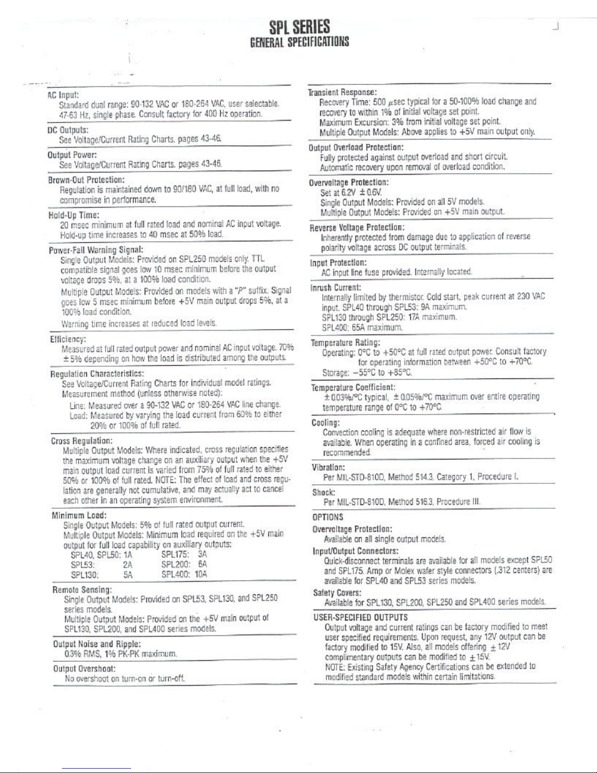
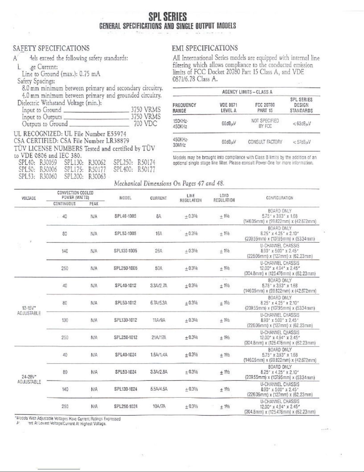
switching supplies (SPL250-1012) rated at 21 amperes are used to supply the GaAs FET Amplifier Modules
with power.
Page 6

ITS-5523
THEORY OF OPERATION - Continued
AC Voltage Source
The transmitter may be configured to be powered by either a 115 VAC/60Hz or 230 VAC/50Hz by the
following procedures.
230 VAC to 115 VAC Operation
Locate the 10 position terminal block (TB1) within the transmitter. Referring to Interconnect drawing 1555-
8102, remove the jumper between positions 2A and 3A. Remove the jumper between p ositions 4A and 5A.
remove VR1 (250V), VR2 (275V), and VR4 (275V) from terminal block TB1. Connect a jumper between
positions 3A and 4A. Connect another jumper between positions 5A and 6A. Move the jumper wire from
the 230 VAC terminal of the + 12VDC switching power supplies (A9 and A19) to the 115VAC terminal.
Install VR3 (150V) across positions 1A and 6A. Install VR4 (150V) across positions 1A and 3A.
115 VAC to 230 VAC Operation
Locate the 10 position terminal block (TB1) within the transmitter. Referring to Interconnect drawing 1555-
8102, remove the jumper between position 3A and 4A. Remove the jumper between positions 5A and 6A.
remove VR1 (130V), VR2 (150V), VR3 (150V), and VR4 (150V) from terminal block TB1. Connect a jumper
between position 2A and 3A. connect another jumper between positions 4A and 5A. Move the jumper wire
from the 115 VAC terminal of the +12 VDC switching power supplies (A9 and A19) to the 230 VAC terminal.
Install VR1 (250V) across positions 8A and 10A. Install VR2 (275V) across positions 3A and 6A. Install VR3
(275) across positions 1A and 3A.
Page 7

ITS-5523 DIGITAL TRANSMITTER TRAY (11555-1102)
SPECIFICATIONS
Technical Specifications
Type of Emissions...........................................................................................................................6M00D7W
Frequency Range............................................2150 to 2162 and 2500 to 2686 MHz (any 6 MHz channel)
Output Power Rating.......................................................................................... 5 to 10 watts total average
DC voltage and total current of final amplifier stage........................................... 10 volts DC at 24 amps
(Class A - Not RF power dependent)
Performance Specifications
Operating Frequency Range................................................................2150 to 2162 and 2500 to 2686 MHz
RF output - Nominal:
Power........................................................................................ 5 to 10 watts average (adjustable)
Impedance.............................................................................................................................50 ohms
Connector...............................................................................................................................Type N
Input: (Digital QAM) ...........................................................................................................................44 MHz
Out-of-Band Power..........................................................................................-38 dB max (at channel edge)
-60 dB max (0.5 MHz above channel edge and 1.0 MHz below channel edge)
Harmonic Products...........................................................................................................................-60 dB max
Electrical Requirements
Power Line Voltage.................................................................................................117 VAC, ±10%, 60 Hz or
220 VAC ±10%, 50 Hz
Power Consumption...........................................................................................................................175 watts
Environmental
Maximum Altitude............................................................................................................12,000 feet (3,660m)
Ambient Temperature.......................................................................................................................0° to 50°C
Mechanical
Dimensions: (WxDxH)..........................................................19" x 21" x 8.75" (48.3cm x 53.3cm x 22.24cm)
Weight: ................................................................................................................................... 30 lbs. (13.6 kgs)
Page 8

ITS-5523
FRONT PANEL METER, CONTROLS, AND LED INDICATORS
The ITS-5523 front panel provides operating controllability, metering capability and status indication. These features
provide an effective means to determine the over -all operating status of the transmitter at a glance.
Controls
ON/OFF (Rear Panel) Provides control of AC to the tray as well as circuit
protection.
OPERATE (DS2) Places transmitter into the Operate mode.
STANDBY (DS1) Places transmitter into the Standby mode.
A front panel meter is provided to monitor two levels. A rotary switch, located next to the meter, is used
to select the following metered parameters:
% FWD. PWR. (0-100%) Indicates percentage of output power (top scale).
% REFL. PWR. (0-100%) Indicates percentage of reflective power (top scale).
Status Indicators
Operating status indicators are provided for front panel viewing. From left to right they are:
PLL LOCKED (DS6)-GREEN Illumination indicates that the UHF generator is locked.
PLL REFERENCE PRESENT Illumination indicates that an internal or external reference
(DS4)-GREEN is present.
THERMAL INTERLOCK Illumination indicates that an over temperature fault is not
(DS3)-GREEN present in the amplifier
OUTPUT FAULT (DS7)-RED Illumination indicates that a fault condition exist.
OPERATE (DS2) Illumination indicates the transmitter is enabled.
STANDBY (DS3) Illumination indicates that the transmitter is disabled.
Page 9

ITS-5523
FRONT PANEL METER, CONTROLS, AND LED INDICATORS - Continued
One front panel label is provided for channel indication.
CHANNEL Indicates the operating channel.
Two front panel sample ports provide for monitoring specific RF levels:
CHANNEL OSCILLATOR Provides a sample from the channel oscillator. Nominal
sample level is - 3 dBm.
Page 10

ITS-5523
PRINTED CIRCUIT BOARD LED INDICATORS AND DESCRIPTIONS
There are both red and green LED indicators located within the transmitter. The green LEDs, when lit, show that the
function indicated is operating correctly. The red LEDs, when lit, show a malfunction of the function indicated.
______________________________________________________________________________
PRINTED CIRCUIT BOARD/LED DESCRIPTION
______________________________________________________________________________
ALC/AGC BOARD:
(DS2)-RED Illumination indicates that there is no IF signal present.
(DS3)-RED Illumination indicates that the ALC is out of range.
(DS5)-RED Illumination indicates that the IF signal is muted.
(DS4)-RED Illumination indicates that the AGC is out of range.
±12 VDC POWER SUPPLY BOARD:
(DS1)-GREEN Illumination indicates that U1 is supplying +12VDC to J3.
(DS2)-GREEN Illumination indicates that U2 is supplying +12VDC to J5.
(DS3)-GREEN Illumination indicates that U3 is supplying +12VDC to J4.
(DS4)-GREEN Illumination indicates that U4 is supplying +12VDC to J6.
(DS5)-GREEN Illuminatoion indicates that U5 is supplying +12VDC to J10.
(DS6)-GREEN Illumination indicates that U6 is supplying -12VDC to J7.
(DS7)-GREEN Illumination Indicates that U7 is supplying -5VDC to J8.
6 SECTION BIAS PROTECTION BOARD:
(DS1)-GREEN Illumination indicates that the Driver Amplifier and correction
amplifier are functioning properly.
(DS2 DS6)-GREEN Illumination indicates that the Output Amplifier
is functioning properly.
Page 11

ITS-5523
SYSTEM ALIGNMENT PROCEDURE
Connect a suitable load to the output of the Upconverter/Amplifier tray. Turn the circuit breaker (CB1)
located on the back of the tray to the on position. Place the Upconverter/Amplifier in standby by
pressing the standby switch on the front panel. The amber front panel indicator will light indicating that
the Upconverter/amplifier is in standby.
Connect the output of the CM720M Modulator tray (J5) to the IF Input of the Upconverter/Amplifier
tray (J2).
Make the connections and switch settings on each of the boards indicated below as follows.
IF Delay Equilizer Board (A3) Jumper from J1 to J2 (out of circuit)
Response Corrector Board (A5) S1 and S2 to out
ALC/AGC Board (A6) S1 and S2 to Manual
Linearity Corrector Board (A33) S1 to disable
Phase Corrector Board (A34) J9 and J10 to disable
Response corrector Board (A32) S1 and S2 to out
Place the Upconverter/Amplifier into operate by pressing the operate switch on the front panel. The
green front panel indicator will illuminate indicating that the Upconverter/Amplifier is in the operate
mode.
IF Amplifier Board (A1) 1521-1101
The IF Amplifier Board consist of a transformer coupled input for impedance matching to 50 O or 75 O
signals and a two stage amplifier providing about +24 dB of gain. Place W1 and W2 on pins 1 and 2 of
J10 and J11 (50O). Place jumpers W7 and W8 on pins 1 and 2 of J 12 and J13 (attenuator out). The output
of this board is approximately +6 dBm.
ALC/AGC Board (A6) 1022-1102
Disconnect J2. With SW1 and SW2 in the Manual position, adjust Manual ALC gain potentiometer R17
for about - 8 dBm at J2. Measure and record the voltage at TP3. Switch S1 to the ALC position.
Reconnect J2 and adjust ALC Gain potentiometer for the recorded voltage at TP3.
Using an appropriate directional coupler, connect a power meter to the RF output of the tray (J10).
Adjust Manual AGC potentiometer R101 for the rated output power (4 watts average) of the unit.
Dual Peak Detector Board (A22) 1522-1147
With the front panel selector switch in the Forward Power position, adjust Metering Adjust
potentiometer R101 for 100% on the front panel meter.
Page 12

ITS-5523
SYSTEM ALIGNMENT PROCEDURE - Continued
ALC/AGC Board (A6) 1022-1102
Adjust Inner Loop potentiometer R63 for 0.8 volts at TP7. Place switch SW2 into the AGC position.
Adjust AGC potentiometer R96 for 100% on the front panel meter.
Phase Corrector Board (A34) 1227-1250
The Phase Corrector Board corrects for phase non-linearities of the amplifier stages later in the system.
This board has been factory aligned and should not be adjusted without the proper equipment.
Response Corrector Board (A32) 1034-1205
Switch S1 and S2 into the in position.
Connect a sweep signal to the input of the Upconverter/Amplifier tray (J2). Monitor the output of the
Upconverter/Amplifier with a spectrum analyzer. Adjust C6, C7, and C8 for the frequency of the correction
notch being applied to response of the transmitter. R13, R15, and R17 are used to adjust the depth and
width of the correction notch. Adjust C6 and R13, C7 with R15, and C8 with R17 as needed to flatten the
response.
IF Delay Equalizer Board (A3) 1165-1018
The IF Delay Equalizer Board contains two sections of delay equalization that compensates for the
group delay created by external band pass filters (waveguide) and should not be adjusted without the
proper test set-up and equipment.
The IF enters the board at J1 and is applied to first section of the IF Delay Equalizer Board. The delay
equalizer is adjusted by removing W1 on J5 and tuning L1 for a notch at center frequency. Replace W1
and adjust C8 for the best response. The output of the first section at J2 connects to the input of the
second section at J3. The second section of the group delay equalizer circuit is adjusted by removing W2
on J6 and tuning L2 for a notch at center frequency. Replace W2 and adjust C10 for the best response.
VHF Generator Control Board (A14) 1519-1112
1. Disconnect the PLL reference frequency by removing the plug at J5 and/or J6.
2. Connect a digital voltmeter between TP4 (+) and ground (-). Adjust the manual bias potentiometer
(R87) for a reading of -3 VDC at TP4.
3. Connect a frequency counter to J11 to measure the VHF frequency (if frequency adjustments are
necessary, follow the above procedure for the UHF Generator board).
4. Set PLL programming per required channel frequency (See programming chart on following page).
5. Connect an oscilloscope between pin 28 of U2 or TP9 (+) and ground (-).
6. Reconnect the plugs at J5 and/or J6 and minimize the spike amplitude that will be observed on the
oscilloscope using the phase detector balance potentiometer R70.
Page 13

ITS-5523
SYSTEM ALIGNMENT PROCEDURE – Continued
UHF Generator Board (A15-A1) 1512-1101
1. Connect the main output from the channel oscillator section of the UHF Generator Board (J1) to a
spectrum analyzer, tuned to the crystal frequency and peak the tuning capacitors C6 and C11 for
maximum output. Tune L3 and L2 for maximum output. The output level should be +5 dBm ±2 dB.
While monitoring with a DVM, maximize each of the following test point voltages by tuning the
broadband multipliers in sequence.
2. Monitor TP1: Tune C32 for maximum (Typical 0.6 VDC).
Monitor TP2: Tune C34 and C38 for maximum (Typical 1.2 VDC).
Monitor TP3: Tune C40 and C44 for maximum (Typical 2.0 VDC).
Monitor TP4: Tune C46 for maximum.
Monitor TP4: Re-peak C38, C40, C44 and C46 (Typical 3.5 VDC).
3. Connect a spectrum analyzer, tuned to 8 times the crystal frequency, to the UHF Generator
output (J3). Monitor the output while peaking the tuning capacitors for maximum output.
4. The output level at J2 should be +15 dBm ±2 dB.
x3 Multiplier (A16) 1003-1004
1. While monitoring the x3 output (24 times the crystal frequency) with a spectrum analyzer, peak the
four tuning capacitor for maximum output. Typical output is about +3 dBm ±2 dB.
The output of the x3 Multiplier is fed to the input of the Upconverter Board.
Page 14

MMDS PROGRAMMING CHART FOR VHF GENERATOR CONTROL BOARD (1555-1214)
OSCILLATOR (1 = HIGH)
VISUAL L.0. = FREQUENCY = (0 = LOW)
CHANNEL CARRIER (FV+45.75 (L.O./24
NUMBER (MHz) MHz) MHz) (S1) (S2) (S3) (S4)
A1 2501.25 2547.00 106.125 1101 1000 1100 1111
A2 2513.25 2559.00 106.625 1111 1000 1100 1101
A3 2525.25 2571.00 107.125 1100 0100 1100 1110
A4 2537.25 2583.00 107.625 1110 0100 1100 1100
B1 2507.25 2553.00 106.375 1011 1000 1100 1011
B2 2519.25 2565.00 106.875 1000 0100 1100 1001
B3 2531.25 2577.00 107.375 1010 0100 1100 1010
B4 2543.25 2589.00 107.875 1001 0100 1100 1000
C1 2549.25 2595.00 108.125 0101 0100 1100 1111
C2 2561.25 2607.00 108.625 0111 0100 1100 1101
C3 2573.25 2619.00 109.125 0100 1100 1100 1110
C4 2585.25 2631.00 109.625 0110 1100 1100 1100
D1 2555.25 2601.00 108.375 0011 0100 1100 1011
D2 2567.25 2613.00 108.875 0000 1100 1100 1001
D3 2579.25 2625.00 109.375 0010 1100 1100 1010
D4 2591.25 2637.00 109.875 0001 1100 1100 1000
E1 2597.25 2643.00 110.125 1001 1100 1100 1111
E2 2609.25 2655.00 110.625 1011 1100 1100 1101
E3 2621.25 2667.00 111.125 1000 0010 1100 1110
E4 2633.25 2679.00 111.625 1010 0010 1100 1100
F1 2603.25 2649.00 110.375 1101 1100 1100 1011
F2 2615.25 2661.00 110.875 1111 1100 1100 1001
F3 2627.25 2673.00 111.375 1100 0010 1100 1010
F4 2639.25 2685.00 111.875 1110 0010 1100 1000
G1 2645.25 2691.00 112.125 0001 0010 1100 1111
G2 2657.25 2703.00 112.625 0011 0010 1100 1101
G3 2669.25 2715.00 113.125 0000 1010 1100 1110
G4 2681.25 2727.00 113.625 0010 1010 1100 1100
H1 2651.25 2697.00 112.375 0101 0010 1100 1011
H2 2663.25 2709.00 112.875 0111 0010 1100 1001
H3 2675.25 2721.00 113.375 0100 1010 1100 1010
NOTE: ON SWI TCHES S1, S2, S3 AND S4. THE HIGH (1) AND LOW (0) SETTINGS ARE READ AS
MARKED ON THE CIRCUIT BOARD.
Page 15

MDS PROGRAMMING CHART FOR VHF GENERATOR CONTROL BOARD (1555-1214)
OSCILLATOR (1 = HIGH)
VISUAL L.0. = FREQUENCY = (0 = LOW)
CHANNEL CARRIER (FV+44.75 (L.O./24
NUMBER (MHz) MHz) MHz) (S1) (S2) (S3) (S4)
MDS1 2151.25 2196.00 87.875 1100 1001 0100 1000
MDS2 2157.25 2203.00 88.125 0010 1001 0100 1111
Page 16

ITS-5523
SYSTEM ALIGNMENT PROCEDURE – Continued
Upconverter Board (A4) 1519-1125
This board does not contain any RF tuning adjustments. The Upconverter Module produces an RF output at
J2 by mixing two input signals (L.O. and I.F.) which are applied to J1 and J4 respectively.
The L.O. signal (+3 dBm) enters the module at J1 and is split into (2) separate and equal signals by a
Wilkinson splitter. One output from the splitter is amplified to provide a buffered output sample (0 dBm) at J3.
The second output from the splitter is also amplified and applied to the input of a mixer.
The IF signal enters the module at J4 and is applied to the input of a mixer. The output of the mixer produces
a difference signal (L.O - IF) which is then amplified and sent to the to the RF output jack J2 (+4 dBm). The RF
output from the board is sent a four section cavity filter.
Biasing for the amplifier stages is accomplished by the setting of potentiometers.
The board receives DC power (-5 VDC and +12 VDC) from an external source. +5VDC is produced on the
board by applying +12 VDC to the input of + 5VDC regulator.
Four Section w/Trap Cavity Filter (A15) 2000-1240
This filter has been factory swept for a 6 MHz bandwidth and should not be tuned without proper equipment.
The filter has a typical loss of approximately 3 dB. The output of the filter is sent to a three stage amplifier
module.
Three Stage Amplifier Module (A10-A1) 1516-1108
This amplifier does not contain any RF tuning adjustments. The module contains three cascaded
broadband GaAsFET amplifier stages (FLL101ME driving a FLL351ME driving a FLL2001-3) providing a
nominal gain of 36 dB. The operating current for each device (Q101, Q201, Q301) is controlled by a pot
mounted on a bias board within the module and can be set by measuring the voltage drop across the across
the .05 ohm resister (R1) on the Seven Section Bias Protection Board (A20) for Q301, and the voltage drops
across R14, and R15 (0.22Ω) on the Drain Daughter Board (1516-1114) for Q101 and Q201 respectfully.
1. With no RF signal applied and with the transmitter off, unsolder the drain leads located near the ferrite
beads of Q201 and Q301 on the drain Daughter Board (1516-1120). Connect a digital voltmeter across R14
on the drain Daughter Board. Apply AC power to the transmitter and place the transmitter into the Operate
mode.
2. Adjust the bias control (R103) for a reading of .04V across R14 on the drain Daughter Board (1516-1120).
This voltage represents a bias current of .18 amps on Q101.
3. Place the transmitter into the standby mode and then turn the transmitter off. Unsolder the drain lead of
Q101 and resolder the drain lead of Q201. Apply AC power to the transmitter and place the transmitter into
the Operate mode. Adjust the bias control (R203) for a reading of .16V across R15 on the drain Daughter
Board. This voltage represents a bias current of .720 amps on Q201.
4. Place the transmitter into the standby mode and then turn the transmitter off. Resolder the drain leads of
Q101 and Q301. Apply AC power to the transmitter and place the transmitter into the Operate mode. Adjust
the bias control potentiometer R303 for a reading of .24V across R1 on the Seven Section Bias Protection
Board. This represents a bias current of 4.8 amps on Q301.
The output of this amplifier is fed to the 50 Watt Amplifier Module (A10-A1).
Page 17

ITS-5523
SYSTEM ALIGNMENT PROCEDURE – Continued
50 Watt Amplifier Module (A10-A3) 1512-1107
This Amplifier module does not contain any RF tuning adjustments. The module contains two cascaded broadband
GaAs FET amplifier stages (FLL200-3 driving four parallel FLL200-3 's) providing a nominal gain of 18 dB. The
operating current for each device (Q101, Q201, Q301, Q401,and Q501) is controlled by a pot mounted on a bias board
within the module, next to each corresponding FET, and can be set by measuring the voltage drop across the .05 Ω
resistors (R3, R4, R5, R6, and R43) on the bias protection board. See chart below.
______________________________________________________________________________
GaAs FET Potentiometer Bias Protection Voltage Across Drain
Transistor Adjustment Board Resistor Bias Protection Current
Resistor Calculated
_________________________________________________________________________________________
______
Q101 R902 R3 .24 4.8
Q201 R802 R4 .24 4.8
Q301 R902 R5 .24 4.8
Q401 R802 R6 .24 4.8
Q501 R902 R43 .24 4.8
______________________________________________________________________________
_
The output of this amplifier is sent through a circulator (A50), then to the RF input jack (J10) at the rear of the tray.
The voltages needed to operate the amplifier modules are provided by the +12V/21 amp switching supplies (A9 and
A10) and the ±12VDC Power Supply Board (A28) which produces the -5VDC bias voltage.
The -5VDC supply is non-adjustable with a regulated output. To prevent damage to the GaAs FET amplifiers, the
+12VDC Supplies will not turn on until the -5VDC bias supply is operating.
The +12VDC/21 amp switching, regulated power supplies do not require any adjustment.
Six Section Bias Protection Board (A20) 1555-1213
This board does not contain any RF tuning adjustments. Indicator DS1 will illuminate if the amplifier circuits are
operating correctly with normal biasing and operating voltages.
Page 18

ITS-5523
REAR PANEL CONNECTIONS
The rear panel of the ITS-5523 provides quick and easy access to all of the external connections necessary to
interface the transmitter to the outside world.
CONNECTOR CONNECTOR
NUMBER TYPE
AC . . . . J1 . IEC . Provides AC input to the
transmitter
IF INPUT . . . J2 . BNC . Provides an external IF input from
the MMDS Receiver tray (50 Ω
impedance)
L.O. OUTPUT . . . J6 . BNC . Provides an L.O. output to a
Modulator.
EXT. 10 MHz REF. INPUT . J7 . BNC . Provides an external input to precisely phase
lock the L.O. to an external
reference (50 Ω impedance)
CONTROL . . . J12 . 37 Pos. Provides access to remote control
Female "D" functions of the booster.
REMOTE . . . J16 and J17. RJ45 Provides access to remote status
and
metering functions of the booster.
RF OUTPUT . . . J8 . "N" . Provides the RF output from the
tray. (50 Ω impedance)
Page 19

ITS-5523
REMOTE CONTROL INTERFACE
All remote/control functions are accessed through a 37 position "D" connector (J12) and two RJ45 connectors (J16
and J17) located on the rear panel of the Upconverter/Amplifier.
CONNECTION
Control:
REMOTE OPERATE . . . . . . . J16
REMOTE STANDBY . . . . . . . J16
EXTERNAL OPERATE COMMAND . . . . . J12
Metering:
FWD POWER . . . . . . . . J16
REFL POWER . . . . . . . . J16
ALC INPUT . . . . . . . . J12
Status:
REMOTE OPERATE . . . . . . . J16
TRANSMITTER INTERLOCK . . . . . . J12
TRANSMITTER FAULT . . . . . . J16
OVERTEMP . . . . . . . J16
Page 20

ITS-5523
DIGITAL TRANSMITTER
DRAWING LIST
UPCONVERTER/AMPLIFIER TRAY
The UPCONVERTER/AMPLIFIER TRAY consist of the following boards/modules:
x3 Multiplier Assembly.....................................................................................................................................................1003-1004
UHF Generator Board ....................................................................................................................................................... 1512-1101
Schematic.......................................................................................................................................................................1512-3101
50 Watt Output Amplifier Module..................................................................................................................................1512-1107
Schematic.......................................................................................................................................................................1512-3107
+12 VDC Power Supply Board.........................................................................................................................................1512-1119
Schematic.......................................................................................................................................................................1512-3119
Dual Peak Detector Board................................................................................................................................................1512-1147
Schematic.......................................................................................................................................................................1512-3147
Three Stage 10W Amplifier Module...............................................................................................................................1516-1108
Schematic.......................................................................................................................................................................1516-3108
±12VDC Power Supply Board..........................................................................................................................................1516-1145
Schematic.......................................................................................................................................................................1516-3145
Six Section Bias Protection Board...................................................................................................................................1519-1136
Schematic.......................................................................................................................................................................1519-3136
VHF Generator Control Board ......................................................................................................................................... 1555-1112
Schematic.......................................................................................................................................................................1555-3112
Transmitter Control Board ............................................................................................................................................... 1555-1102
Schematic.......................................................................................................................................................................1555-3102
ALC/AGC Board................................................................................................................................................................1022-1102
Schematic.......................................................................................................................................................................1022-3102
IF Input Equalizer Board...................................................................................................................................................1555-1219
Schematic.......................................................................................................................................................................1555-3219
Linearity Equalizer Board ................................................................................................................................................. 1034-1201
Schematic.......................................................................................................................................................................1034-3201
Visual Response Corrector Board...................................................................................................................................1034-1205
Schematic.......................................................................................................................................................................1034-3205
IF Delay Equalizer Board (45.75 MHz) ...........................................................................................................................1165-1018
Schematic.......................................................................................................................................................................1165-3018
Page 21

ITS-5523
DIGITAL TRANSMITTER
DRAWING LIST
UPCONVERTER/AMPLIFIER TRAY
Upconverter Board............................................................................................................................................................1555-1225
Schematic.......................................................................................................................................................................1555-3225
SCADA Controller Board.................................................................................................................................................1519-1107
Schematic.......................................................................................................................................................................1519-3107
Scada Connector Board....................................................................................................................................................1519-1102
Schematic.......................................................................................................................................................................1519-3102
IF Phase Corrector Board.................................................................................................................................................1227-1250
Schematic.......................................................................................................................................................................1227-3250
UHF Amplifier Board ........................................................................................................................................................ 1506-1206
Schematic.......................................................................................................................................................................1506-3206
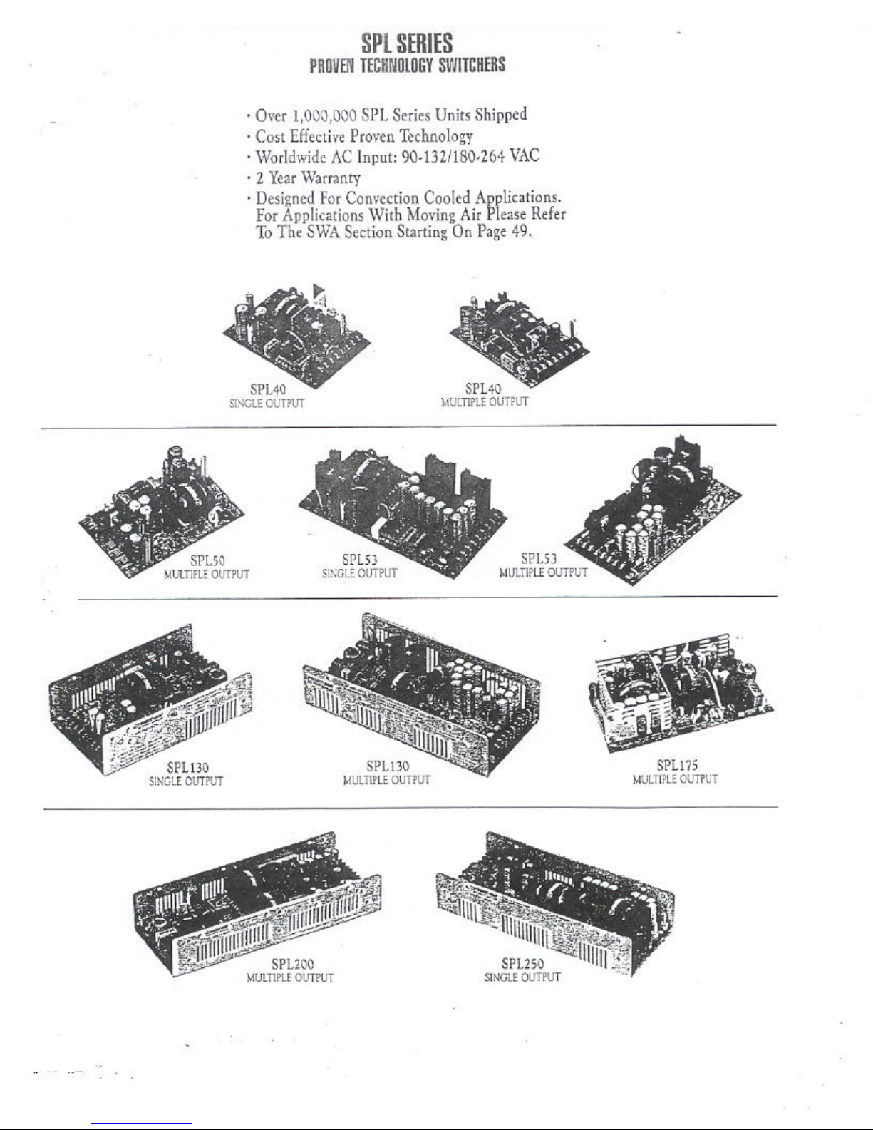
+12V/21A (250W) Switching Power supply.............................................................................................................SPL250-1012
Page 22
Page 23
Page 24
Page 25

MAINTENANCE AND TROUBLESHOOTING
Problem Analysis
In most cases, the performance of a GaAsFET transistor is closely tied to the DC operation of the system. Any
degradation in signal quality, gain or power is usually related to a corresponding change in a DC parameter
somewhere in the system. An exception may be a defective RF input or output connection, which can result in poor
performance of the amplifier with all DC parameters appearing normal.
The first step of analysis is therefore to carefully measure all DC parameters and compare these to the numbers
indicated on the schematics, block diagrams, and factory test data sheet. Each GaAsFE T operates with – .5V of bias
on the gate and about +10.2V maximum volts on the drain. The static current of a GaAsFET is determined by
measuring across associated .05 ohm resistor, located on the bias protection board and using Ohm’s Law .
If all DC parameters are normal, an RF intermittency should be suspected. Follow the RF path from input to output
and apply a small physical force on all connectors while observing the output power. If an intermittency is detected, a
simple re-soldering can be attempted.
While following these procedures, it is important to maintain terminations on all amplifier circuits to avoid VSWR
damage. Before a fan fails, it normally begins to exhibit noisy operation. Always check for free fan blade movement
and procure a replacement fan if fan-bearing noise is evident.
Repair Procedures
Repair of this transmitter normally involves module level replacement. ITS Corporation maintains an adequate stock
of replacement modules. If you have determined that a particular subassembly is defective and that it cannot be
easily repaired at your facility, please contact the ITS Customer Services Department. An effort will be made to
provide a module on an exchange basis. It is often possible to ship replacement modules counter-to-counter or oneday UPS/Federal Express to expedite delivery.
On some occasions it is necessary to perform component level repairs. In many cases failures can be a result of poor
connections somewhere in the system. Poor connections can generally be repaired with a suitable, small, grounded
soldering iron. A spare parts kit of standard components is available for this booster. Please contact the ITS
Marketing Department for the price and availability of the spare parts kit. Individual components can also be ordered
from the Customer Services or Marketing departments of ITS. The fuses are standard and generally available at local
parts distributors. The parts list provides complete manufacturer's information and part number for all standard
electrical components. These components can often be obtained from local distributors. An effort has been made to
select standard (off-the-shelf) components whenever possible in the product design. Replacement of the GaAsFET
transistors in the field is not recommended unless performed by an experienced technician. It is important to realize
that each GaAs FET operates at a specific bias voltage that must be preset before the main power supply is switched
on. Failure to provide the proper bias voltage will result in rapid GaAsFET destruction. Please refer to the ITS
Warranty and Material Return Authorization procedures for additional information concerning repair parts.
Periodic Procedures
This transmitter is designed with components that require no periodic maintenance except for cleaning and record
keeping.
Page 26

The amount of cleaning necessary depends greatly on the conditions in the translator room. While the electronics
have been designed to function well even if covered with dust, heavy buildups of dirt and insects will impede the
effectiveness of the cooling and lead to shutdown or premature failure.
When it is apparent that the front panel is becoming dust covered, the top cover should be opened and the
accumulated foreign material removed. A small, soft brush used in conjunction with a plastic wand-like attachment on
a small vacuum cleaner is an excellent way to remove dirt. Alcohol and other cleaning agents should not be used
unless you are certain that the solvents will not damage components or markings. Water based cleaners can be used
if only a small amount of moisture is used. The fans or heat sinks should be carefully cleaned.
Occasionally check that all RF connections are secure, but be careful not to over -tighten.
Data should be recorded for all meter readings on a regular basis. It is suggested that data be recorded once each
month and that it be retained in a rugged folder or envelope for the life of the equipme nt. A sample format of a log
sheet is included at the end of this section. Photocopies of this sheet may be used for if desired.
 Loading...