

Page 1
Riva Edge Mini HW Design and User Guide Rev 1.01
ITRON PROPRIETARY & CONFIDENTIAL INFORMATION
For Reference Only, Printed: 3/6/2018
Page 1 of 49
Program: Idea Labs Itron Riva Dev Mini
Name: Itron Riva Dev Mini Hardware User Guide
Compliance Information (Certification Exhibit) – For further
information see Appendix A.:
FCC ID: 2ANHYMINI1
FCC Rule Part: 15.247
Model: Itron Riva Dev Mini
Part Number: 575188r3
Manufacturer: Itron Inc
2111 N Molter Rd
LIBERTY LAKE WA 99019-9469
P: +1509.9249900
Page 2

Riva Edge Mini HW Design and User Guide Rev 1.01
ITRON PROPRIETARY & CONFIDENTIAL INFORMATION
For Reference Only, Printed: 3/6/2018
Page 2 of 49
Contents
Contents ........................................................................................................................................................................ 2
List of Tables .............................................................................................................................................................................. 4
Change List ................................................................................................................................................................................. 5
Introduction ............................................................................................................................................................................... 6
Purpose of Document ............................................................................................................................................................ 7
Definitions and Acronyms.................................................................................................................................................... 9
Reference Documents ............................................................................................................................................................ 9
Itron Riva Dev Mini Introduction .................................................................................................................................... 10
Itron Riva Dev Mini Board Description ........................................................................................................................ 11
Mechanical ........................................................................................................................................................................... 12
Major Components ........................................................................................................................................................... 12
CPU Brief .............................................................................................................................................................................. 12
Clocking ............................................................................................................................................................................ 12
FLASH And RAM Brief ..................................................................................................................................................... 12
RTC Brief .............................................................................................................................................................................. 13
PIC Brief ................................................................................................................................................................................ 13
PMIC Brief ............................................................................................................................................................................ 13
Itron Riva Dev Mini Power Handling ............................................................................................................................. 14
Power Input ........................................................................................................................................................................ 14
+5 VDC supply ............................................................................................................................................................... 14
+5 VDC from USB ..................................................................................................................................................... 14
+5 VDC from Expansion Header ....................................................................................................................... 14
Power Output ..................................................................................................................................................................... 14
+5 VDC to USB .......................................................................................................................................................... 14
+3.3 VDC supply To Expansion Connector (3V3_EXP) ................................................................................. 14
User Power Supply Warning ................................................................................................................................... 14
SYS_BOOT Configuration Jumpers ............................................................................................................................. 15
Startup – Riva Itron Riva Dev Mini Linux First Time Power On ........................................................................ 16
direct Wiring, No Solderless Breadboard Expansion Board ........................................................................... 16
Power Supplies ............................................................................................................................................................. 16
Create a console port .................................................................................................................................................. 16
Solderless Breadboard Expansion Board .................................................................................................................... 17
Itron Riva Dev Mini/NIC Test Fixture ...................................................................................................................... 18
Pogo-pin and socket Information (spring test pins) ............................................................................................... 19
Socket..................................................................................................................................................................................... 19
Pins ......................................................................................................................................................................................... 19
Page 3

Riva Edge Mini HW Design and User Guide Rev 1.01
ITRON PROPRIETARY & CONFIDENTIAL INFORMATION
For Reference Only, Printed: 3/6/2018
Page 3 of 49
Spear Pin .......................................................................................................................................................................... 19
Chisel Triad Pin ............................................................................................................................................................. 19
Cup Pin ............................................................................................................................................................................. 19
Establishing a Linux Session ............................................................................................................................................. 19
Get into a terminal ............................................................................................................................................................ 20
Getting a Prompt, and what to do with it ................................................................................................................ 20
Linux prompt ................................................................................................................................................................. 20
u-boot prompt ............................................................................................................................................................... 20
“C” stream (Continuous “C”s about 1 second apart) ..................................................................................... 20
No prompt at all ............................................................................................................................................................ 20
Pin Configuration and usage ........................................................................................................................................ 21
Itron Riva Dev Mini Pinout ........................................................................................................................................... 22
Expansion Connector Pinout Description ................................................................................................................... 22
Expansion Connector J4 Pinout .................................................................................................................................. 22
P4 Pin Descriptions ..................................................................................................................................................... 26
P4-1 and 2 +5.0 VDC ................................................................................................................................................... 26
P4-18 hv_cmp ................................................................................................................................................................ 26
P4-20 epf_IN* (This section requires work) ..................................................................................................... 27
P4-26 Battery................................................................................................................................................................. 28
P4-37 3V3_EXP .............................................................................................................................................................. 28
Expansion Peripheral Port Usage ................................................................................................................................... 28
SPI0 ......................................................................................................................................................................................... 28
SPI1 ......................................................................................................................................................................................... 28
AIN0...AIN3 .......................................................................................................................................................................... 28
I2C2 ........................................................................................................................................................................................ 29
DSP TO A8 Interconnects ................................................................................................................................................... 29
RF Connector and Cable ...................................................................................................................................................... 30
Downloading, If necessary (Linux) ................................................................................................................................ 31
Erasing FLASH Image ........................................................................................................................................................... 32
Erasing FLASH Image From u-boot ........................................................................................................................... 32
Erasing FLASH Image From Linux ............................................................................................................................. 32
Itron Riva Dev Mini Test Procedure .............................................................................................................................. 33
Equipment Required: ...................................................................................................................................................... 33
Minimal Operational Connections ............................................................................................................................. 33
Mini DK Test Fixture ................................................................................................................................................... 33
Mini DK Solderless Breadboard Adapter ........................................................................................................... 34
Mini DK Direct Wiring ................................................................................................................................................ 34
Smoke/Boot Test .............................................................................................................................................................. 35
Page 4

Riva Edge Mini HW Design and User Guide Rev 1.01
ITRON PROPRIETARY & CONFIDENTIAL INFORMATION
For Reference Only, Printed: 3/6/2018
Page 4 of 49
LED Testing .................................................................................................................................................................... 36
GPIO Testing................................................................................................................................................................... 36
Analog Input Pins ......................................................................................................................................................... 36
I2C2 Testing ................................................................................................................................................................... 37
SPI Testing ...................................................................................................................................................................... 39
UART0 Testing .............................................................................................................................................................. 40
USB1 Testing .................................................................................................................................................................. 40
EPF* Testing ................................................................................................................................................................... 40
HV_CMP Testing............................................................................................................................................................ 40
Battery Pin Testing ...................................................................................................................................................... 40
DSP Programming (Requires Fixture) .......................................................................................................................... 42
USB-To-Serial Adapters ...................................................................................................................................................... 45
USB Cables ................................................................................................................................................................................ 47
Appendix A: FCC Related Statements ............................................................................................................................ 48
OEM Labeling Requirements ....................................................................................................................................... 48
FCC Notices .......................................................................................................................................................................... 48
RF Exposure ........................................................................................................................................................................ 49
FCC-Approved Antennas (902-928 MHz) ............................................................................................................... 49
LIST OF TABLES
Figure 1: Top Side of Itron Riva Dev Mini showing iSOM ........................ Error! Bookmark not defined.
Figure 2: Bottom Side of Itron Riva Dev Mini ............................................... Error! Bookmark not defined.
Figure 3: Expansion Connector Pinout ......................................................................................................................... 11
Figure 4 - Revision 2 Itron Riva Dev Mini Board jumpers .................................................................................... 15
Figure 5 - ACT NIC on Solderless Breadboard Expansion Board ....................................................................... 17
Figure 6 - Itron Riva Dev Mini/NIC Test Fixture ...................................................................................................... 18
Figure 7 - FTDI TTL-232R-RPI ......................................................................................................................................... 45
Figure 8 - FTDI TTL232R-3V3-WE ................................................................................................................................. 46
Page 5

Riva Edge Mini HW Design and User Guide Rev 1.01
ITRON PROPRIETARY & CONFIDENTIAL INFORMATION
For Reference Only, Printed: 3/6/2018
Page 5 of 49
CHANGE LIST
Rev 0.07 –
1. Added RF cable information
2. Added Solderless Breadboard section
3. Added Test Fixture section
4. Updated revision number and table of contents
Rev 0.09 –
1. Added text to pin table
Rev 0.10 –
1. Added information about USB cables
2. Updated revision number and table of contents
Rev 0.11 –
1. Changed document name from ACT Dongle to Riva Edge Mini Dev Kit
2. Added testing section
3. Cleaned up other sections
Rev 0.12 –
1. Added DSP Programming section
Rev 0x13
1. Altered text in HV_CMP section
Rev 0x14
1. Updated pin out diagram for easier readability
2. Updated some text in Pinout description area
Rev 0.17
1. Corrected GPIO1_17 Table information
2. Added info on testing UART5
Rev 0.19
1. Switched Antenna and cables to reflect RP-SMA types
Rev 0.20
1. Enhanced Introduction section text.
Rev 0.21
1. Mentioned required pull-up resistors on I2C2_SCL_3.3 and I2C2_SDA_3.3
Rev 0.22
1. Added section on Expansion Connector J4 peripheral usage
Rev 1.0
1. APPENDIX A: FCC RELATED STATEMENTS added
2. 1
st
page edited with FCC related info (FCC ID, itd.)
3. Antenna info modified
Rev 1.01
1. RF Exposure statement added
Page 6
Riva Edge Mini HW Design and User Guide Rev 1.01
ITRON PROPRIETARY & CONFIDENTIAL INFORMATION
For Reference Only, Printed: 3/6/2018
Page 6 of 49
INTRODUCTION
The Itron Riva Dev Mini Kit is a complete Linux system on a module that includes an Itron ACT Radio
suitable for addition to an Itron ACT RF network. It contains all hardware and comes loaded with
firmware which allows the user to easily bring up a product within an ACT Network.
It is intended to be used in a laboratory environment for product development or used as a
professionally installed OEM module1.
The end user will be a hardware developer who will ensure a proper power supply, ESD protection,
physical enclosure, and antenna are provided to suit their product needs. The end user will also
provide customized firmware to suit their application.
Only specified antennas may be used for integration of the OEM module to comply with FCC emission
limits! Please refer to the antenna tables in this document. Antenna and RF Cable type and purchasing
information are provided later in the document.
If the product is used as an OEM device within a user’s product they will be responsible for all testing,
qualifications and specifications to insure the Mini DK operates within all agency certifications that
apply to the product. The end user is also responsible for all design related to safety designs and
testing of safety features.
Only specified antennas listed in this document may be used for integration of the OEM module to
comply with FCC emission limits! Please refer to the antenna tables in this document. Antenna and
RF Cable type and purchasing information are provided later in the document.
The Itron Riva Dev Mini is designed by Itron and based on an Itron iSOM module which is based on a
TI AM335X ARM Cortex Microprocessor. The iSOM module contains the processor, FLASH, RAM,
power supply control, clock and other features. This iSOM module is mounted to a small board which
includes all ACT RF circuitry to act as a USB NIC. There is also an expansion connector to allow the
board to serve as the control and communications part of assorted devices.
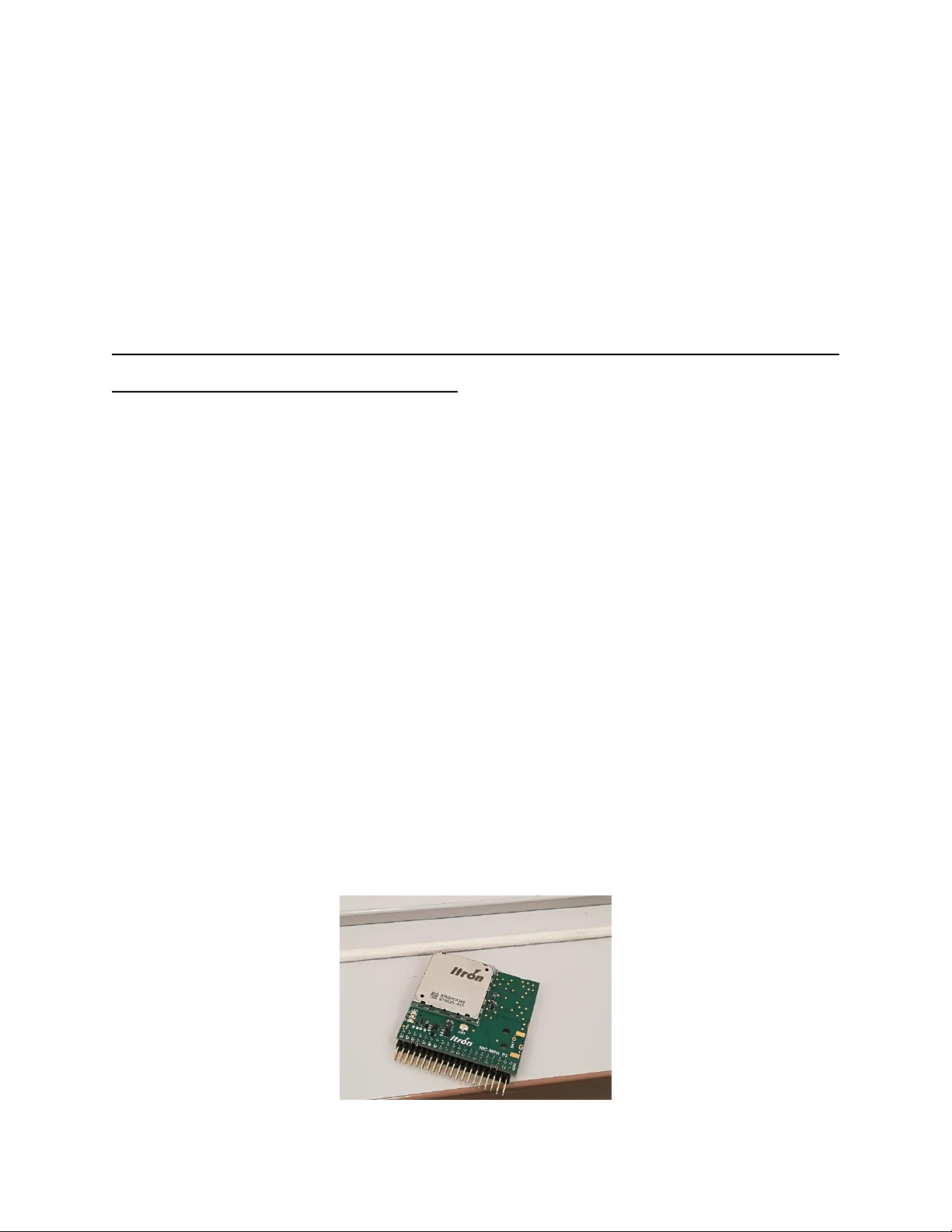
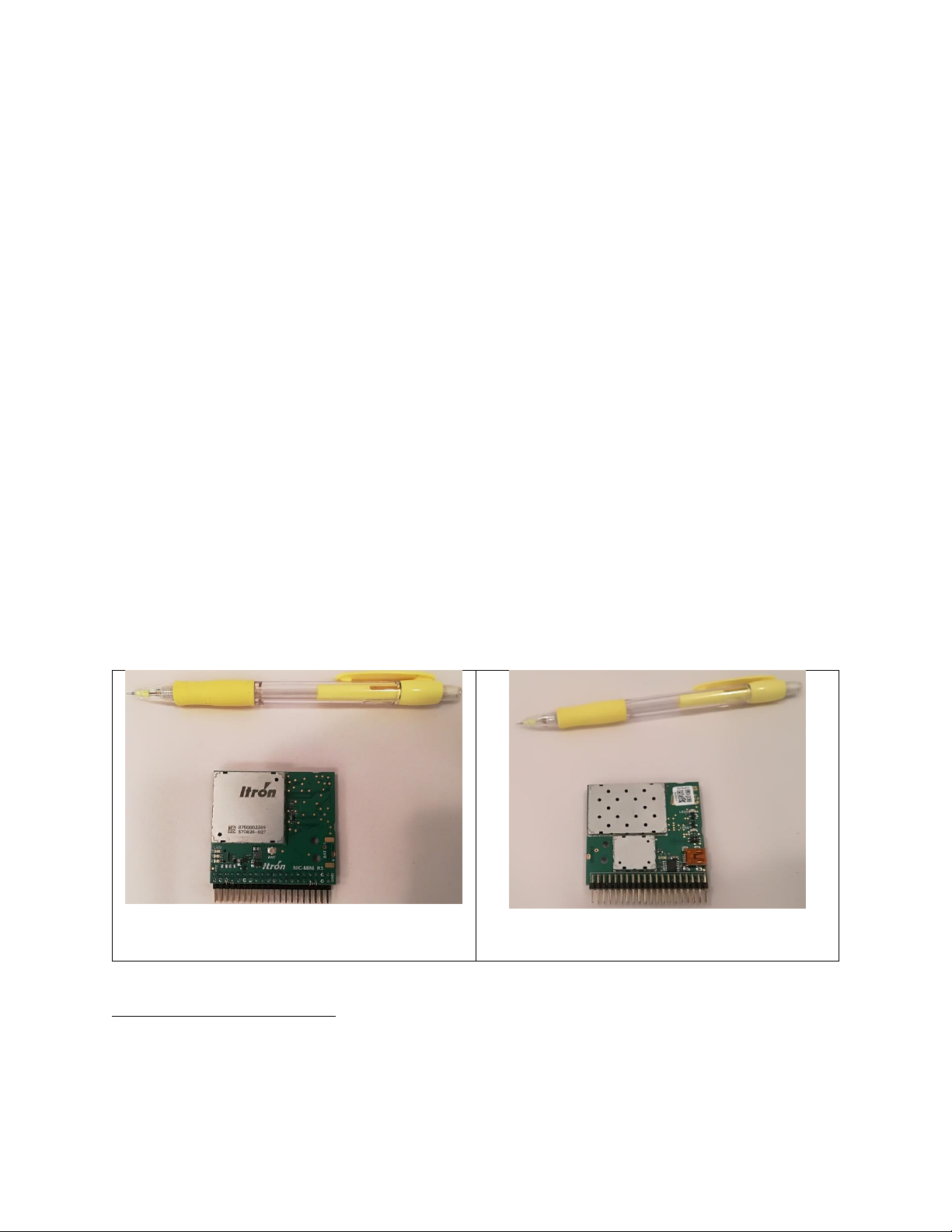
Figure 1: Top Side of Itron Riva Dev Mini showing
iSOM2
Figure 2: Bottom Side of Itron Riva Dev Mini3
1
Only specified antennas may be used for integration of the OEM module to comply with emission limits! Please
refer to the antenna tables in this document.
2
Note that 40 Pin connector is not place in this picture.
3
Note that 40 Pin connector is not place in this picture and that the shields are left off of the RF and DSP
sections.
Page 7

Riva Edge Mini HW Design and User Guide Rev 1.01
ITRON PROPRIETARY & CONFIDENTIAL INFORMATION
For Reference Only, Printed: 3/6/2018
Page 7 of 49
PURPOSE OF DOCUMENT
The goal of this document is to provide a hardware designer with enough information to use the Itron
Riva Dev Mini board as a processing engine for assorted types of projects. It will cover the hardware
necessary, at a high level, to guide a designer to the point where they can bring Linux up on the
platform.
This document is intended to show the user how to interface the Itron Riva Dev Mini to a product
based on the Muse platform. However, there will not be a comprehensive definition of how to use
each type of GPIO to interface to assorted devices. This will have to be obtained through the A8
datasheet. Some examples will be given but most of the time only the parameters of the pin will be
defined and its usage left up to the end product designer to reconfigure them as necessary. You may
contact Itron for specific interface assistance.
Building Linux will also be covered in a separate document.
This document is not intended to inform the user how to use Linux or any subset of Linux commands.
The coverage of Linux will only cover booting to a kernel prompt. This document is not intended to
be a detailed usage guide to Linux or to the intricacies of the additions that Itron has made to Linux
through its extensive IP library. These details are covered in separate documents.
This document is also will not cover Muse additions to the Linux Operating System or the Itron Over
the Air protocols or how to use them. Contact Itron for specific assistance in these areas.
Page 8

Riva Edge Mini HW Design and User Guide Rev 1.01
ITRON PROPRIETARY & CONFIDENTIAL INFORMATION
For Reference Only, Printed: 3/6/2018
Page 8 of 49
ESD Warning
ESD Warning
This product is intended to be treated as any other solid state component that you may use in an ESD
save engineering or manufacturing environment. Many exposed pins do not have any additional ESD
protection beyond what is provided by the integrated circuit that is directly connected to that pin.
Treat it as you would treat any other high density low voltage electronic component.
This product, like all microcontroller products, uses semiconductors that can be damaged by
electrostatic discharge (ESD). When handling, care must be taken so that the devices are not
damaged. Damage due to inappropriate handling is not covered by the warranty.
The following precautions must be taken:
•Do not open the protective conductive packaging until you have read the following, and are at an
approved anti-static work station.
•Use a conductive wrist strap attached to a good earth ground.
•If working on a prototyping board, use a soldering iron or station that is marked as ESD-safe.
•Always disconnect the microcontroller from the prototyping board when it is being worked on.
•Always discharge yourself by touching a grounded bare metal surface or approved anti-static mat
before picking up an ESD - sensitive electronic component.
•Use an approved anti-static mat to cover your work surface.
Page 9

Riva Edge Mini HW Design and User Guide Rev 1.01
ITRON PROPRIETARY & CONFIDENTIAL INFORMATION
For Reference Only, Printed: 3/6/2018
Page 9 of 49
DEFINITIONS AND ACRONYMS
Term
Definition
EPF
Early Power Fail
An indication to the Linux system that the
system requires a graceful shutdown.
HV_CMP
High Voltage Compare
This is the circuit name for the power fail
sense input to the PMIC. It is used to create
PDN_POWERFAIL to insure the rails are
shutdown with proper sequencing.
IP
Intellectual Property
For example, the extensions Itron has
created to extend the capabilities of the
platform in our products.
MMPS
Main Motherboard Power Supply
This is the main power supply for the
motherboard that the module is soldered to.
At times in this document it is also referred
to as +24VDC. This supply is the one that all
power rails and power control signals are
ultimately derived from.
PIC A Microchip microprocessor used to control
our power rails and provide other services to
the A8
PLC
Power Line Carrier or
Power Line Communications
A method of transmitting and receiving data
through the power lines.
PMIC
Power Management IC
This chip contains multiple switching and
LDO regulators and other power rail
management circuitry.
FTDI
Future Technology Devices
International LTD
Manufacturer of USB to Serial converter
cables
Itron Riva Dev
Mini
This board
Either of these two terms may be used to
describe this board depending on how it is
used.
ACT NIC
This board
REFERENCE DOCUMENTS
• A8 Product Preview Document. (SPRS717B.PDF)
• A8 Technical Reference Document (SPRUH73C)
• PIC16(L)F1824/8 Datasheet (DS40001419E)
• NXP PCF85363A RTC Datasheet
• CDP 3.02 PICInCircuitProgramming.docx
• Riva ACT-RF Design and User Guide
• DS_TTL-232R_CABLES.pdf
• SMSC 9514 USB 2.0 Hub and 10/100 Ethernet Controller Chip
Page 10
Riva Edge Mini HW Design and User Guide Rev 1.01
ITRON PROPRIETARY & CONFIDENTIAL INFORMATION
For Reference Only, Printed: 3/6/2018
Page 10 of 49
ITRON RIVA DEV MINI INTRODUCTION
This section describes, at a very high level, the nature of the Itron Riva Dev Mini which is based on
the Itron iSOM and includes ACT RF functionality to support the 870 MHz and the 920 MHz bands
used for the proprietary Openway network. The RF section connects to an antenna via a UF.L
connector4.
The Itron Riva Dev Mini has one mini-USB connector. Power can be derived from the external host
when the board is operating as a USB device. Power can be provided to a device when the board is
operating as a host. This is basic OTG operation but not certified as OTG by the USB group.
The Mini DK does NOT directly support Ethernet. An Ethernet port can be created by using a USB-toEthernet adapter.
The Itron Riva Dev Mini does NOT support EMMC or other external memory. It is possible to breakout J4 to provide a second USB port that can use USB based external memory such as a hard drive or
a thumb drive.
A 40 pin expansion connector is provided to bring control and communications off the board. The
pinout is shown below. This connector allows use of a standard ribbon cable to extend the signals to
another board.
4
Only specified antennas may be used for integration of the OEM module to comply with emission limits! Please
refer to the antenna tables in this document. RF Cable type and purchasing information is provided later in the
document.
Page 11

Riva Edge Mini HW Design and User Guide Rev 1.01
ITRON PROPRIETARY & CONFIDENTIAL INFORMATION
For Reference Only, Printed: 3/6/2018
Page 11 of 49
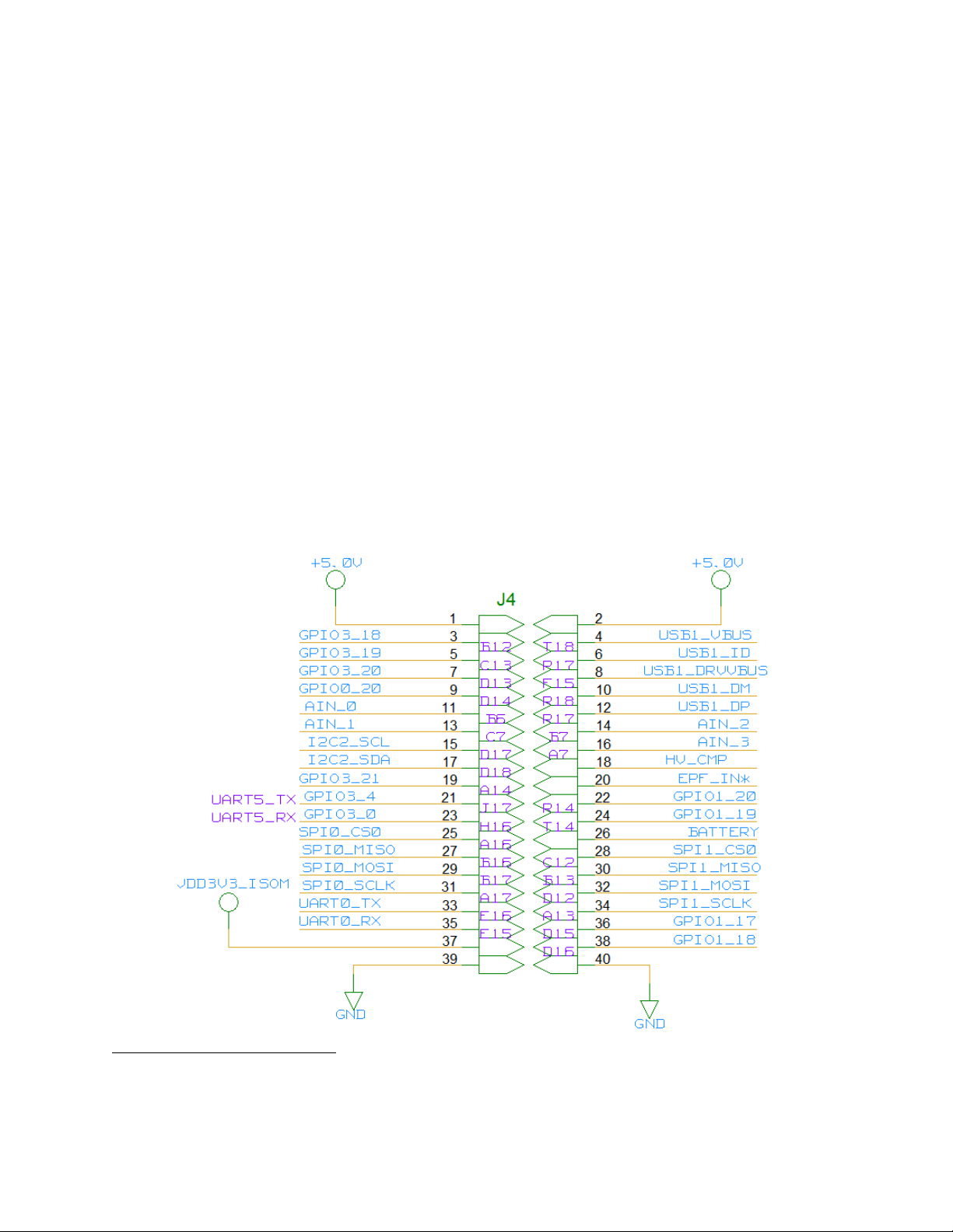
Figure 3: Expansion Connector Pinout
ITRON RIVA DEV MINI BOARD DESCRIPTION
The Itron Riva Dev Mini takes the Itron iSOM module, combines it with an ACT RF module and
expands it into a Complete Embedded Linux Communications system through an assortment of
communications and control lines on an expansion header. The board is designed to be used as a
development platform for embedded product prototyping or as the core processor NIC for an
embedded product.
Following is a list of the available hardware:
Item
Description
Notes
Single 5VDC supply
All other rails are generated on the module
A8 Microprocessor
ARM® Cortex™-A8 32Bit RISC
Microprocessor
32KB L1 Cache
256KB L2 Cache
Internal RAM
Dedicated to boot and
security
64KB Dedicated on-chip RAM
Internal RAM
General Purpose
64KB on chip RAM
Internal ROM
176K On-Chip boot ROM
Crypto Hardware
Accelerator
AES, SHA, PKA and RNB
External FLASH
2Gb as x16
Code, file system and data storage
External RAM
1Gb as x16
Data storage
EEPROM
256 Bytes
On PIC, accessible through I2C
RTC
NXP PCF85363A
Very Low Power
External Interrupts
Early Power Fail
Detection
For graceful Linux shutdown, Accessed
through the Expansion Connector
Expansion Signals
SPI0, SPI1
Accessed through the Expansion Connector
I2C2
Accessed through the Expansion Connector
UART1, UART4
Accessed through the Expansion Connector
Assorted GPIOs
Accessed through the Expansion Connector
AIN_0…AIN_3
4 ADC inputs, 12 Bits,
Accessed through the Expansion Connector
UART0
Linux Console
Accessed through the Expansion Connector
USB0
Mini-USB connector
USB1
Accessed through the Expansion Connector
JTAG
Bottom of board Test Points marked JTAG
PIC interface
PIC Programming
Bottom of board Test Points Marked JPIC
Page 12
Riva Edge Mini HW Design and User Guide Rev 1.01
ITRON PROPRIETARY & CONFIDENTIAL INFORMATION
For Reference Only, Printed: 3/6/2018
Page 12 of 49
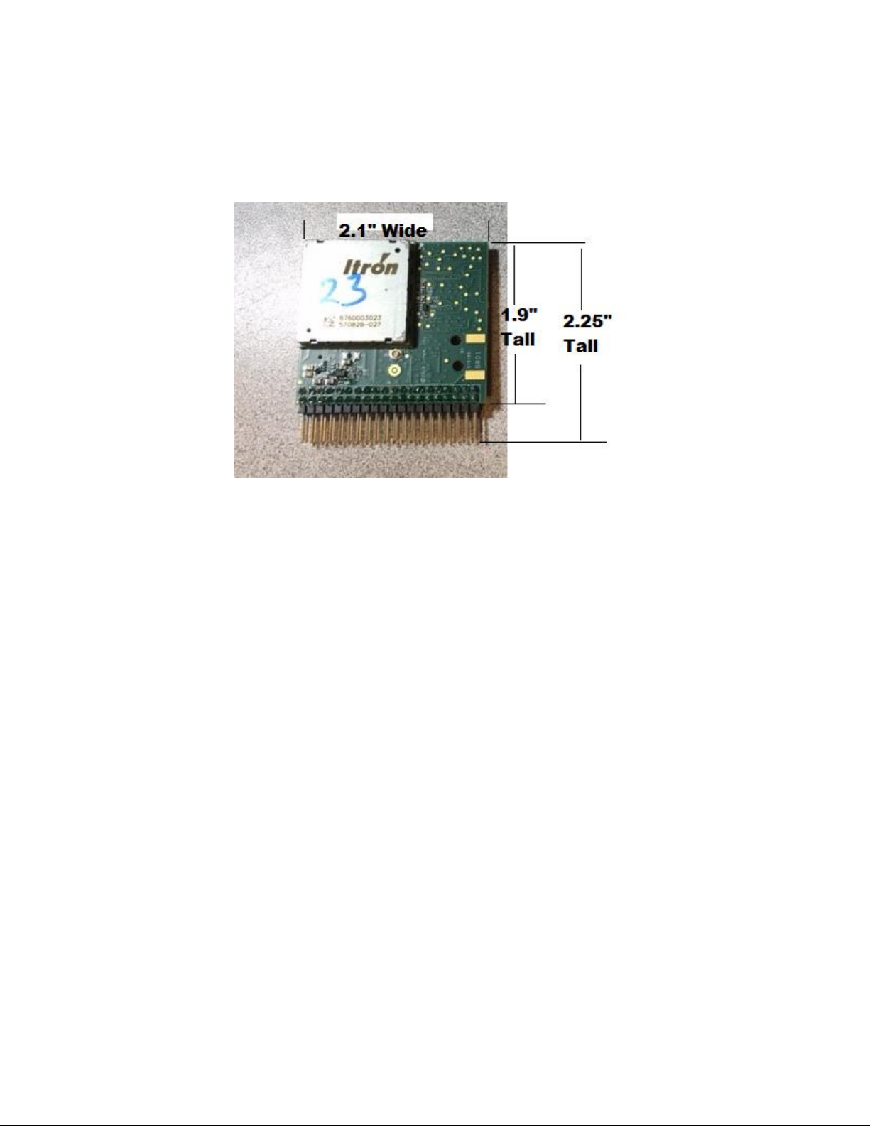
MECHANICAL
The Mini is a compact board designed for small environments. It is available with a vertical connector,
a right-angle connector or no connector. The connector can also be located on either side of the board
to best suit a customer’s needs.
Figure 4: Mini Board Dimensions
MAJOR COMPONENTS
The following sections will list the major components on the Itron Riva Dev Mini and briefly describe
them. Datasheets are available for more detailed information.
Caution!! Only specified antennas listed in this document may be used for integration of the OEM
module to comply with FCC emission limits! Please refer to the antenna tables in this document.
Antenna and RF Cable type and purchasing information are provided later in the document.
CPU BRIEF
The Muse Platform contains a TI AM335X ARM Cortex Microprocessor. The processor contains a
number of internal peripherals such as UARTs, SPI, I2C, USB, MMC, RTC and others. It also contains
an internal boot ROM and internal RAM. The ROM and RAM are mostly used during the boot-up
process and during security operations.
CLOCKING
A 26MHz clock crystal is used to clock the AM335X. This is internally changed to 450 MHz using an
internal PLL through Firmware. Other speeds can be selected depending on user requirements.
FLASH AND RAM BRIEF
The system contains a Micron technologies MT29C2G24MAABAHAMD-5IT chip in a 130 ball package
combining both FLASH and RAM on single chip. The Itron PN is 570725-003. This is a 2Gb NAND
(x16bit) + 1Gb (x16bit) LPDDR.
Page 13

Riva Edge Mini HW Design and User Guide Rev 1.01
ITRON PROPRIETARY & CONFIDENTIAL INFORMATION
For Reference Only, Printed: 3/6/2018
Page 13 of 49
RTC BRIEF
The module contains a NXP PCF85363A RTC CHIP. It is a tiny Real-Time Clock/calendar with 64-byte
RAM, alarm function, battery switch over and I2C-bus.
PIC BRIEF
The module contains a Microchip PIC16LF1823, or PIC16LF1823 microprocessor to serve as the
power rail control and to provide some system support features.
The PIC provides
1. Power Rail control
2. PON timing
3. Reset capability for the A8
4. EEPROM and some configuration storage.
PMIC BRIEF
The TI TPS650250 PMIC provides 3.3VDC, 1.8VDC and 1.1VDC regulators to supply the requirements
for the A8, RAM, FLASH and other components.
The PMIC also provides two LDO regulators. One provides 3.3VDC to the PIC and the other provides
3.3VDC to the Real Time Clock chip5. The two LDO enables are hard wired to a MIC826 voltage
monitor chip and come on as soon as 5 VDC is applied to the module. The PIC will then sequence the
power rails to the A8 and other circuitry.
5
As of the writing of this document the RTC chip was being changed. The original chip was an AM1805. I do not
know what the new chip is at this time.
Page 14

Riva Edge Mini HW Design and User Guide Rev 1.01
ITRON PROPRIETARY & CONFIDENTIAL INFORMATION
For Reference Only, Printed: 3/6/2018
Page 14 of 49
ITRON RIVA DEV MINI POWER HANDLING
POWER INPUT
The Mini requires a single +5 VDC supply. The input voltage should be within 4.75 VDC and 5.25 VDC.
+5 VDC SUPPLY
The Itron Riva Dev Mini requires an input power supply of +5 VDC. This can be supplied through the
mini-USB connector or through the expansion connector. The +5.0 VDC supply derives from one of
two sources: U57, the mini-USB connector or from the expansion header pins 1 and 2. In either case
this board can consume a peak of about 6 watts during full power transmissions.
+5 VDC from USB
When the Itron Riva Dev Mini is powered through the mini-usb connector it will provide +5 VDC
power to the expansion connector pins 1 and 2. There is a circuit to limit the inrush current to prevent
the host from triggering an over-current error. Once the initial period of current limiting ends the
TPS2151 will allow up to 1.6 amps to flow from the USB Host. Note it is up the system firmware to
provide the configuration and protocol operations to request the maximum required current from
the host port. Careful attention to this detail must be followed for adding external circuitry.
+5 VDC from Expansion Header
If the mini-USB port is not used as a power source +5 VDC may be supplied through the expansion
connector pins 1 and 2. Currently, for the first prototype run, this will not provide power to the miniUSB port. It should be possible to put a diode where R21 is to allow powering the mini-usb from the
expansion +5 VDC input.
POWER OUTPUT
+5 VDC to USB
When powered from the USB connector the current limited +5 VDC is routed to the Expansion header
to provide power for additional circuitry.
+3.3 VDC SUPPLY TO EXPANSION CONNECTOR (3V3_EXP)
There is a 3.3 VDC regulator connected to the +5 VDC signal to create an expansion power supply for
use by the user. This rail is gated by a signal from the iSOM which tells the system that the iSOM is
powered on and ready. This supply rail is limited to 250ma.
USER POWER SUPPLY WARNING
When adding hardware to the interface connector it may be required to create additional power
supply rails or higher current supplies. It is important to not connect any of these voltages to the
Itron Riva Dev Mini before the A8 has its power rails in place and steady. Having a voltage on an I/O
Pin on the A8 before it has its Vdd supply can cause permanent damage to the A8.
If you need to create your own power supplies make sure you gate them with 3V3_EXP because
3V3_EXP will not rise until the A8 supply rails are ready. This will prevent you from damaging the A8
processor or other circuitry.
Page 15
Riva Edge Mini HW Design and User Guide Rev 1.01
ITRON PROPRIETARY & CONFIDENTIAL INFORMATION
For Reference Only, Printed: 3/6/2018
Page 15 of 49
SYS_BOOT CONFIGURATION JUMPERS
The board comes configured to run its preloaded Linux on delivery. It is rarely necessary to change
the configuration jumper or switches.
The A8 can boot from a number of peripherals or memory units. For instance, it can boot from a
UART, USB, I2C, NAND or other sources. Often first stage of booting is used to load a small bootloader
which will then download the full system code. The iSOM module brings two of the system boot
configuration pins out on its connector. The two signals are SYSBOOT0, on J1 pins 1 and 2, and
SYSBOOT4, on J1 pins 3 and 4.
Normally both jumpers will be in the off condition. But occasionally other modes may be required.
For instance, if a download was interrupted leaving bad contents in FLASH the system may appear
dead or not be presenting CCCC. You can configure Sysboot0 jumpered and Sysboot4 unjumpered to
not allow booting from NAND thereby forcing a boot from UART0. This will present CCCC allowing
you to xmodem the SPL file and then ymodem the u-boot program to get a u-boot prompt. Once at
the prompt a “nand erase.chip” will restore the flash to a blank state and a complete reload can be
started.
These two pins are connected to individual mini-jumpers and can be used together to determine the
boot sequence the A8 will use. Typically, the both jumpers are left in the open position.
Figure 5 - Revision 2 Itron Riva Dev Mini Board jumpers
Rev. 1
Boot Order
SYSBOOT4
J1 (3-4)
SYSBOOT0
J1 (1-2)
On = 0
Off = 0
UART0
SPI0
NAND
NANDI2C
A8 Sends Cs
On = 0
On = 1
EMAC1
MMC0
XIP
NAND
Off = 1
Off = 0
NAND
NANDI
USB0
UART0
DEFAULT
Off = 1
On = 1
MMC0
SPI0
UART0
USB0
Force CCC to allow xmodem of
spl + mlo to get to uboot to
erase nand.chip
Page 16

Riva Edge Mini HW Design and User Guide Rev 1.01
ITRON PROPRIETARY & CONFIDENTIAL INFORMATION
For Reference Only, Printed: 3/6/2018
Page 16 of 49
STARTUP – RIVA ITRON RIVA DEV MINI LINUX FIRST TIME POWER ON
This section covers powering the board on and getting a prompt at the command line. The
information below assumes you are starting with a fresh power-up having had your supply at 0VDC
previously. This is the absolute minimal step to get an operational Linux console.
When shipped from the Itron factory the board is programmed with MLO, u-boot and a valid kernel.
The PIC is also programmed. The two configuration jumpers are also placed in the basic operation
configuration. So on receipt the board should boot into Linux without any changes.
The board can be powered up by using several different methods;
1. Connecting to a solderless breadboard expansion board
2. By direct wiring
3. On a Test Fixture
4. By connecting to another host board.
The following sections explain these methods in detail. Item 4 is not covered because it implies the
user has developed their own host board.
DIRECT WIRING, NO SOLDERLESS BREADBOARD EXPANSION BOARD
Establishing a terminal session is a very simple process. Essentially only +5 VDC is required along
with a console serial port. This is the minimal requirements to boot into a Linux system.
POWER SUPPLIES
Connect +5 VDC through the expansion connector. Leave this turned off for now.
CREATE A CONSOLE PORT
Connect a USB-To-Serial adapter to J4. Some adapters do not require 3.3 VDC so Pin 37 may be
omitted based on the wiring guide provided by the USB adapter manufacturer. More information
about USB-To-Serial adapters is provided later in this document.
J4 Pin 33
UART0_TX
J4 Pin 35
UART0_RX
J4 Pin 37
3.3 VDC
J4 Pin 39
Ground
Page 17

Riva Edge Mini HW Design and User Guide Rev 1.01
ITRON PROPRIETARY & CONFIDENTIAL INFORMATION
For Reference Only, Printed: 3/6/2018
Page 17 of 49
SOLDERLESS BREADBOARD EXPANSION BOARD
The easiest way to connect and power the board is to use the solderless breadboard expansion board.
This board breaks the pins out spaced properly to allow the device to be plugged into a solderless
breadboard. Even if not being used with an actual breadboard it provides the typical +5 barrel
connector and 4-pin UART0 connection used on our development kits.
Figure 6 - ACT NIC on Solderless Breadboard Expansion Board
When inserting the Itron Riva Dev Mini/NIC into the expansion board be very careful of orientation.
Note that the mating connector on the expansion board has a label in each side noting which shield
should be visible and power orientation. The “iSOM side” is the side with a single square shield with
the large Itron logo printed on it and the 57088-027 part number. The last 3 digits of the part number
may vary depending on the iSOM configuration.
Simply plug the board into the expansion board, connect a +5 VDC power supply to the barrel
connector (center +) and a serial port to the 4-pin connector. The system is now ready to boot.
Page 18

Riva Edge Mini HW Design and User Guide Rev 1.01
ITRON PROPRIETARY & CONFIDENTIAL INFORMATION
For Reference Only, Printed: 3/6/2018
Page 18 of 49
ITRON RIVA DEV MINI/NIC TEST FIXTURE
A test fixture has been designed to support programming and testing of the Itron Riva Dev Mini/NIC.
Typically this will be an Itron factory item or an Itron development base. At this time, I do not know
if it will be made available to customers.
This fixture provides the following capabilities:
1. A8 UART0 breakout and Other UARTs
a. JM4 Breakout (40 Pin Expansion Connector) to LEDs and headers
2. A8 JTAG
3. DSP JTAG
4. USB1 Breakout and connector
5. +5 VDC Supply Connector
6. Miscellaneous test point breakout
There is a separate manual that describes this fixture in detail.
Figure 7 - Itron Riva Dev Mini/NIC Test Fixture
Page 19

Riva Edge Mini HW Design and User Guide Rev 1.01
ITRON PROPRIETARY & CONFIDENTIAL INFORMATION
For Reference Only, Printed: 3/6/2018
Page 19 of 49
POGO-PIN AND SOCKET INFORMATION (SPRING TEST PINS)
Pogo-pins are used for reliable temporary connection between the fixture and the Itron Riva Dev
Mini Under test.
Do not turn the fixture upside down without something to hold the pins in. By their nature the pins
slide in and out of the sockets easily. If you do turn a fixture upside down many, if not all, of the pogo
pins may fall out.
Note that it is nearly impossible to clamp a board onto the fixture with all pins inserted. We
recommend that you only insert the pins that are required for the particular function you are
performing. For instance, it is not necessary to insert all pins for DSP or A8 programming. Pin usage
is shown in the
following section including a map of pins by usage group for each function.
SOCKET
Sockets are used to hold the pogo-pins into the test fixture. They are soldered in but can be replaced.
Different types of pins may be inserted into the sockets as needed.
The pogo-pin socket is QA Technology Company art number 100-SDN2502 a “100 Socket, Sgl PR,
WireWrap”. This socket is press fit into the alignment block and then goes into a PCB hole. The pin is
soldered into the PCB. Because of the way these are mounted it is very difficult to remove or replace
a socket.
The best method is remove a socket is to heat the respective pin at the PCB until the solder melts.
Then pull the socket from the top of the alignment board through the alignment board.
PINS
Three types of pogo-pins are used for this fixture and one type of socket. Pins just slide into and out
of the sockets with no force needed.
SPEAR PIN
This spear pin type used to mate to test points on the Itron Riva Dev Mini PCB. Many useful signals
are brought out on test pins for diagnostics and programming. For instance, all usable GPIO are
brought out to LEDs so they can be flashed for testing. The QA Technology part number for the spear
pin compatible with this fixture is “100-PRN2541L”.
CHISEL TRIAD PIN
The Chisel Triad pin type used to mate to holes in the Itron Riva Dev Mini PCB. Often the fixture will
be used with a Itron Riva Dev Mini that does not have the 40 pin expansion connector populated. The
QA Technology part number for the chisel Triad pin compatible with this fixture is “100-PRN2518L”.
CUP PIN
This Cup pin type used to mate to through hole connectors on the Itron Riva Dev Mini PCB such as an
expansion connector has been soldered onto a board. Cup pins mate to the bottom of the connector
that protrudes through the bottom of the board. The QA Technology part number for the spear pin
compatible with this fixture is “100-PRN2522L”.
ESTABLISHING A LINUX SESSION
Page 20

Riva Edge Mini HW Design and User Guide Rev 1.01
ITRON PROPRIETARY & CONFIDENTIAL INFORMATION
For Reference Only, Printed: 3/6/2018
Page 20 of 49
GET INTO A TERMINAL
Establish a terminal using a terminal emulator application. This can be done from Windows with
something like Hyperterm or from Linux using minicom. In either case make sure you are connected
to the proper serial port (the USB-To-Serial converter) and have set your configuration to 115200bps
and N81.
GETTING A PROMPT, AND WHAT TO DO WITH IT
It is now time to power-on your board. Once power is applied you should get a prompt after the board
finishes booting. Typically, as shipped from the factory, the system will load u-boot then Linux and
after about a minute will stop at a Linux Prompt. Depending on the state of the firmware in the
module you will get one of the following:
Seen Onscreen
Description
Meaning
Linux Prompt
System is up and ready to use
u-boot prompt
Linux must be loaded
“C” character stream
Continuous “C”s
about 1 second
apart
The PIC is loaded but MLO, u-boot and the kernel are
not
Nothing
This is an undefined state. It is possible that power is
not being applied, the PIC is not loaded or the system
is bad.
LINUX PROMPT
This verifies that the PIC, MLO, u-boot and a valid kernel are all loaded and have operated
successfully. At this point you can operate the system as any other Linux system.
U-BOOT PROMPT
This means that the PIC, MLO, u-boot are loaded but the kernel is not loaded. This could mean a kernel
is not present in the file system or the kernel image is bad. Reload a kernel image using u-boot and
restart the system.
“C” STREAM (CONTINUOUS “C”S ABOUT 1 SECOND APART)
This means that PIC is loaded but MLO, u-boot and the kernel are not or have bad images. Reload the
firmware starting with MLO and u-boot and verify you can boot with u-boot. Then reload the kernel.
NO PROMPT AT ALL
This is an undefined state. It is possible that power is not being applied, a signal is not tied, the PIC is
not loaded, the kernel or u-boot are not loaded or corrupted. It can also mean that J1 is not placed
correctly.
Page 21

Riva Edge Mini HW Design and User Guide Rev 1.01
ITRON PROPRIETARY & CONFIDENTIAL INFORMATION
For Reference Only, Printed: 3/6/2018
Page 21 of 49
PIN CONFIGURATION AND USAGE
The A8 is extremely configurable including peripheral to pin assignments. Table 2-7 from TI
document SPRS717B provides the list showing which peripherals can be assigned to which ball (pin)
on the processor package. This table also lists other information about the signal such as its reset
state, drive current, power domain and if there is an internal pull down or pull up resistor.
Most A8 GPIO pins can take the form of up to one of 7 different peripheral functions. Typically,6, at
least in Linux configuration code, the pin is referred to using the name from the PIN name column of
Table 2-7 from TI document SPRS717B. The signal you wish to put onto that pin is chosen by setting
the mode of the port. So to use this pin as a general purpose IO you would set the GPMC_A8 port to
mode 7.
This versatility can make layout easier but it can also produce mutually exclusive situations. For
instance, peripheral A may not be available if you are using peripheral B or if you require peripheral
B to use a particular pin. TI provides a software application that allows you to define your pin usage
and shows any conflicts. It will also export C code that can be used in u-boot or Linux to configure the
pins according to what you have defined.
Typically, IO pin selection is done through u-boot or on kernel setup. At times the kernel definition
may prevent certain pins from being changed from user space commands. But typically, it is possible
to set the port type and direction through the console. Once set the console can be used to control the
pins in some modes. For instance, you can raise and lower GPIO1_24 if GPMC_A8 is set to mode 7 as
shown in the table below.
The following table is a copied section from the A8 Product Preview Document (SPRS717B.PDF). For
detailed pin information and muxing information see that document.
Pin Name
Signal Name
Mode
Type
GPMC_A8
GPMC_A8
0 O
GMII2_RXD3
1
I
RGMII2_RD3
2
I
MMC2_DATA6
3
IO
GPMC_A24
4 O
PR1_MII_RXD0
5
I
MCASP0_ACLKX
6
IO
GPIO1_24
7
IO
In some cases, Linux requires a pin for its usage or the pin may be used for a dedicated function based
on the platform hardware design. This may make a particular pin unavailable for usage by the
product motherboard designer
6
I say typically here because a programmer can define a new name and use that in their code. Also some names
are slightly different than the default @defines for some pins.
Page 22

Riva Edge Mini HW Design and User Guide Rev 1.01
ITRON PROPRIETARY & CONFIDENTIAL INFORMATION
For Reference Only, Printed: 3/6/2018
Page 22 of 49
ITRON RIVA DEV MINI PINOUT
EXPANSION CONNECTOR PINOUT DESCRIPTION
The following tables show the connections to the two expansion headers.
The modes column shows the possible modes the A8 can support for that pin. The red item indicates
the mode that is selected by the default bootloader and kernel.
After each table is a detailed description of each pin that is not directly connected to a processor pin
on the A8. Pins that connect directly to the A8 are described in detail in the A8 Product Preview
Document (SPRS717B.PDF) or A8 Technical Reference Document (SPRUH73C). These documents
provide much more detail than would be possible here.
EXPANSION CONNECTOR J4 PINOUT
Expansion Connector Pinout
J4
PIN
LGA
Pin
Ball
ZCZ
Rail
LGA Name
MODES
1
+5.0V
2 +5.0V
3 9
B12
3.3
GPIO3_18
Test with:
./gpio3_18.sh
(0) MCASP0_ACLKR
(1) EQEP0A_IN
(2) MCASP0_AXR2
(3) MCASP1_ACLKX
Page 23

Riva Edge Mini HW Design and User Guide Rev 1.01
ITRON PROPRIETARY & CONFIDENTIAL INFORMATION
For Reference Only, Printed: 3/6/2018
Page 23 of 49
Expansion Connector Pinout
J4
PIN
LGA
Pin
Ball
ZCZ
Rail
LGA Name
MODES
(4) MMC0_SDWP
(5) PR1_PRU0_PUR_R30_4
(6) PR1_PRU0_PRU_R31_4
(7) GPIO3_18
4
T18 USB1_VBUS
5 11
C13
3.3
GPIO3_19
Test with:
./gpio3_19.sh
(0) MCASP0_FSR
(1) EQEP0B_IN
(2) MCASP0_AXR3
(3) MCASP1_FSX
(4) EMU2
(5) PR1_PRU0_PRU_R30_5
(6) PR1_PRU0_PRU_R31_5
(7) GPIO3_19
6
P17 USB1_ID
7 10
D13
V6
GPIO3_20
Test with:
./gpio3_20.sh
(0) MCASP0_AXR1
(1) EQEP0_INDEX
(2)
(3) MCASP1_AXR0
(4) EMU3
(5) PR1_PRU0_PRU_R30_6
(6) PR1_PRU0_PRU_R32_6
(7) GPIO3_20
8
F15 USB1_DRVVBUS
9 130
D14
V6
GPIO0_20
Test with:
./gpio3_20.sh
(0) XDMA_EVENT_INTR1
(1)
(2) TCLKIN
(3) CLK0UT2
(4) TIMER7
(5) PR1_PRU0_PRU_R31_16
(6) EMU3
(7) GPIO0_20
10
R18 USB1_DM
11 1.8
AIN_0
Test with:
./ad0.sh and voltage input
(Vin <1.8)
Note: 1.8 VDC MAX
12
R17 USB1_DP
13 1.8
AIN_1
Test with:
./ad1.sh and voltage input
(Vin <1.8)
Note: 1.8 VDC MAX
14 1.8
AIN_2
Test with:
./ad2.sh and voltage input
(Vin <1.8)
Note: 1.8 VDC MAX
15 8
D17 I2C2_SCL
Requires ~2.2k pullup to
3.3 VDC
Test with i2cdetect.
See test section later in
this document.
(0) UART1_RTSN
(1) TIMER5
(2) DCAN0_RX
(3) I2C2_SCL
(4) SPI1_CS1
(5) PR1_UART0_RTS_N
(6) PR1_EDC_LATCH_1_IN
(7) GPIO0_13
16 1.8
AIN_3
Test with:
Note: 1.8 VDC MAX
Page 24

Riva Edge Mini HW Design and User Guide Rev 1.01
ITRON PROPRIETARY & CONFIDENTIAL INFORMATION
For Reference Only, Printed: 3/6/2018
Page 24 of 49
Expansion Connector Pinout
J4
PIN
LGA
Pin
Ball
ZCZ
Rail
LGA Name
MODES
./ad3.sh and voltage input
(Vin <1.8)
17 7
D18
3.3
I2C2_SDA
Requires ~2.2k pullup to
3.3 VDC
Test with i2cdetect.
See test section later in
this document.
(0) UART1_CTSN
(1) TIMER6
(2) DCAN0_TX
(3) I2C2_SDA
(4) SPI1_CS0
(5) NA
(6) NA
(7) GPIO0_12
18
HV_CMP
See Testing Section
Input from external power fail circuitry
19 32
A14
3.3
GPIO3_21
Test with:
./gpio3_21.sh
(0) MCASP0_AHCLKX
(1) EQEP0_STROBE
(2) MCASP0_AXR3
(3) MCASP1_AXR1
(4) EMU4
(5) PR1_PRU0_PRU_R30_7
(6) PR1_PRU0_PRU_R31_7
(7) GPIO3_21
20
EPF_IN*
See Testing Section
21 188
J17
3.3
GPIO3_4
Test with:
./gpio3_4.sh
(0) GMII1_RXDV
(1) LCD_MEMORY_CLK
(2) RGMII1_RCTL
(3) UART5_TXD
(4) MCASP1_ACLKX
(5) MMC2_DAT0
(6) MCASP0_ACLKR
(7)GPIO3_4
22 182
R14
3.3
GPIO1_20
Test with:
./gpio1_20.sh
(0) GPMC_A4
(1) GMII2_TXD1
(2) RGMII2_TD1
(3) RMII2_TXD1
(4) GPMC_A20
(5) PR1_MII1_TXD0
(6) EQEP1A_IN
(7) GPIO1_20
23 116
B16
3.3
GPIO3_0
Test with:
./gpio3_0.sh
(0) GMII1_COL
(1) RMII2_REFCLK
(2) SPI1_SCLK
(3) UART5_RXD
(4) MCASP1_AXR2
(5) MMC2_DAT3
(6) MCASP0_ARX2
(7) GPIO3_0
24 152
T14
3.3
GPIO1_19
Test with:
./gpio1_19.sh
(0) GPMC_A3
(1) MII2_TXD2
(2) RGMII2_TD2
(3) MMC2_DAT2
(4) GPMC_A19
(5) EHRPWM1B_MUX1
(6)
(7) GPIO1_19
25 145
A16
3.3
SPIO_CS0
Test with SPITest0.exe
(0) SPI0_CS0
(1) MMC2_SDWP
(2) I2C1_SCL
Page 25

Riva Edge Mini HW Design and User Guide Rev 1.01
ITRON PROPRIETARY & CONFIDENTIAL INFORMATION
For Reference Only, Printed: 3/6/2018
Page 25 of 49
Expansion Connector Pinout
J4
PIN
LGA
Pin
Ball
ZCZ
Rail
LGA Name
MODES
And Microchip SPI test
board.
See test section later in
this document.
(3) EHRPWM0_SYNCI
(4) PR1_UART0_TXD
(5) PR1_EDIO_DATA_IN1
(6) PR1_EDIO_DATA_OUT1
(7) GPIO0_5
26
BATTERY
RTC Battery
27 160
B17
3.3
SPI0_MISO
Test with SPITest0.exe
And Microchip SPI test
board.
See test section later in
this document.
(0) SPI0_D0
(1) UART2_TXD
(2) I2C2_SCL
(3) EHRPWM0B
(4) EMU3_MUX1
(5)
(6)
(7) GPIO0_3
28 61
C12
3.3
SPI1_CS0
Test with SPITest1.exe
And Microchip SPI test
board.
See test section later in
this document.
(0) MCASP0_AHCLKR
(1) EHRPWM0_SYNCI
(2) MCASP0_AXR2
(3) SPI1_CS0
(4) ECAP2_IN_PWM2_OUT
(5) PR1_PRU0_PRU_R30_3
(6) PR1_PRU0_PRU_R31_3
(7) GPIO3_17
29 146
B16
3.3
SPI0_MOSI
Test with SPITest0.exe
And Microchip SPI test
board.
See test section later in
this document.
(0) SPI0_D1
(1) MMC1_SDWP
(2) I2C1_SDA
(3) EHRPWM0_TRIPZONE_INPUT
(4) PR1_UART0_RXD
(5) PR1_EDIO_DATA_IN0
(6) PR1_EDIO_DATA_OUT0
(7) GPIO0_4
30 60
B13
3.3
SPI1_MISO
Test with SPITest1.exe
And Microchip SPI test
board.
See test section later in
this document.
(0) MCASP0_FSX
(1) EHRPWM0B
(2)
(3) SPI1_D0
(4) MMC1_SDCD_MUX1
(5) PR1_PRU0_PRU_R30_0
(6) PR1_PRU0_PRU_R31_1
(7) GPIO3_15
31 159
A17
3.3
SPI0_SCLK
Test with SPITest0.exe
And Microchip SPI test
board.
See test section later in
this document.
(0) SPI0_SCLK
(1) UART2_RXD
(2) I2C2_SDA
(3) EHRPWM0A
(4) EMU2_MUX1
(5)
(6)
(7) GPIO0_2
32 75
D12
3.3
SPI_MOSI
Test with SPITest1.exe
And Microchip SPI test
board.
See test section later in
this document.
(0) MCASP0_AXR0
(1) EHRPWM0_TRIPZONE
(2) SPI1_D1
(3) MMC2_SDCD_MUX1
(4)
(5)
(6)
(7) GPIO3_16
33
F16
3.3
UART0_TX
This is console so no other
testing required.
Linux Console Access
Page 26

Riva Edge Mini HW Design and User Guide Rev 1.01
ITRON PROPRIETARY & CONFIDENTIAL INFORMATION
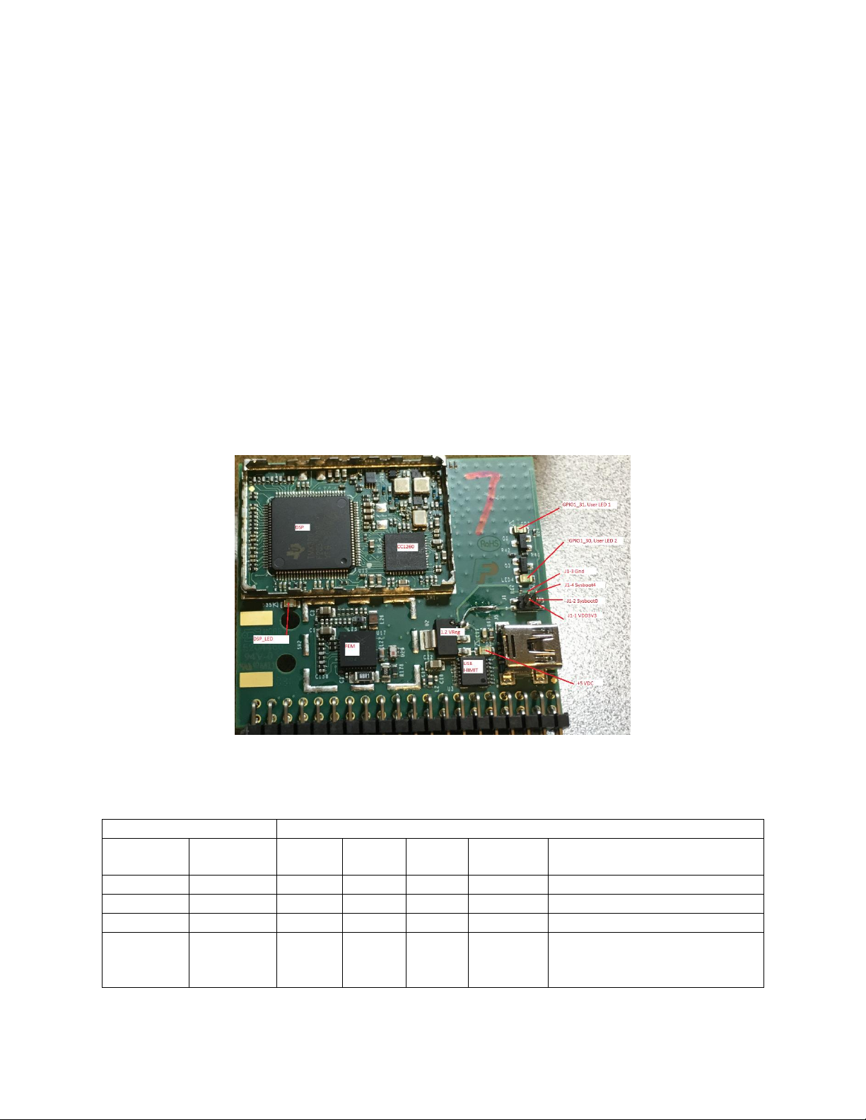
For Reference Only, Printed: 3/6/2018
Page 26 of 49
Expansion Connector Pinout
J4
PIN
LGA
Pin
Ball
ZCZ
Rail
LGA Name
MODES
34 140
H16
3.3
SPI1_SCLK
Test with SPITest1.exe
And Microchip SPI test
board.
See test section later in
this document.
(0) GMII1_COL
(1) RMII2_REFCLK
(2) SPI1_SCLK
(3) UART5_RXD
(4) MCASP1_AXR2
(5) MMC2_DAT3
(6) MCASP0_AXR2
(7) GPIO3_0
35
F15
3.3
UART0_RX
This is console so no other
testing required.
Linux Console Access
36 154
D16
3.3
GPIO1_17
Test with:
./gpio1_19.sh
(0) GPMC_A1
(1) GMII2_RXDV
(2) RGMII2_RCTL
(3) MMC2_DAT0
(4) GPMC_A17
(5) PR1_MII1_TXD3
(6) EHRPWM0_SYNCO
(7) GPIO1_17
37
3V3_EXP
Test with Meter or Scope
3V3_EXP
38 153
U14
3.3
GPIO1_18
Test with:
./gpio1_18.sh
(0) GPMC_A2
(1) GMII2_TXD3
(2) RGMII2_TD3
(3) MMC_DAT1
(4) GPMC_A18
(5) PR1_MII_TXD2
(6) EHRPWM1A
(7) GPIO1_18
39 Ground
40 Ground
P4 PIN DESCRIPTIONS
This section describes the pins on P8 that are not connected directly to the A8 processor. For those
connected directly to the A8 processor please refer to the TI AM33xA8ProductPreview document for
details of pin usage. Note that the Linux Device table will specify which pin peripheral is used for each
pin at power up.
P4-1 AND 2 +5.0 VDC
See the earlier section called “Itron Riva Dev Mini Power Supply Handling”
P4-18 HV_CMP
This pin is an input to the PMIC power supply chip on the iSOM module. Its purpose is to notify the
iSOM that power is failing and that it needs to shut down all of its power supply rails as fast as
possible. This is not a graceful shutdown.
A default voltage divider (100k and 28k resistors) holds this pin above 1VDC until the +5VDC supply
drops below 4.6 VDC. If it goes below 1 VDC it will cause a non-graceful shutdown. This input can be
driven below 1 VDC by user circuitry if a forced shutdown is required.
Page 27

Riva Edge Mini HW Design and User Guide Rev 1.01
ITRON PROPRIETARY & CONFIDENTIAL INFORMATION
For Reference Only, Printed: 3/6/2018
Page 27 of 49
There is another pin called EPF_IN* that provides a way of letting the system know of an Early Power
Fail condition to permit a graceful shutdown in hardware. Typically, enough capacitance would be
provided on the main (+5V) power supply line to allow the system to run long enough for the power
rails to be cycled down in the appropriate order with the appropriate delays before the HV_CPM
signal is applied through this pin. This signal is an over-ride of the EPF process.
P4-20 EPF_IN* (THIS SECTION REQUIRES WORK)
EPF* is the Early Power Fail input and is an active low. In other words, when EPF* is high there is no
presence of a power failure. EPF* is effectively an input to both the PIC and the A8. EPF* is mainly
used to allow the product motherboard to alert the module that power is about to be lost. It is
typically the first signal to go low when a shutdown is required.
EPF* can be provided to this pin or from circuitry on the board. The on-board circuitry will trigger
EPF* when the +5 VDC rail falls to 4.4 VDC. If you require another voltage, then R45 must be removed
from the board to use this pin.
EPF* is a required part of the power-on sequence and is required before the PIC will activate the
power rails for the A8. Therefor EPF* must be raised after, or simultaneously, when 5VDC is initially
applied. Typically, if there are hold-up capacitors on the main supply rail and EPF* is held low until
they are sufficiently charged to provide enough hold-up power for the system to shut down
gracefully.
If it is not high the PMIC will partially power the module (LDOs) but NOT power the A8 until it goes
high.
During normal operations this pin is used as part of the Early Power Fail system. PON_WAKEUP is
generated as a result of an EPF* signal and some timing delays.
EPF* (Early Power Fail) is created on the motherboard and sent to the module. It informs the A8 that
it must shut down as soon as possible. EPF* also goes to the communications module telling it that it
must send PON (Power Outage Notification) packets. After EPF* occurs the communications module
and the A8 are operating asynchronously with the A8s only job being to get shut down to conserve
power.
While the A8 is shutting down the communications module will put 3 timer values into the PIC via
the I2C bus. The communications module will also then enter a low power mode waiting for the PIC.
PON_WAKEUP is generated when the first timer expires in the PIC causing a PIC internal interrupt.
PON_WAKEUP is a normally low signal that is active high with a programmable high pulse. The
communications module sees PON_WAKEUP as an interrupt and exits low power mode to send a
message packet indicating that there has been a power loss.
Page 28

Riva Edge Mini HW Design and User Guide Rev 1.01
ITRON PROPRIETARY & CONFIDENTIAL INFORMATION
For Reference Only, Printed: 3/6/2018
Page 28 of 49
Once the PIC generates PON_WAKEUP the next timer value is loaded and the process is repeated a
total of three times. After the communications module has sent its three PON messages it then shuts
down.
P4-26 BATTERY
This is an input to the PCF8546A RTC chip. Its purpose is to provide a method of keeping the RTC
time accurate when there is no main power. The battery voltage can be between .9 and 5.0 VDC and
switchover thresholds can be set by software. Please see the PCF8563A RTC chip datasheet for
configuration and usage of this pin.
P4-37 3V3_EXP
See the previous section called “Itron Riva Dev Mini Power Supply Handling”
EXPANSION PERIPHERAL PORT USAGE
Multiple A8 peripherals are brought out on the Expansion Port. The following sections that help
explain their usage
SPI0
A8 name
CONN
Note
SPI0_CS1
NC
Dedicated to DSP
SPI0_CS0
J4-25
Dedicated to user
SPI0_MISO
J4-27
Shared by user and DSP
SPI0_MOSI
J4-29
Shared by user and DSP
SPI0_CLK
J4-31
Shared by user and DSP
SPI1
A8 name
CONN
Note
SPI1_CS1
NC
Dedicated to DSP
SPI1_CS0
J4-28
Dedicated to user
SPI1_MISO
J4-30
Shared by user and DSP
SPI1_MOSI
J4-32
Shared by user and DSP
SPI1_CLK
J4-34
Shared by user and DSP
AIN0...AIN3
A8 name
CONN
Note
AIN0
J4-11
Dedicated to user
AIN1
J4-13
Dedicated to user
AIN2
J4-14
Dedicated to user
AIN3
J4-16
Dedicated to user
Page 29

Riva Edge Mini HW Design and User Guide Rev 1.01
ITRON PROPRIETARY & CONFIDENTIAL INFORMATION
For Reference Only, Printed: 3/6/2018
Page 29 of 49
I2C2
Note that I2C2 requires a pull-up resistor to 3.3V on both SCL and SDA. The value should be around
2.2k but can vary depending on the devices you have connected.
A8 name
CONN
Note
AIN0
J4-15
Dedicated to user
AIN1
J4-17
Dedicated to user
DSP TO A8 INTERCONNECTS
This section describes the basic connection between the A8 processor and the RF DSP.
More needs to be added here.
A8 name
iSOM Pin
P8 CONN
RF Desc
DSP Name
DSP Pin
UART4_TX
175
P8-5
UART4_TX
SCI_DSP_RXDC
97
UART4_RX
190
P8-6
UART4_RX
SCI_DSP_TXDC
96
UART1_TX
71
P8-33
UART1_TX
SCI_DSP_RXDA
74
UART1_RX
57
P8-34
UART1_RX
SCI_DSP_TXDA
73
Page 30
Riva Edge Mini HW Design and User Guide Rev 1.01
ITRON PROPRIETARY & CONFIDENTIAL INFORMATION
For Reference Only, Printed: 3/6/2018
Page 30 of 49
RF CONNECTOR AND CABLE
There is a very small UF.L connector located between the DSP shield and J4 the expansion interface
connector. This is the connection for the radio transceiver. This mates with A HIROSE U.FL connector.
This device must be professionally installed.
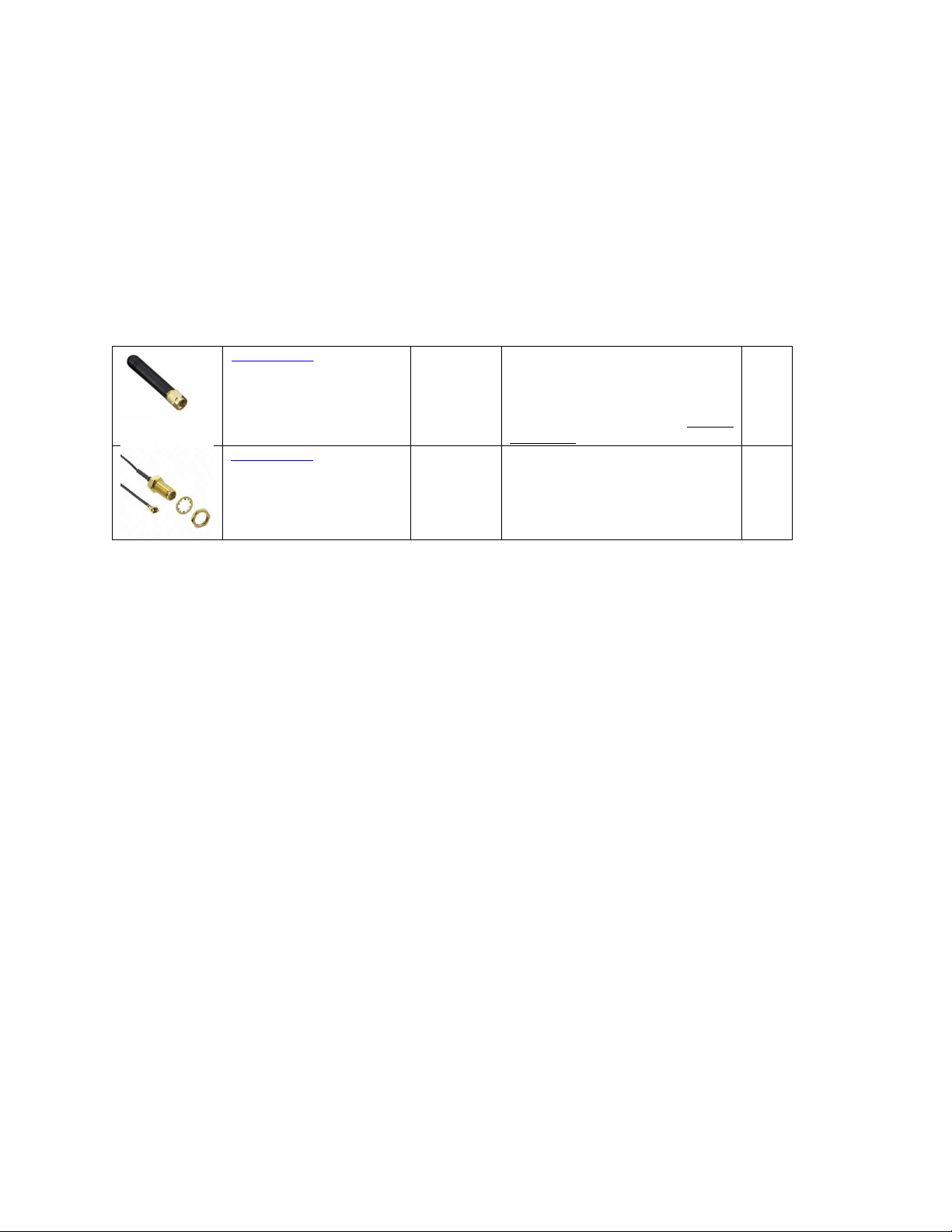
Only the following antennas are permitted or antennas of the same type but less peak gain.
Only specified antennas listed in this document may be used for integration of the OEM module to
comply with FCC emission limits! Please refer to the antenna tables in this document. Antenna and
RF Cable type and purchasing information are provided later in the document.
931-1040-ND
850MHz, 900MHz, 1.8GHz, 1.9GHz,
2.1GHz CDMA, DCS, EDGE, GPRS, GSM,
HSPA, PCS, UMTS, WCDMA Whip,
Straight RF Antenna 824MHz ~
960MHz, 1.71GHz ~ 2.17GHz 1.91dBi
@ 900MHz, SMA Male Connector
931-1186-ND
Cable Assembly Coaxial SMA to U.FL
Female to Female 1.13mm OD Coaxial
Cable 7.874" (200.00mm)
ATT@<2GHz = < 2.8dB/m
ATT < 0.56 dB
Page 31

Riva Edge Mini HW Design and User Guide Rev 1.01
ITRON PROPRIETARY & CONFIDENTIAL INFORMATION
For Reference Only, Printed: 3/6/2018
Page 31 of 49
DOWNLOADING, IF NECESSARY (LINUX)
The board firmware, and Linux in general, is made up of several images broken into multiple files.
Each file performs a different set of operations at different times. For details of what each file contains
please see a Linux Reference.
You will need the following files:
u-boot-spl.bin
u-boot.bin
MLO
u-boot.img
uImage
For the descriptions below it is assumed that the images are in a folder named images at the root of
your Linux system on your PC. It is also assumed your terminal is connected on /dev/ttyUSB0.
Enter a terminal program such as minicom. Connect to the main terminal port (UART0 by default) at
115800, N-8-1. Power on the board and it will begin outputting a continuous stream of “C” characters
at about 1-2 second intervals if it is an erased board or has the jumpers set as described in an earlier
section,
C:\Users\jbean\Documents\ItronProducts\CTO Design
Kit\LinuxTestApps\LinuxStuff\TestBuilds\register_hwtest_isom.config_images\bootloader
Wait until you see the “CCC” pattern and then exit the terminal. Now we put small version of u-boot
in RAM that can be used to FLASH the rest of the firmware. On the Linux host command line execute
the following:
sx -k /images/u-boot-spl.bin > /dev/ttyUSB0 < /dev/ttyUSB0
sx -k /images/u-boot.bin > /dev/ttyUSB0 < /dev/ttyUSB0
Once these programs complete re-enter the terminal application with the same settings as before.
Now you are executing the RAM version of u-boot and we can FLASH the rest of the code.
Run loady of MLO (ymodem)
When it completes do the following two commands:
nand erase 0x0 0x20000
nand write.i 0x82000000 0x0 0x20000
Run loady of u-boot.img (ymodem)
When it completes do the following two commands:
nand erase 0x80000 0x60000
nand write.i 0x82000000 0x80000 0x60000
Run loady of uImage (note may take 10 minutes or more depending on kernel size)
When it completes do the following two commands:
nand erase 0x5A0000 0xCE0000
nand write.i 0x82000000 0x5A0000 0xCE0000
Page 32

Riva Edge Mini HW Design and User Guide Rev 1.01
ITRON PROPRIETARY & CONFIDENTIAL INFORMATION
For Reference Only, Printed: 3/6/2018
Page 32 of 49
All of the code is now Flashed and ready to run. We need to reboot from the new FLASH image. Cycling
power works better but corrupts the RTC when there is no battery. So you may run bootm instead as
follows:
bootm ${loadaddr}
The system should now reboot from the FLASH image. Depending on the image you loaded you may
be given a chance to break the boot process when u-boot completes before getting into Linux.
ERASING FLASH IMAGE
If you need to erase the chip totally killing Linux and u-boot it can be done from u-boot or Linux.
ERASING FLASH IMAGE FROM U-BOOT
From the command line type:
nand erase.chip
ERASING FLASH IMAGE FROM LINUX
From the command line type:
flash_erase /dev/mtd4 0 0
And then:
flash_erase /dev/mtd8 0 0
Page 33

Riva Edge Mini HW Design and User Guide Rev 1.01
ITRON PROPRIETARY & CONFIDENTIAL INFORMATION
For Reference Only, Printed: 3/6/2018
Page 33 of 49
ITRON RIVA DEV MINI TEST PROCEDURE
This section of the document explains how to perform a basic hardware test on the Riva Edge Mini
using a test fixture, a solderless breadboard adapter or point-to-point wiring.
The tests are described as single item step-by-step actions allowing testing of a single piece of
hardware. For instance, if you are not sure a GPIO is working look up its test below and run its
respective test.
EQUIPMENT REQUIRED:
1. Itron Riva Dev Mini
2. Test Fixture (Optional)
3. Solderless Breadboard Adapter
4. Bench Power Supply capable of 5 VDC at 1.5 AMPs or greater with Ammeter
5. USB-To-Serial adapter cable with 4-pin connector or individual pins
a. 3.3 VDC Powered
b. Self Powered
i. Leave Pin 3.3 VDC pin disconnected
6. Oscilloscope or logic analyzer or at a minimum a logic probe.
7
7. Multi-meter
MINIMAL OPERATIONAL CONNECTIONS
This section describes how to connect power for each type of fixture or adapter. It also includes
connecting UART0. With these minimal connections you can operate the Linux system from a
terminal as console.
Note when making these connections power should be removed from the system.
We will describe all tests as though you are using a solderless breadboard adapter. Although a little
more complicated than using the test fixture is more likely that a user will have it. There is a
document that describes the test fixture usage on the google drive.
MINI DK TEST FIXTURE
1. Clamp Mini DK onto Test Fixture using spring clamps
2. Ensure that proper pins are inserted in test fixture for
a. +5 VDC to J4 Pin 1
b. Ground to J4 Pin 40
c. RX Pin to J4 Pin 33
d. TX Pin to J4 Pin 35
e. 3.3 VDC Input Pin to J4 Pin 37
i. If this USB-To-Serial adapter creates an output voltage do not connect this pin
7
Running the test scripts produces slow toggling signals for GPIO pins. Other pins such as I2C and SPI use much
faster signals that may require a scope.
Page 34

Riva Edge Mini HW Design and User Guide Rev 1.01
ITRON PROPRIETARY & CONFIDENTIAL INFORMATION
For Reference Only, Printed: 3/6/2018
Page 34 of 49
f. Ground Pin to J4 Pin 39
MINI DK SOLDERLESS BREADBOARD ADAPTER
1. Plug Mini DK into Solderless breadboard adapter if available
2. Connect +5 VDC Barrel connector, +5 on center contact, collar is ground.
3. Plug USB-To-Serial adapter into white connector
MINI DK DIRECT WIRING
This sections assumes you don’t have a fixture or solderless breadboard adapter. It assumes you are
using wires soldered to board or connector, push terminals on pins or mini jumper clips.
1. Connect +5 VDC to J4 Pin 1
2. Connect Ground to J4 Pin 40
3. Connect USB-To-Serial adapter as follows
a. RX Pin to J4 Pin 33
b. TX Pin to J4 Pin 35
c. 3.3 VDC Input Pin to J4 Pin 37
i. If this USB-To-Serial adapter creates an output voltage do not connect this pin
d. Ground Pin to J4 Pin 39
Page 35

Riva Edge Mini HW Design and User Guide Rev 1.01
ITRON PROPRIETARY & CONFIDENTIAL INFORMATION
For Reference Only, Printed: 3/6/2018
Page 35 of 49
SMOKE/BOOT TEST
1. Perform a visual inspection
a. Watch for shorts, solder blobs or other manufacturing issues
2. Make sure Power Supply is turned off
3. Connect Power Supply and UART as described above
4. Establish a terminal session at 115200, N, 8, 1
5. Prepare to monitor Ammeter
a. If exceeds 200ma immediately remove power
6. Turn on Power
8
a. If exceeds 500ma immediately remove power
b. If about 260ma the iSOM (A8) is programmed but DSP isn’t.
c. If about 460ma the iSOM (A8) and DSP are programmed.
7. Watch Terminal for data from Itron Riva Dev Mini
a. If “cccc”, repeating “c”s, then the board is minimally operational as far as hardware
but requires loading of MLO and u-boot and kernel if a kernel is required.
b. If u-boot starts but ends at a u-boot prompt without launching kernel, then the board
is minimally operational as far as hardware but the board requires loading of kernel
if a kernel is required.
c. If Linux Kernel starts and ends with a prompt the board is operational as far as the
Linux System.9
8. Proceed to specific hardware tests described below as needed. All scripts are located at on
the google drive.
8
Note the currents specified are for Board Revision 2 and may be different for other revisions. It is also possible
that there will be variances board to board depending on software revisions.
9
In this case you can tell if the DSP is programmed and running by looking at the total current draw on the
system. But that does not tell you it is capable of transmitting or receiving.
Page 36

Riva Edge Mini HW Design and User Guide Rev 1.01
ITRON PROPRIETARY & CONFIDENTIAL INFORMATION
For Reference Only, Printed: 3/6/2018
Page 36 of 49
LED TESTING
A script has been written to toggle each user LED that is located on the Mini DK board and they can
be visually monitored for activity.
The scripts are toggleamberled6.sh and toggleamberled6.sh.
GPIO TESTING
All GPIO pins can be tested in a similar fashion. A script is available to toggle each pin requiring you
to use an oscilloscope, logic probe or meter to monitor the pins. It will be necessary to substitute the
proper GPIO name when running the test script.
This test covers the following pins:
1. J4 Pin 3 GPIO3_18 (gpio3_18.sh)
2. J4 Pin 5 GPIO3_19 (gpio3_19.sh)
3. J4 Pin 7 GPIO3_20 (gpio3_20.sh)
4. J4 Pin 9 GPIO0_20 (gpio0_20.sh)
5. J4 Pin 19 GPIO3_21 (gpio3_21.sh)
6. J4 Pin 21 GPIO3_4 (gpio3_4.sh)
7. J4 Pin 23 GPIO3_0 (gpio3_0.sh)
8. J4 Pin 36 GPIO1_17 (gpio1_17.sh)
9. J4 Pin38 GPIO1_18 (gpio1_18.sh)
10. J4 Pin 22 GPIO1_20 (gpio1_20.sh)
11. J4 Pin 24 GPIO1_19 (gpio1_19.sh)
ANALOG INPUT PINS
This test covers testing the Analog input pins. There is a script available for testing each ADC. The
script will continuously read the ADC and display its value in hex on the screen. An adjustable power
supply can be used to apply power on the individual pins and varied to change the value being
displayed on the screen.
DO NOT EXCEED 1.8 VDC OR THE ADC WILL BE DAMAGED
This test covers the following four pins:
1. J4 Pin 11 AIN_0 (ad0.sh)
2. J4 Pin 13 AIN_1 (ad1.sh)
3. J4 Pin 14 AIN_2 (ad2.sh)
4. J4 Pin 16 AIN_3 (ad3.sh)
Page 37

Riva Edge Mini HW Design and User Guide Rev 1.01
ITRON PROPRIETARY & CONFIDENTIAL INFORMATION
For Reference Only, Printed: 3/6/2018
Page 37 of 49
I2C2 TESTING
Note that requires a pull-up resistor to 3.3V on both SCL and SDA. The value should be around 2.2k
but can vary depending on the devices you have connected.
This test covers testing the I2C port. We use the Linux i2ctools to do the basic test. This test covers
the following two pins:
1. J4 Pin 15 I2C2_SCL
2. J4 Pin 17 I2C2_SDA
Following is the actual command sent to the I2C port and the response from the Mini DK with no I2C
peripherals on I2C bus 2.
# /usr/sbin/i2cdetect -y -r 2
0 1 2 3 4 5 6 7 8 9 a b c d e f
00: -- -- -- -- -- -- -- -- -- -- -- -- -10: -- -- -- -- -- -- -- -- -- -- -- -- -- -- -- -20: -- -- -- -- -- -- -- -- -- -- -- -- -- -- -- -30: -- -- -- -- -- -- -- -- -- -- -- -- -- -- -- -40: -- -- -- -- -- -- -- -- -- -- -- -- -- -- -- -50: -- -- -- -- -- -- -- -- -- -- -- -- -- -- -- -60: -- -- -- -- -- -- -- -- -- -- -- -- -- -- -- -70: -- -- -- -- -- -- -- --
Now the same command with a Microchip PICKit I2C Demo board attached.
# /usr/sbin/i2cdetect -y -r 2
0 1 2 3 4 5 6 7 8 9 a b c d e f
00: -- -- -- -- -- -- -- -- -- -- -- -- -10: -- -- -- -- -- -- -- -- -- -- -- -- -- -- -- -20: 20 -- -- -- -- -- -- -- -- -- -- -- -- -- -- -30: -- -- -- -- -- -- -- -- -- -- -- -- -- -- -- -40: -- -- -- -- -- -- -- -- 48 49 -- -- -- 4d -- -50: 50 51 52 53 54 55 56 57 -- -- -- -- -- -- -- -60: -- -- -- -- -- -- -- -- -- -- -- -- -- -- -- -70: -- -- -- -- -- -- -- --
The following table shows the parts on the Demo Board and their respective device addresses. Note
that the datasheet shows the left shifted address assuming a r/w bit is inserted at bit 0. I2Cdetect
displays the Unshifted address without the r/w bit.
Part #
Description
Unshifted
Address
Shifted
Address
24LC02B
2Kbit Serial EEPROM
0xAx
0x5x
PKSERIAL-I2C1-ND
24LC02B, MCP9800, MCP3221,
TC1321, MCP23008 - Interface, I2C
Devices, 5 Evaluation Board
Page 38

Riva Edge Mini HW Design and User Guide Rev 1.01
ITRON PROPRIETARY & CONFIDENTIAL INFORMATION
For Reference Only, Printed: 3/6/2018
Page 38 of 49
MCP3221
Low-Power 12-Bit A/D Converter
0x9A
0x4D
TC1321
10-Bit Digital-to-Analog
Converter
0x90
0x48
MCP23008
8-Bit I/O Expander
0x40
0x20
MCP9801
High-Accuracy Temperature
Sensor
0x92
0x49
Page 39

Riva Edge Mini HW Design and User Guide Rev 1.01
ITRON PROPRIETARY & CONFIDENTIAL INFORMATION
For Reference Only, Printed: 3/6/2018
Page 39 of 49
SPI TESTING
This test covers testing the two SPI ports. All four pins are tested simultaneously by running a test
application individually for each port. The test application is called spitest0.exe for SPI0 and
spitest1.exe for SPI1.
A Microchip PICKit Serial SPI Demo Board is used for testing but a scope could be connected to the
SPI lines to watch activity. On the SPI Demo Board JP-7 and JP-8 must be installed. The test code will
change the LEDs located on the end of the board to show activity.
This test covers the following four pins: (spitest0.exe)
1. J4 Pin 25 SPIO0_CS0
2. J4 Pin 27 SPIO0_MISO
3. J4 Pin 29 SPIO0_MOSI
4. J4 Pin 31 SPIO0_SCLK
This test covers the following four pins: (spitest1.exe)
1. J4 Pin 28 SPI1_CSO
2. J4 Pin 30 SPI1_MISO
3. J4 Pin 32 SPI1_MOSI
4. J4 Pin 34 SPI1_SCLK
PKSERIAL-SPI1-ND
PICkit™ 1 - Interface, SPI Devices, 7
Evaluation Board
Page 40

Riva Edge Mini HW Design and User Guide Rev 1.01
ITRON PROPRIETARY & CONFIDENTIAL INFORMATION
For Reference Only, Printed: 3/6/2018
Page 40 of 49
UART0 TESTING
UART0 is the default UART for the console. So no specific testing is required since this UART is the
primary console.
1. J4 Pin 33 UART0_TX
2. J4 Pin 35 UART0_RX
USB1 TESTING
This test covers the testing of USB1.
1. J4 Pin 4 USB1_VBUS
2. J4 Pin 6 USB1_ID
3. J4 Pin 8 USB1_DRVVBUS
4. J4 Pin 10 USB1_DM
5. J4 Pin 12 USB1_DP
EPF* TESTING
To test this pin simply ground it for 5 seconds. When released from ground the system will restart
with a reset.
1. J4 Pin 20 EPF_IN*
HV_CMP TESTING
A default voltage divider (2 100k resistors) holds this pin at about 2.5 Volts. If it goes below 1 VDC it
will cause a non-graceful shutdown. To test this pin simply ground it for 5 seconds. When released
from ground the system will restart with a reset.
1. J4 Pin 18 HV_CMP
BATTERY PIN TESTING
The following pins do not have tests defined at this time.
2. J4 Pin 26 BATTERY
Page 41

Riva Edge Mini HW Design and User Guide Rev 1.01
ITRON PROPRIETARY & CONFIDENTIAL INFORMATION
For Reference Only, Printed: 3/6/2018
Page 41 of 49
Page 42

Riva Edge Mini HW Design and User Guide Rev 1.01
ITRON PROPRIETARY & CONFIDENTIAL INFORMATION
For Reference Only, Printed: 3/6/2018
Page 42 of 49
DSP PROGRAMMING (REQUIRES FIXTURE)
Programming the DSP requires a programming fixture and a XDS 200 JTAG programmer and a
Windows application called CCS UniFlash 3.1.0.10
First place the EUT on the fixture and connect the JTAG to the fixture following the instructions from
the fixture user guide. Connect the JTAG USB cable to the PC also. Power on the fixture.
Note this programming can be done while the iSOM programming script is running.
Launch the CCS UniFlash application and you should see the following window.
Go to File::Open Existing Target Configuration and use the dialog to browse to wherever you put the
ACTDongleUniFlashConfiguration.ccxml file. You will see a “Progress Information” dialog explaining
that it is starting.
After completing you should see:
10
There may be Linux support for this but I am not aware of it at this writing.
Page 43
Riva Edge Mini HW Design and User Guide Rev 1.01
ITRON PROPRIETARY & CONFIDENTIAL INFORMATION
For Reference Only, Printed: 3/6/2018
Page 43 of 49
On the left you are shown a summary of both DSP cores. Click on the black triangle that is next to
“Flash Settings” for each core to close that information. This step is optional.
Page 44

Riva Edge Mini HW Design and User Guide Rev 1.01
ITRON PROPRIETARY & CONFIDENTIAL INFORMATION
For Reference Only, Printed: 3/6/2018
Page 44 of 49
Now click on “Programs” for Core 1 (CPU1) to select the file for the first core. The ccxml file you
loaded already has the proper filename in place.
Now click on the “Program” soft-button on the right panel. You will see a “Progress Information”
dialog explaining the steps as it programs.
Now click on “Programs” for Core 2 (CPU2) to select the file for the first core. The ccxml file you
loaded already has the proper filename in place.
Now click on the “Program” soft-button on the right panel. You will see a “Progress Information”
dialog explaining the steps as it programs.
Both Cores are now programmed.
Page 45

Riva Edge Mini HW Design and User Guide Rev 1.01
ITRON PROPRIETARY & CONFIDENTIAL INFORMATION
For Reference Only, Printed: 3/6/2018
Page 45 of 49
USB-TO-SERIAL ADAPTERS
Since most PCs no longer have serial ports it is customary to use a USB-to-serial TTL converter cable.
We typically use cables made by FTDI (Future Technology Devices International LTD). It is possible
to use cables from other manufacturers that meet the same specifications. Use the datasheet for the
particular cable you have to identify the 4 required signals (Rx, Tx, Gnd, +3.3VDC In) along with
drawing below to connect your board.
We typically use a USB-to-Serial11 converter to bring UART0 out as our terminal port. This port
operates in 115kbps N81 format. The adapter is powered by 3.3VDC from the Itron Riva Dev Mini
board.
One cable is the TTL-232R-RPI from FTDI sold by Digi-Key as part number 768-1024-ND. This
cable has 3 wires with connectors designed to be individually placed on individual pins. Because
there are only 3 pins the 3.3 VDC supplies are not connected together.
Figure 8 - FTDI TTL-232R-RPI
Another cable is the TTL-232R-3V3-WE from FTDI sold by Digi-Key as part number 768-1016-ND.
This cable has 6 unterminated wires of which only 4 are used. The image below shows the two ends
of this cable using a 4-pin female connector.
11
Note this is a serial 0VDC to 3.3VDC connection NOT RS-232.
Page 46
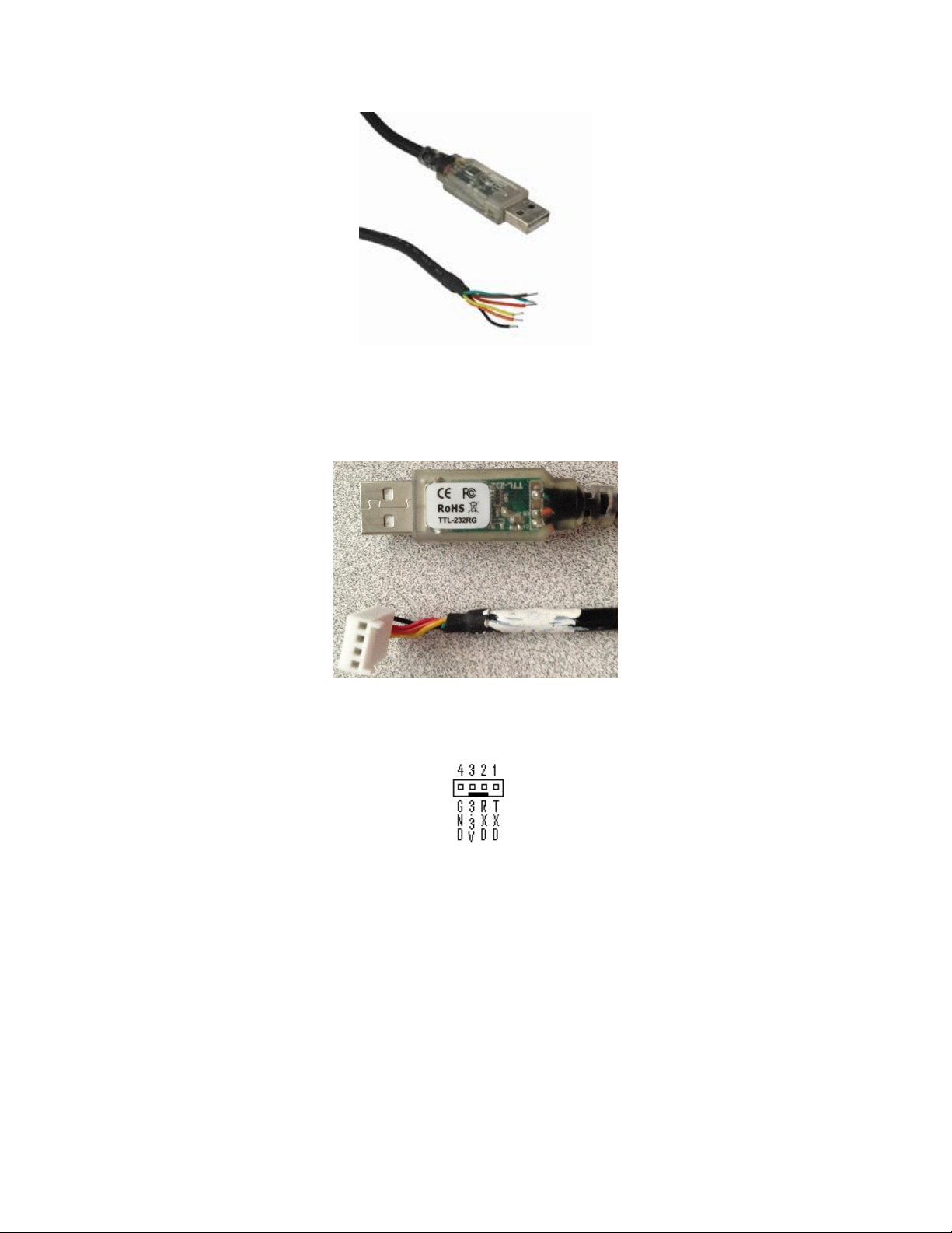
Riva Edge Mini HW Design and User Guide Rev 1.01
ITRON PROPRIETARY & CONFIDENTIAL INFORMATION
For Reference Only, Printed: 3/6/2018
Page 46 of 49
Figure 9 - FTDI TTL232R-3V3-WE
The white housing shown is a Molex part number –22013047 or Digi-Key WM2002-ND.
Each wire requires a female pin Molex part number – 0008500114 or Digi-Key WM1114-ND.
Figure 1: Serial-To-USB Adapter cable
Figure 2: Typical 4-Pin Keyed Adapter
Page 47

Riva Edge Mini HW Design and User Guide Rev 1.01
ITRON PROPRIETARY & CONFIDENTIAL INFORMATION
For Reference Only, Printed: 3/6/2018
Page 47 of 49
USB CABLES
The board can act as a USB host or a USB peripheral depending on the cable chosen. How the board
acts is determined by using one of the following cables select USB Host or USB peripheral.
To use the ACT board as an USB host the ACT board must be powered by the expansion connector +5
V pins. The white cable with a Mini-A to Type-A Receptacle would be used. The peripheral being
hosted, for instance a thumb drive, would be plugged into Type-Receptacle and Mini-A plug into the
Mini-AB Jack on the board.
To use the ACT board as a USB peripheral the board must be powered by the USB cable12. For this
mode the black cable with a Mini-B to Type-A Plug would be used. The Mini-B would plug into the
ACT board and the Type-A plug would plug into the PC or other host.
12
This may change. It may be possible to power the board by the expansion connector while it is serving as a
peripheral to allow more power.
AE1450-ND
Board looks like
USB Device, and is
powered by Host
USB 2.0 Cable A Male to Mini B Male 3.28'
(1.00m) Shielded
10-00003-ND
Board looks like
Host, and Powers
device
USB 2.0 Cable A Female to Mini A Male
0.33' (100.0mm) Shielded
Page 48

Riva Edge Mini HW Design and User Guide Rev 1.01
ITRON PROPRIETARY & CONFIDENTIAL INFORMATION
For Reference Only, Printed: 3/6/2018
Page 48 of 49
APPENDIX A: FCC RELATED STATEMENTS
DECLARATION OF CONFORMITY
The Itron Riva Dev Mini Module complies with Part 15 of the FCC rules and regulations. Compliance
with the labeling requirements, FCC notices and antenna usage guidelines is required. To fufill FCC
Certification, the OEM must comply with the following regulations:
1. The system integrator must ensure that the text on the external label provided with this
device is placed on the outside of the final product.
2. Itron Riva Dev Mini Module may only be used with antennas that have been tested and
approved for use with this module [refer to the antenna tables in this section].
OEM LABELING REQUIREMENTS
WARNING: The Original Equipment Manufacturer (OEM) must ensure that FCC labeling
requirements are met. This includes a clearly visible label on the outside of the final
product enclosure that displays the contents shown in the figure below. Required FCC
Label for OEM products containing the Itron Riva Dev Mini Module.
Contains FCC ID: 2ANHYMINI1
The enclosed device complies with Part 15 of the FCC Rules. Operation is subject to the following two
conditions: (i.) this device may not cause harmful interference and (ii.) this device must accept any
interference received, including interference that may cause undesired operation.
FCC NOTICES
IMPORTANT: The Itron Riva Dev Mini Module has been certified by the FCC for use with other
products without any further certification (as per FCC section 2.1091). Modifications not expressly
approved by Itron, Inc. could void the user's authority to operate the equipment.
OEMs must test final product to comply with unintentional radiators (FCC section 15.107 & 15.109)
before declaring compliance of their final product to Part 15 of the FCC Rules.
The RF module has been certified for remote and base radio applications. If the module will be used
for portable applications, the device must undergo SAR testing.
This equipment has been tested and found to comply with the limits for a Class B digital device,
pursuant to Part 15 of the FCC Rules. These limits are designed to provide reasonable protection
against harmful interference in a residential installation. This equipment generates, uses and can
radiate radio frequency energy and, if not installed and used in accordance with the instructions, may
cause harmful interference to radio communications. However, there is no guarantee that
interference will not occur in a particular installation.
If this equipment does cause harmful interference to radio or television reception, which can be
determined by turning the equipment off and on, the user is encouraged to try to correct the
interference by one or more of the following measures: Re-orient or relocate the receiving antenna,
Increase the separation between the equipment and receiver, connect equipment and receiver to
outlets on different circuits, or Consult the dealer or an experienced radio/TV technician for help.
Page 49

Riva Edge Mini HW Design and User Guide Rev 1.01
ITRON PROPRIETARY & CONFIDENTIAL INFORMATION
For Reference Only, Printed: 3/6/2018
Page 49 of 49
RF EXPOSURE
This equipment complies with FCC radiation exposure limits set forth for an uncontrolled
environment. This equipment should be installed and operated with minimum distance 20cm
between the radiator and your body. This transmitter must not be co-located or operating in
conjunction with any other antenna or transmitter.
FCC-APPROVED ANTENNAS (902-928 MHZ)
The Itron Riva Dev Mini Module can be installed utilizing antennas and cables constructed with
standard connectors (Type-N, SMA, TNC, etc.) if the installation is performed professionally and
according to FCC guidelines. For installations not performed by a professional, non-standard
connectors (RPSMA, RPTNC, etc.) must be used.
The Itron Riva Dev Mini Module have been tested and approved for use with all the antennas listed
in the tables below.
Antennas not listed in the table must be tested to comply with FCC Section 15.203 (Unique Antenna
Connectors) and Section 15.247 (Emissions).
OMNI-DIRECTIONAL ANTENNAS
Manufacturer
Part Number
Type
Peak Gain
@ 902-928MHz
Min. cable loss
@ 902-928MHz13
Taoglas Limited
TG.22.0111
Monopole
1.91 dBi
0.56 dB
13
The cable used was for FCC certification was 200mm Taoglas CAB.718, with attenuation of 2.8 dB/m below
2 GHz.
 Loading...