

Page 1
Hardware
Integrator's Guide
CreataLink™ 2XT
ReFLEX 25 and 50 Technologies
Page 2

Page 3

CreataLink2 XT Hardware Integrator’s Guide Foreword
91B
1Foreword
1Foreword
Foreword
Foreword
Customer Information
The information in this manual has been reviewed for accuracy. However, no
responsibility is assumed for inaccuracies. SmartSynch, Inc., reserves the right to
make changes to any products discussed h erein. The inf ormation in th is document
is subject to change without notice. SmartSynch, Inc. assumes no liability for
hardware or software damage or loss of data due to errors or omissions in this
manual. SmartSynch, Inc. does not assume any liability arising from the application
or use of any products or circuits described here in. Neither do es SmartSynch, Inc.
convey any license under its patents or right of others.
For technical support and questi ons concerning the Creat aLink2 XT and documentation, refer to our web site at www.smartsynch.com.
Computer Software Copyrights
The SmartSynch products described in this manual include copyrighted SmartSynch computer software stored in semiconductor memories and other media . Laws
in the United States and other countries preserve for SmartSynch, Inc. certain
exclusive rights for copyrighted computer programs, including the exclusive right
to copy or reproduce in any form the copyrighted computer software.
Trademarks
Accordingly, any copyrighted SmartSynch computer software contained in the
SmartSynch products described in this manual cannot be copied or reproduced in
any manner without the express written permission of SmartSynch, Inc..
Furthermore, the purchase of SmartSynch products doe s not grant, either directly
or by implication, estoppel, or otherwise, any license under the copyrights, patents
or patent applications of SmartSynch, Inc., except for the normal, non-exclusive,
royalty-free license to use that arises by operation of law in the sale of a product.
Portions of the software described in this manual are copyrighted by Motorola, Inc.
CreataLink®2 XT is a registered trademark of Sma rtSynch, Inc.
Motorola, the stylized M logo, CLP™, FLEX™, FLEXsuite™, and ReFLEX™ are
trademarks or registered trademarks of Motorola, Inc.
Microsoft®, Windows®, and Windows NT® are registered trademarks of Micro soft
Corporation.
Solaris™ is a trademark of Sun Microsystems Inc.
UNIX® is a registered trademark of X/Open Compan y Ltd.
July 23, 2002 1-1
Page 4

Foreword CreataLink2 XT Hardware Integrator’s Guide
Important Safety Information
Important Safety Information
The installation, maintenance, and/or operation of this equipment could present
potentially unsafe conditions , including, but not limited to, electr ical shock, improp
er voltage to components. Improper o peration could cause personal injury, death or
damage to property.
Read Instructions
Read all safety instructions before you operate the Data Transceiver or maintenance equipment. Retain these safety instructions for future reference. Specialized
procedures and instructions are required and must be followed. All applicable safety
procedures, such as Occupational, Safety, and Health Administration (OSHA)
requirements, Nation al Elect ric Cod e Require ments, local code req uirements, safe
working practices and good judgement must be used by personnel.
Heed Admonitions
Adhere to all warnings on the equipment and in the operating instructions. Follow
all operating and usag e instructions. The follow ing two safety admonitions are used
in this manual:
-
Caution: Emphasizes information about actions which could result in
G
E
equipment damage.
Warning: Emphasizes information about actions which could result in
personal injury.
Mounting
Mount the equipment only as recommended by the manufacturer. Situate the
equipment away from heat sources such as radiators, heat registers, stoves, or other
equipment (including amplifiers) that produces heat.
Power Sources and Grounding
Connect the equipment to the type of power source described in the installation
instructions, or as marked on the equipment. Do not defeat the grounding or
polarization provisions of the equipment. Turn the circuit b reaker off when equip
ment is to be left unused for long periods of time.
-
1-2 July 23, 2002
Page 5

CreataLink2 XT Hardware Integrator’s Guide Foreword
Important Safety Information
Damage Requiring Service
Do not attempt to perform service functions that are not described in the operating
instructions. Refer all such servicing to qualified service personnel.
Motorola, Inc. is not responsi ble for static damag e to equipment not sold under the
Motorola logo.
FCC Compliance Statement
This product generates, uses and can radiate radio frequency (RF). If it is not
installed and used in accordance with the instruction manual, it can cause harmful
interference to radio communications. It has been tested and c omplies with the
limits for a Class B digital device, pursuant to Part 15 of the Federal Communica
tions Commission (FCC) code of federal regulations, which are designed to provide
reasonable protection against harmful interference in a residential installation.
However, there is no guarantee that interference will not occur in a particular
installation. If this equipment causes harmful interference to radio or television
reception, the user should try and correct the interference by one or more of the
following measures:
Reorient or relocate the receiving/transmitting antenna.
-
Increase the separation between the equipment and the CreataLink2 XT device.
Connect the equipment into an outlet on a circuit di ff erent from t hat to which t he
CreataLink2 XT device is connected.
Interference must be corrected at the user’s expense. Consult the dealer or an
experienced radio/TV technician for help.
July 23, 2002 1-3
Page 6

Foreword CreataLink2 XT Hardware Integrator’s Guide
Important Safety Information
1-4 July 23, 2002
Page 7

GENERAL
Page 8

Page 9

CreataLink2 XT Hardware Integrator’s Guide General
91B
2General
Contents
Contents
About this Document . . . . . . . . . . . . . . . . . . . . . . . . . . . . . . . . . . . . . . . . . . . . . . . . . . . . . . . . . . . . . . . . . . . . . . . . . . . . . . .2-1
Audience . . . . . . . . . . . . . . . . . . . . . . . . . . . . . . . . . . . . . . . . . . . . . . . . . . . . . . . . . . . . . . . . . . . . . . . . . . . . . . . . . . .2-1
Conventions . . . . . . . . . . . . . . . . . . . . . . . . . . . . . . . . . . . . . . . . . . . . . . . . . . . . . . . . . . . . . . . . . . . . . . . . . . . . . . . .2-1
Related Publications . . . . . . . . . . . . . . . . . . . . . . . . . . . . . . . . . . . . . . . . . . . . . . . . . . . . . . . . . . . . . . . . . . . . . . . . . . . . . . . .2-2
Product Description . . . . . . . . . . . . . . . . . . . . . . . . . . . . . . . . . . . . . . . . . . . . . . . . . . . . . . . . . . . . . . . . . . . . . . . . . . . . . . . .2-3
Architecture . . . . . . . . . . . . . . . . . . . . . . . . . . . . . . . . . . . . . . . . . . . . . . . . . . . . . . . . . . . . . . . . . . . . . . . . . . . . . . . .2-4
Components . . . . . . . . . . . . . . . . . . . . . . . . . . . . . . . . . . . . . . . . . . . . . . . . . . . . . . . . . . . . . . . . . . . . . . . . . . . . . . . .2-4
Features . . . . . . . . . . . . . . . . . . . . . . . . . . . . . . . . . . . . . . . . . . . . . . . . . . . . . . . . . . . . . . . . . . . . . . . . . . . . . . . . . . . . . . . . . .2-5
Specifications . . . . . . . . . . . . . . . . . . . . . . . . . . . . . . . . . . . . . . . . . . . . . . . . . . . . . . . . . . . . . . . . . . . . . . . . . . . . . . . . . . . . .2-6
Environmental Constraints . . . . . . . . . . . . . . . . . . . . . . . . . . . . . . . . . . . . . . . . . . . . . . . . . . . . . . . . . . . . . . . . . . .2-7
Power Requirements . . . . . . . . . . . . . . . . . . . . . . . . . . . . . . . . . . . . . . . . . . . . . . . . . . . . . . . . . . . . . . . . . . . . . . . . .2-8
Connectors Description . . . . . . . . . . . . . . . . . . . . . . . . . . . . . . . . . . . . . . . . . . . . . . . . . . . . . . . . . . . . . . . . . . . . . .2-11
Accessories . . . . . . . . . . . . . . . . . . . . . . . . . . . . . . . . . . . . . . . . . . . . . . . . . . . . . . . . . . . . . . . . . . . . . . . . . . . . . . . .2-13
Typical Configurations . . . . . . . . . . . . . . . . . . . . . . . . . . . . . . . . . . . . . . . . . . . . . . . . . . . . . . . . . . . . . . . . . . . . . .2-14
Air Interface . . . . . . . . . . . . . . . . . . . . . . . . . . . . . . . . . . . . . . . . . . . . . . . . . . . . . . . . . . . . . . . . . . . . . . . . . . . . . . . . . . . . . .2-16
Air Interface Protocol . . . . . . . . . . . . . . . . . . . . . . . . . . . . . . . . . . . . . . . . . . . . . . . . . . . . . . . . . . . . . . . . . . . . . . .2-16
ReFLEX Network Operation . . . . . . . . . . . . . . . . . . . . . . . . . . . . . . . . . . . . . . . . . . . . . . . . . . . . . . . . . . . . . . . . . .2-17
Product Functionality . . . . . . . . . . . . . . . . . . . . . . . . . . . . . . . . . . . . . . . . . . . . . . . . . . . . . . . . . . . . . . . . . . . . . . . . . . . . . .2-18
Operating System . . . . . . . . . . . . . . . . . . . . . . . . . . . . . . . . . . . . . . . . . . . . . . . . . . . . . . . . . . . . . . . . . . . . . . . . . . 2 -18
Power-up Operating Mode . . . . . . . . . . . . . . . . . . . . . . . . . . . . . . . . . . . . . . . . . . . . . . . . . . . . . . . . . . . . . . . . . . .2-18
Message-Search Operating Mode . . . . . . . . . . . . . . . . . . . . . . . . . . . . . . . . . . . . . . . . . . . . . . . . . . . . . . . . . . . . . .2-18
Address Capability . . . . . . . . . . . . . . . . . . . . . . . . . . . . . . . . . . . . . . . . . . . . . . . . . . . . . . . . . . . . . . . . . . . . . . . . .2-19
Duplicate Message Detection . . . . . . . . . . . . . . . . . . . . . . . . . . . . . . . . . . . . . . . . . . . . . . . . . . . . . . . . . . . . . . . . .2-19
Message Deletion . . . . . . . . . . . . . . . . . . . . . . . . . . . . . . . . . . . . . . . . . . . . . . . . . . . . . . . . . . . . . . . . . . . . . . . . . . .2-19
Unit IDs . . . . . . . . . . . . . . . . . . . . . . . . . . . . . . . . . . . . . . . . . . . . . . . . . . . . . . . . . . . . . . . . . . . . . . . . . . . . . . . . . .2-19
Message Storage and Lengths . . . . . . . . . . . . . . . . . . . . . . . . . . . . . . . . . . . . . . . . . . . . . . . . . . . . . . . . . . . . . . . .2-20
Acknowledgment of Received Messages . . . . . . . . . . . . . . . . . . . . . . . . . . . . . . . . . . . . . . . . . . . . . . . . . . . . . . . . .2-21
Registration Request . . . . . . . . . . . . . . . . . . . . . . . . . . . . . . . . . . . . . . . . . . . . . . . . . . . . . . . . . . . . . . . . . . . . . . . .2-21
Configuration Parameters . . . . . . . . . . . . . . . . . . . . . . . . . . . . . . . . . . . . . . . . . . . . . . . . . . . . . . . . . . . . . . . . . . . .2-21
PPS Utility . . . . . . . . . . . . . . . . . . . . . . . . . . . . . . . . . . . . . . . . . . . . . . . . . . . . . . . . . . . . . . . . . . . . . . . . . . . . . . . .2-21
End-User Application Software . . . . . . . . . . . . . . . . . . . . . . . . . . . . . . . . . . . . . . . . . . . . . . . . . . . . . . . . . . . . . . . 2 -22
Serial Interface . . . . . . . . . . . . . . . . . . . . . . . . . . . . . . . . . . . . . . . . . . . . . . . . . . . . . . . . . . . . . . . . . . . . . . . . . . . .2-22
June 18, 2002 2-i
Page 10

General CreataLink2 XT Hardware Integrator’s Guide
Contents
2-ii June 18, 2002
Page 11

CreataLink2 XT Hardware Integrator’s Guide General
2General
About this Document
About this Document
This document summarizes the product features and describes how to install and
integrate the CreataL ink2 XT data transc eiver into an off-board a pplication. If you
are developing an on-board/embedded application, use the Software Integrator’s
Guide listed in the Related Publications Section in conjunction with this manual.
This document is organized in sections as follows:
• Section 1: Foreword - A brief introduction to this document, licensing information, safety guidelines, and a general description of the data transceiver.
• Section 2: General - Information about this document, references, installation
instructions, troubleshooting tips an d product features.
• Section 3: The Integration Overview - Integration (interface) overview.
• Section 4: Hardware Integration - The development environment, accessories,
and options.
• Section 5: Testing - installation, troubleshooting, and diagnostic mode.
• Section 6: Parts information - Part numbers and ordering information.
• Appendix A: Abbreviations and Acronyms
• Appendix B: Desense - A discussion of desense, EMI testing procedures, and
EMI control.
• Appendix C - FLEXsuite of Application Protocols - FLEX technology explained,
licensing information, and licensee form.
Audience
Conventions
This document was created for third-party developers who install the CreataLink2
XT data transceiver and deve lop app lication pro grams that co mmunicate wit h the
unit. Use of this manual to build applications for separate sale or license in
connection with data transceivers NOT purchased from SmartSynch, Inc. is unau
thorized and requires separate written permission from SmartSynch, Inc.
Special characters and typefaces, listed and described below, are used in this
publication to emphasize certain types of information.
Note: Emphasizes additional information pertinent to the subject matter.
➧
Caution: Emphasizes informa tion abo ut actio ns which may resu lt in equi pment
G
E
damage.
Warning: Emphasizes information about actions which may result in personal
injury.
Commands are shown like this
-
July 23, 2002 2-1
Page 12

General CreataLink2 XT Hardware Integrator’s Guide
Related Publications
Related Publications
The following documents provide additional information to integrators and application developers:
• Communication Linking Protocol Reference Manual,
publication 6881033B20
• CreataLink2
publication 6881033B45
• CreataLink2
publication 6881036B30
• Software Integrator’s Guide, publication 6881033B65
®
XT R50 Programming Software Guide - Integrators,
®
XT R25 Programming Software Guide,
2-2 July 23, 2002
Page 13
CreataLink2 XT Hardware Integrator’s Guide General
Product Description
Product Description
The CreataLink2 XT device is a two-way data transceiver that supports the
ReFLEX protocol. The CreataLink2 XT device can initiate transmissions into a
ReFLEX Narrow Band Personal Communications System (NBPCS) network, re
ceive and decode data, and store it. It can forward messages it receives from the
ReFLEX network to an interconnected hos t device via an RS-232 level or TransistorTransistor Logic (TTL) level serial port. The CreataLink2 XT device performs all
necessary ReFLEX protocol processing to maintain connection to the ReFLEX
network, accurately receives and acknowledges messages, and delivers messages
in conformance with protocol requirements.
The CreataLink2 XT provides an 8-bit, bi-directional parallel Input/Output (I/O)
port. Each bit can be configured individually as an input or output by the integrator
or end-user. The product also has two Analog-to-D igital (A/D) input ports for
customer use.
An additional pin is provi ded for a secondary battery so urce. This secondary source
can be used to back-up RAM contents in the event of a power failure and can be
selected through software to power the transmitter.
The CreataLink2 XT device can support an off-board application configuration (see
Figure 2-1 below). Off-board applications communicate with the CreataLink2 XT
using the Communications Linking Protocol (CLP).
-
Data collection
pt -machine,
meter, car, etc.
Discret e signals
Data collection
pt -machine,
meter, car, etc.
Discret e signals
CreataLink2 XT
Interface
Board for
proto col
translation
CLP
SERIAL
CLP
APP
I/O, A/D Port
SMA
Off-board host control over serial
port interface. Platform acts as
modem. Parallel I/ O and A/D port
control via host over serial link.
990441
Figure 2-1. Off-board Configuration
The CreataLink2 XT also supports an on-board application configuration which
enables third parties to write custom resident applications. This usually eliminates
the need for an external application board.
CreataLi nk2 XT
Custom Serial
Interface
SERIAL
3rd
PARTY
APP
I/O, A/D Port
SMA
On-board host operation via 3rd party
application.
990442
Figure 2-2. On-board Configuration
July 23, 2002 2-3
Page 14

General CreataLink2 XT Hardware Integrator’s Guide
Product Description
Architecture
The data transceiver’s software architecture is based upon the FLEX Kernel realtime operating system. With the addition of ReFLEX stack software, a message
manager, and the CLP default application, it provides a third-party embedded
messaging Application Programmer Interface (API). Ownership of the serial port
can be passed to a third-party application in place of the CLP application via an
application framework provided by SmartSynch, Inc. An ARM core based micropro
cessor provides the following features:
• 32-bit addressi ng
• 8, 16, and 32-bit data
• State-of-the-art softwar e development tools
• Industry standard Joint Test Action Group (JTAG) port
• Debugging support tools and environment via JTA G port
The serial port data interface supports the CLP application. The CLP serial
interface commands the data transceiver to obtain status information about the
network, transmit messages, and download received messages.
Components
-
The CreataLink2 XT hardware incorporates RF, digital, and analog circuitry on one
Printed Circuit Board (PCB). The product contains no housing and is sold as an
Original Equipment Manufacturer (OEM) product. The data transceiver has an
industry-standard Sub-Miniature connector (SMA) connection for cabling to a
remote antenna.
2-4 July 23, 2002
Page 15

CreataLink2 XT Hardware Integrator’s Guide General
Features
Features
The CreataLink2 XT device incorporates the following features.
• Compact package with four mounting holes
• External SMA female coaxial connector
• Configurable battery-save mode for reduced a verage power consumption
• Selectable transmi t power at antenna connector
NUF3902: 0.5W, 0.75W, 1.0W, 1.5W and 2.0W
NUF8006: 0.25W, 0.5W, 1.0W, 1.5W, and 2.0W
• Asynchronous transistor-transistor logic (TTL) or RS-232 serial port interface
that supports standard baud
• Alternate transmitter power source connection
• 8 Bi-directional I/O lines available for external interfacing; 2 driven outputs
and 6 open collectors
• 2 A/D input lines available for reading analog signals
• Receive frequency range:
NUF3902: 940-941 MHz
NUF8006: 929-941 MHz
• Transmit frequency range:
NUF3902: 901-902 MHz
NUF8006: 896-902 MHz
• Two-way paging protocols:
NUF3902: ReFLEX 50 (R50)
NUF8006: ReFLEX 25 (R25)
• Duplicate message detection/deletion
• Out-of-range indication
• Individual and broadcast message addressing
• 2000-byte uplink message length
• Single fragment, approximately 1000-byte downlink message length
• Backup battery option for SRAM
• FLASH for third-party on-board application or non-volatile st orage
•32KB RAM for messages
• JTAG interface for software debugging
•External reset
Although the data transceiver can receive messages of up to 1000 bytes in length,
➧
the carrier might not send this amount of data in a single transmission. Obtain
maximum single fragment message length from your carrier.
July 23, 2002 2-5
Page 16

General CreataLink2 XT Hardware Integrator’s Guide
Specifications
Specifications
T able 2-1. General Specifications
Item Specification Specification
Board Kit Number NUF3902 NUF8006
Coding format ReFLEX 50 ReFLEX 25
Serial Protocol CLP or third-party application CLP or third-party application
Operating temperature -40oC to +85oC -40oC to +85oC
22-pin vertical shroud ed header for combined
Interface
Power supply
requirements
Backup battery/
alternate transmit
power supply
requirements
Physical dimensions
Antenna Connector 50 Ohm SMA female connector 50 Ohm SMA female connector
Transm itter spec ific ation s:
Frequency 901–902 MHz 896-902 MHz
RF power output (at
antenna port)
power supply, serial , and p arallel I/O in terface.
8-pin vertical shrouded header for JTAG
interface; SMA connector for antenna
5-12 Vdc, 2.5A minimum, 100 mVpp ripple up
to 5 MHz (worst case estimate if sourcing/
sinking I/O at max values)
3-9 Vdc, 1 mA if used for RAM backup only.
5-9Vdc, 1.4A minimum, 10 0 mVpp ripple up to
5 MHz if used for transmitter supply (Battery
voltage must b e equal to or less t han the main
supply voltage)
Length: 3.75 in (95.25 mm) Length: 3.75 in (95.25 mm)
Width: 1.75 in (44.45 mm) Width: 1.75 in (44.45 mm)
Height: 0.7 in (17.78 mm) Height: 0.7 in (17.78 mm)
Weight: 1.5 oz. (42.5 grams) Weight: 1.5 oz. (42.5 grams)
0.5W, 0.75W, 1.0W, 1.5W, and 2.0W 0.25W, 0.5W, 1.0W, 1.5W, and 2.0W
22-pin vertical shrouded header for combined
power supply, serial, and parallel I/O interface.
8-pin vertical shrouded header for JTAG
interface; SMA connector for antenna
5-16 Vdc, 2.5A minimum, 100 mVpp ripple up
to 5 MHz (worst case estimate if sourcing/
sinking I/O at max values)
3-9 Vdc, 1 mA if used for RAM backup only.
5-9 Vdc, 1.4A minimum, 100 mVpp ripple u p to
5 MHz if used for transmitter supply (Battery
voltage must be equal to or less than the main
supply voltage)
Transmit data bit rate 9600 bits per second (bps) 800, 1600, 6400, 9600 bps
Modulation 4-level Frequency Shift Keying (FSK) 4-level FSK
Frequency stability 1 ppm on transmit 1 ppm on transmit
Receiver specifications:
Frequency 940–941 MHz 929-941 MHz
Sensitivity -115 dBm into SMA antenna connector -115 dBm into SMA antenna connector
2-6 July 23, 2002
Page 17

CreataLink2 XT Hardware Integrator’s Guide General
Specifications
Table 2-1. General Specifications (Continued)
Item Specification Specification
Receive data bit rate 6400 bps
Modulation 4-level FSK 2-level and 4-level FSK
Channel Spacing 50 kHz 25 kHz
I/O
HVIO-0 – HVIO-5
(configured as outputs)
HVIO-0 – HVIO-5
(configured as inputs)
HVIO-6 & HVIO-7
(configured as outputs)
HVIO-6 & HVIO-7
(configured as inputs)
12 Vdc maximum pullup voltage. 25 mA
maximum sink current (@12 Vdc pullup)
12 Vdc maximum input 16 Vdc maximum inp ut
Driven to supply voltage (12 Vdc maximum)
Maximum sourcing/sinking current is 350 mA
Maximum input limited to that of supply
voltage
1600 and 3200 bps using 2-level FSK
3200 and 6400 bps using 4-level FSK
16 Vdc maximum pullup voltage. 25 mA
maximum sink current (@16Vdc pullup)
Driven to supply voltage (16 Vdc maximum)
Maximum sourcing/sinking current is 350mA
Maximum input limited to that of supply voltage
Environmental Constraints
The CreataLink2 XT devi ce me ets t he fo ll ow in g enviro nment al sp eci fica tions (se e
Table 2-2):
Table 2- 2. Environm ental Specifications
Item Requirement
Humidity 90% relative humidity at 50oC non-condensing onto pcb
Drop/shock test Compliant with TIA/EIA 603 specifications
Vibration TIA/EIA 603, Section 3.3.4.
FCC requirements for radiated and conducted emissions,
Emissions
per Parts 2, 15, and 24 of title 47 Code of Federal
Regulations.
July 23, 2002 2-7
Page 18

General CreataLink2 XT Hardware Integrator’s Guide
Specifications
Power Requirements
To conserve power, the FL EX protocol for two-way paging provides low power modes
of operation. In receive mode, all logic and receive circuits are powered while waiting
to receive a message. In standby mode, all circuits are in a low power state for power
economy. In transmit mode, all logic circuits and the power amplifier are active and
consume large amounts of current for short durations.
Table 2-3. Power Consumption
Item NUF3902 NUF8006
Operating Mode Current Drain (approxim ate) Current Drai n (approxi mate)
b
a
a
Standby 3 - 5 mA
Receive 65 - 90 mA
Transmit (2 W setting) 1250 - 1400 mA
b
a
1 - 5 mA
See Figure 2-3 for typical
performance
25 - 90 mA
See Figure 2-4 for typical
performance
a
350 - 1400 mA
See Figure 2-5 for typical
performance
RS-232 Communication 3 - 4 mA 3 - 4 mA
HVIO_0 - HVIO_5, configured as
outputs, driven to the low state, sinking
max current
HVIO_6 and HVIO_7, configured as
outputs, driven to high state, sourcing
max current.
25 mA each 25 mA each
350 mA each 350 mA each
a. Does not include current due to RS-232 communications.
b. No Valid RS-232 voltages and all 8 I/O lines configured as inputs.
2-8 July 23, 2002
Page 19
General CreataLink2 XT Hardware Integrator’s Guide
Specifications
6
5
4
3
2
SUPPLY CURRENT (mA)
1
0
5 6 7 8 9 10 111213141516
SUPPLY VOLTAGE (V)
000159
Figure 2-3. NUF8006: Average Sleep Current versus Supply Voltage
80
70
60
50
40
30
SUPPLY CURRENT (mA)
20
10
0
56
8 9 10 11 12 13 14 15 16
7
SUPPLY VOLTAGE (V)
Figure 2-4. NUF8006: Average Receive Current
versus Supply Voltage
000121
2-9 July 23, 2002
Page 20

CreataLink2 XT Hardware Integrator’s Guide General
Specifications
1.2
1
0.8
0.6
SUPPLY CURRENT (A)
0.4
0.2
0
56
8 9 10 11 12 13 14 15 16
7
SUPPLY VOLTAGE (V)
000122
Figure 2-5. NUF8006: Average Transmit Current versus Supply Voltage
July 23, 2002 2-10
Page 21

General CreataLink2 XT Hardware Integrator’s Guide
Specifications
Connectors Description
The CreataLink2 XT device features the following connectors:
External Antenna Connector
The external antenna connector is a succoplate, tin-dipped, SMA female co nnector.
It provides a 50-ohm connection to the CreataL ink2 XT board.
Power/Serial/Parallel I/O
The 22-pin connector provides electrical power, serial, and parallel I/O capability
for the CreataLink2 XT device. Connectors are rated at 2A per contact.
(See Section 6, "Parts Information" for part numbers of mating connectors).
Table 2-4. 22-Pin Vertical Header Connector Signals
Pin
Number
1 Supply Power Supply Connection
2 GND Ground
3 TXDO 3.3V TTL Serial Data from CreataLink2 XT device
4 RS232_TXDO
5 BATT Backup Battery / Alternate Transmit Power Supply
6 BATT_GND Ground
7 RXDI
8 RS232_RXDI
9 RESET_ENABLE
10 EXT_RESET
11 RX_ACTIVE
Signal Name Description
+/- 5V RS-232 Serial Data from CreataLink2 XT
device
TTL Serial Data received by CreataLink2 XT
device
RS-232 Serial Data received by CreataLink2 XT
device
3.3V active-high input used to enable external
reset capability (no connect if no t used)
3.3V active-low in put used to reset Creat aLink2 XT
(no connect if not used)
3.3V when CreataLink2 XT device is receiving a
message
12 TX_ACTIVE
13 A/D_EXT1 Externally supplied analog input
14 A/D_EXT2 Externally supplied analog input
15 HVIO_0 Open collector output/High voltage input
3.3V when Creat aLink2 XT device is tran smitting a
message
2-11 July 23, 2002
Page 22

CreataLink2 XT Hardware Integrator’s Guide General
Specifications
Table 2-4. 22-Pin Vertical Header Connector Signals (Continued)
Pin
Number
16 HVIO_1 Open collector output/High voltage input
17 HVIO_2 Open collector output/High voltage input
18 HVIO_3
19 HVIO_4 Open collector output/High voltage input
20 HVIO_5 Open collector output/High voltage input
21 HVIO_6
22 HVIO_7 Driven output/High voltage input
Signal Name Description
Open collector output/High voltage input
NUF8006 only: Input Capture 2
Open collector output/High voltage input
NUF8006 only: Input Capture 1
July 23, 2002 2-12
Page 23

General CreataLink2 XT Hardware Integrator’s Guide
Specifications
JTAG Communication Port
Table 2-5 shows the 8-pin vertical header connector signals.
T able 2-5. 8-Pin Vertical Header Connector Signals
Pin Number Signal Name Description
1 B++ ICE power source
2 TMP1 Mode select
3 ARM_TDI JTAG Data in
4 ARM_TRST JTAG reset
5 ARM_TCK JTAG clock
6 GND3 Ground
7 ARM_TDO JTAG Data out
8 ARM_TMS JTAG I/O
Accessories
It is assumed that the Embedded ICE or JEENI is used to drive these signals for
➧
on-board/embedded applications only.
The following accessory options are available for the CreataLink2 XT device:
• External antenna kit
• CreataLink2 XT device interface kit
See Section 6, "Parts Information" and the inside of the back cover for part numbers
and ordering information.
2-13 July 23, 2002
Page 24

CreataLink2 XT Hardware Integrator’s Guide General
Specifications
External Antenna Kit
The external antenna kit includes a low profile antenna and coaxial cable with
connector (see
See Section 6, "Parts Information" and the inside of the back cover for part numbers
and ordering information.
Property Description
Type Low profile with radome
Transmit frequ ency 896-902 MHz
Receive frequency 929-941 MHz
Impedance 50 ohms nominal
VSWR 1.5:1 maximum
Table 2-6).
Table 2-6. External Antenna Specifications
Typical Configurations
Polarization Linear, vertical
Gain 0 dBi
Maximum power 5 watts continuous
Coaxial cable
6-foot long RG58/U with SMA male
connector
Interface Kit
The interface kit contains a PCB assembly and two cables. The interface PCB
assembly takes the signals on the 22-pin connector and brings them out for easy
access during hardware and software development. F or a deta iled des cription, see
the Software Integrator’s Guide listed in "Related Publication" section, for develop
ment of an on-board/embedded application or Section 5 of this manual for development of an off-board CLP application.
See Section 6, "Parts Information" and the inside of the back cover for part numbers
and ordering information.
End-User Configuration
The CreataLink2 XT data transceiver has an antenna connected to the SMA
connector on the board and a customer-developed cable to the 22-pin header on the
board for main supply power, alternate power for transmitter/backup battery
supply, I/O, A/D, and serial interface (see
Figure 2-6, top).
-
July 23, 2002 2-14
Page 25
General CreataLink2 XT Hardware Integrator’s Guide
Specifications
Software Development Configuration
The CreataLink2 XT data transceiver is connected to an interface board, which can
be connected to a PC, another device or an embedded ICE or JEENI box (see
2-6, bottom).
Main supply power, alternate
power for transmitter/backup
battery supply, I/O, A/D, and
serial interface connection to
CreataLink2 XT.
Figure
Optional Antenna Kit
or Customer-supplied
connection to SMA connector
on CreataLink2 XT
Creatalink2 XT
SMA
JTAG
(Optional)
Serial
Protocol
Analyzer
22-pin Header
Ribbon Cable
JTAG Cable
(Required for ICE Box
PC or device
under test
DB-9
22-pin Header
Backup Batt. or
Transmit Supply
Backup
Power
Interface Board
JTAG Probe Blk Terminal Blk
but not for JEENI Box)
3-Amp
Power Supply
Main
Power
ICE Box
Connect
Embedded
ICE or
JEENI
Box
(This setup
enclosed in
the dotted box
is only used
for on-board
application
development)
990137-O
Figure 2-6. Configuration Options
2-15 July 23, 2002
99137O
Page 26
CreataLink2 XT Hardware Integrator’s Guide General
Air Interface
Air Interface
Data transport between the host application and the network requires data exchange protocols. In the radio porti on of the network, between the data trans ceiver
and the base stati on, specialized R F protocols carry t he data. Thes e radio protocols
are typically transparent in wireless applications. The FLEXsuite of application
protocols must be used to transport data between applications on either side of
network. FLEXsuite is available from Motorola, Inc. via a license agreement.
Air Interface Protocol
The data transceiver communicates across radio frequency channels via the ReFLEX protocol and an internal 900 MHz radio to operat e across the 12.5 kHz
(ReFLEX 25) or 10 kHz (ReFLEX 50) RF sub-channels in the 900 MHz band. The
network-specific configuration is constant for all like data transceivers on the
network, and includes the network ID, channel list , base f rame, and ho me cont rol
channel.
On ReFLEX ne tworks, the dat a transceive r automatic ally scans avai lable channe ls
to locate an area channel that supports reliable communications. The data trans
ceiver then performs a registration on the channel to establish a connection with
the network. The registration process can be disabled via codeplug configuration
for fixed location applications. The default configuration is Registration Off
(always considered registered). A data transceiver operating in a typica l network,
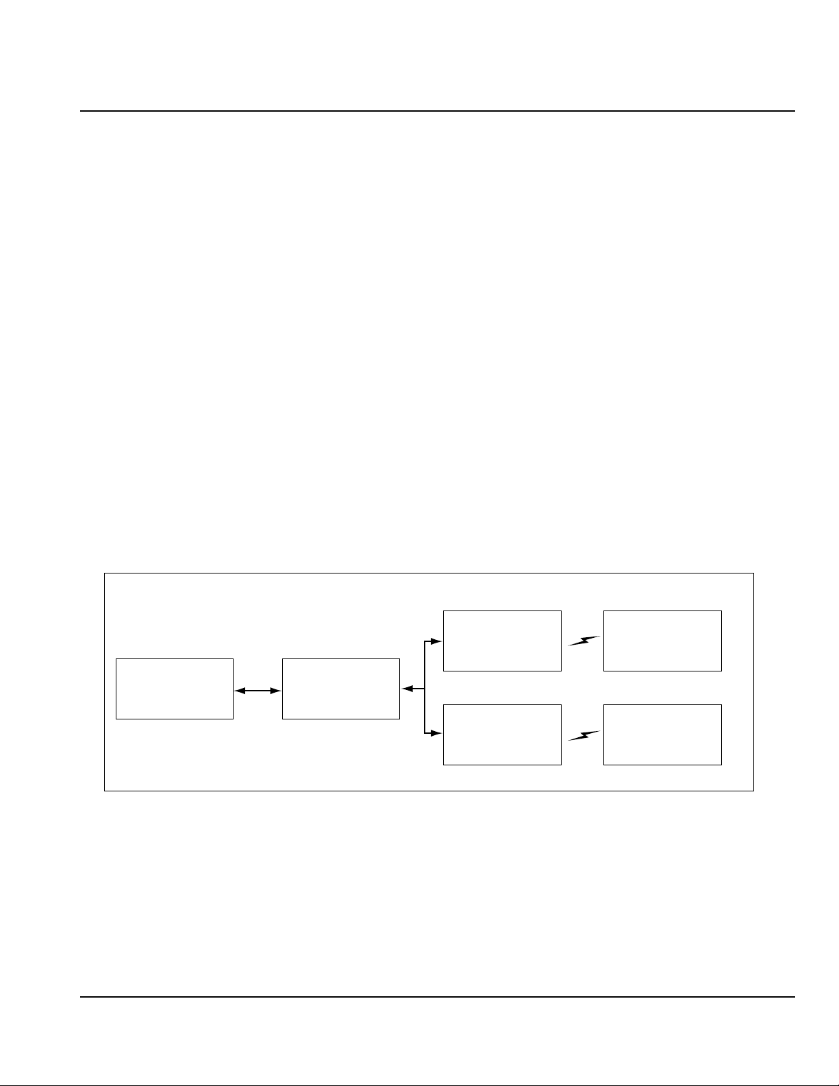
integrated into a product, is shown in
operation, contact your network operator (paging carrier).
Figure 2-7. For more details on network
-
Application
Host or Server
Network
Controller
Figure 2-7. Network Routing
Base Transmitter
or Base Receiver
Base Transmitter
or Base Receiver
(Specific Example)
Vending Machine
with Integrated
Data Transceiver
Host Product
with Integrated
Data Transceiver
(Generic Example)
807SRH-02
990007
July 23, 2002 2-16
Page 27

General CreataLink2 XT Hardware Integrator’s Guide
Air Interface
ReFLEX Network Operation
All two-way messaging networks that support two-way data communications with
CreataLink2 XT device use the ReFLEX protocol. The network can be viewed as
two separate one-way ne tworks. For messages dire cted to the data trans ceiver, the
network controller rout es the messages to one of many high po wer transmitter sites.
For messages from the data transceiver, a higher density of receiver sites are
provided to compensate for the lower transmit power of the data transceiver.
The Global Positioni ng System (GPS) synchroni zes the downlink and upl ink paths,
allowing downlink control of the uplink communications path. The network control
ler schedules all transmissions from the data transceiver for optimal utilization of
the uplink communications path.
Downlink messages are deli vered at a time when the data transceiver is guara nteed
to be listening, as de fined by the data transcei ver battery-save mode/colla pse value.
Each unit is assigned certain frames in which its messages can be received. The
personal address collapse and information services collapse values are used to
schedule those frames a uni t mus t deco de f or mess ag es. If y ou u se the se coll apse d
frames, you are trading battery life for the more frequent delivery of messages.
Therefore, collapse frame use provides a battery-save mode and defines the per
centage of the time the data transceiver is listening to the channel for messages.
The remainder of the time the data transceiver is in a low-power state, and is not
listening to the carrier channel for messages. It is important for the data transceiver
and network controller to remain synchronized in order for mes sages to be delivered
successfully.
-
-
The downlink is also referred to as the forward path. The uplink is also referred to
➧
as the reverse path.
2-17 July 23, 2002
Page 28

General CreataLink2 XT Hardware Integrator’s Guide
Product Functionality
Product Functionality
The data transceiver relies on system software for basic operational instructions,
and on configura tion parameter values to meet data transceiver and network
interface requirements.
Operating System
The data transcei ver operating system is based on the FLEX Kernel operating
system. It can be reloaded or upgraded by the service center. For third-party
software developers, tools are available to load in main operating code.
Power-up Operating Mode
The data transceive r operates in one of two power-up modes, depending on the
condition of the supply voltage. If the supply voltage is not present, the data
transceiver does not power up. Minimize cable length to limit the voltage drop across
the cable during RF transmissions.
Supply Voltage At or Below Minimum Voltage
If the supply voltage level is less than or equal to 4V, the condition is detected and
the data transceiver does not power up.
If the supply voltage is greater than 4V, but less than 5V, the data transceiver
powers up but the performance will not be optimal. In this state, the data trans
ceiver can still communicate with the resident host but:
• attempts to initiate messages are likely to fail.
• receive sensitivity is drast icall y affecte d.
• transmit power and the corresponding FCC spectral mask are degraded.
When the supply volt age rises above 5V, the data transcei ver turns on and the unit
sucessfully enters the message-search mode.
Adequate Supply Voltage
A normal power-up occurs when the supply volta ge is above 5V. The data transcei ver automatically enters the message-search mode.
Message-Search Operating Mode
The message-search mode is the data tr ansceiv er’s main operat ing mode . When it
powers up, the transceiver turns ON, and the unit begins to search for a valid
ReFLEX frame. When the unit detects what appears to be a valid ReFLEX frame,
it synchronizes with this channel and begins to decode the contents of the frame.
The unit then attempts to register with the network (if the auto-registration feature
is enabled). The default configuration is Regist ration Off (alway s considered reg is
tered). After successful registration, the un it begins normal message de coding and
searches for its assigned ReFLEX address(es).
If the data transceiver does not detect a valid ReFLEX frame wit hin approximately
1.5 minutes, the unit enters a low current cons umption mode. This mode conserves
power for a pre-programmed length of time. When the time has elapsed, the unit
attempts, once again, to acquire a valid ReFLEX frame. The unit alternates between
-
-
2-18 July 23, 2002
Page 29

General CreataLink2 XT Hardware Integrator’s Guide
Product Functionality
searching for a valid ReFLEX frame and low current mode until it detects a valid
ReFLEX frame.
If the data transceiver detects a valid ReFLEX frame and has become synchronized,
but does not detect its address, the unit stays on the channel. It continuously
decodes frame data and waits for its address(es).
Address Capability
The data transceiver can receive the following addresses:
• ReFLEX 25: 1 personal service address and 6 information service addresses
• ReFLEX 50: 2 personal service address and 1 information service address
Additionally, for the ReFLEX 50 network only, each information service address
can have up to 32 subaddresses.
Duplicate Message Detection
To ensure proper message delivery, the data transceiver detects and cancels
duplicate messages sent via the pagi ng system. If it finds a dupli cate message , the
data transceiver discards it in a manner transparent to the host application.
Message Deletion
Unit IDs
When all message slots are occupied, or unused message memory is insufficient,
the data transceiver deletes the oldest message to make room for a new message.
Read messages are deleted before unread messages.
The data transceiver contains the following user identification strings within the
codeplug:
• Serial number
• Electronic serial number (ESN)
The strings are unique to each data transceiver.
Serial Number
The serial number consists of ten bytes of data stored in the data transceiver
codeplug. It is factory-programmabl e only.
Electronic Serial Number (ESN)
The ESN consists of four bytes of data stored in the data transceiver codeplug. Each
data transceiver is equipped with a unique serial number which serves as the
reverse channel address of the data transceiver.
The serial number and ESN are data transceive r-specific. If the unit is changed for
service, these numbers als o change. Th e carrier must be notified to make the PIN
number point to the new serial number and ESN.
2-19 July 23, 2002
Page 30

General CreataLink2 XT Hardware Integrator’s Guide
Product Functionality
Message Storage and Lengths
Messages are s tored in approx imately 32 kbyte s of RAM. Messa ge downlink le ngth
is a maximum of 1 kbyte, and uplink length is a maximum of to 2 kbytes. Consult
your carrier to determine message lengths supported on the network (see " Handling
Large Messages", in Section 2 - Getting Started, in the Software Integrator’s Guide).
2-20 July 23, 2002
Page 31

General CreataLink2 XT Hardware Integrator’s Guide
Product Functionality
Acknowledgment of Received Messages
System Acknowledge
The data transceiver transmits an Acknowledge Transmission signal (ACK) to
acknowledge automatically the receipt of a message. The data transceiver also
transmits a Nega ti ve Ack nowl ed ge Tra nsmi ssi on si gnal ( NAK) whe n me ssage s are
not received correctly. If the data transceiver transmits a NAK, the system resends
the message.
Registration Request
Registration enables nat ionwide systems to t rack the data tran sceiver from region
to region. The sys tem then transmits messa ges only to that regi on. The Enable Auto
Registration codeplug option enables automatic registration. The default registra
tion is OFF, because it is considered always registered for fixed applications.
The data transceiver genera tes th e regi st rati on reques t mes sa ge an d the regist ra tion request ALOHA packet with the current zone on the following occasions:
• A valid zone change: The data transceiver monitors the Zone ID field in the
ReFLEX frame header. When it recognizes that the frame header has changed,
the unit automatically sends a registration message after a delay.
• Power-Up: The data transceiver automatically transmits a registration request
only if automatic registration is enabled. Automatic registration is only
required if the application is mobile. SmartSynch, Inc. does not recommend
automatic registration for fixed location installations.
• A change from out-of-range to in-range: When the data transceiver goes out of
forward-channel range, and then returns within forward-channel range, the
data transceiver automatically transmits a registration request after a delay.
-
Configuration Parameters
Data transceiver configuration data is categorized as follows:
• The service provider establishes the network-specific parameters for the data
transceiver configuration. Typically, parameters are constant for all like
devices on the network. The parameters include the default channel list, roam
ing parameters, and other service provider protocol-related parameters.
• Only the factory or authorized service depot sets fixed device-specific parameters. These parameters indicate the type of radio installed, the type of data
transceiver , and the hardware revision level. Significant configuration items in
this category include the ESN, device type, hardware revision level, protocol
type, and low voltag e thresholds.
PPS Utility
Product Family 91B Programming Software (PPS) is a configuration utility that
enables some codeplug options to be programmed into the data transceiver. This
application runs on a stand-alone PC with the Windows 95®, Windows 98®, or
Windows NT® operating environment. The PPS interacts with the data transceiver
via the serial port. Because the 22-pin connector that contains the serial I/O is not
standard, you must connect the DB9 connector on the interface kit or a custom cable
to the PC serial port. The Programming Software Guide-Integrators, listed in
"Related Publications", provides instructions for configuring data.
-
2-21 July 23, 2002
Page 32

General CreataLink2 XT Hardware Integrator’s Guide
Product Functionality
For user-configured items, see Programming Software Guide-Integrators, listed in
➧
"Related Publications."
End-User Application Software
To develop your own embedded application r efer to the Software I ntegrator’s Guide
listed in "Related Publications."
Serial Interface
External host devices communicate with the data transceiver across the serial
interface via the asynchronous Communication Linking Protocol (CLP
mands.
The data transceiver supports a default serial baud of 9600 bps, no parity, eight
data bits, one star t bit, and one stop bit. The host product must provide a full duplex
(both directions at the same time) pass-through link at this speed.
TM
) com-
Communication Linking Protocol (CLP)
The CLP application contains a set of commands that enable the host to send and
retrieve messages, retrieve and modify select configuration information, and re
trieve status info rmation from the data transc eiver. When longer transmissio ns are
required to transfer da ta, the XMODEM file-t ransfer protocol provides error check
ing during transmission across the serial link.
The CLP application provides general wireless messaging services that are independent of the underlying RF protocol.
For a detailed descri ptio n of se rvi ces prov id ed, s ee t he Communicati on Linking
Protocol R eference Man u al listed in "Related Publications.".
-
-
2-22 July 23, 2002
Page 33

INTEGRATION OVERVIEW
Page 34

Page 35

91B
CreataLink2 XT Hardware Integrator’s Guide Integration Overview
3Integration Overview
Contents
Contents
Integration Goal and Objectives . . . . . . . . . . . . . . . . . . . . . . . . . . . . . . . . . . . . . . . . . . . . . . . . . . . . . . . . . . . . . . . . . . . . . . 3-1
Usage Model . . . . . . . . . . . . . . . . . . . . . . . . . . . . . . . . . . . . . . . . . . . . . . . . . . . . . . . . . . . . . . . . . . . . . . . . . . . . . . . 3-1
Message Model . . . . . . . . . . . . . . . . . . . . . . . . . . . . . . . . . . . . . . . . . . . . . . . . . . . . . . . . . . . . . . . . . . . . . . . . . . . . . 3-1
Service Strategy . . . . . . . . . . . . . . . . . . . . . . . . . . . . . . . . . . . . . . . . . . . . . . . . . . . . . . . . . . . . . . . . . . . . . . . . . . . . 3-2
System Design of Integrated Product . . . . . . . . . . . . . . . . . . . . . . . . . . . . . . . . . . . . . . . . . . . . . . . . . . . . . . . . . . . 3-2
Hardware Design . . . . . . . . . . . . . . . . . . . . . . . . . . . . . . . . . . . . . . . . . . . . . . . . . . . . . . . . . . . . . . . . . . . . . . . . . . . 3-2
Power Supply . . . . . . . . . . . . . . . . . . . . . . . . . . . . . . . . . . . . . . . . . . . . . . . . . . . . . . . . . . . . . . . . . . . . . . . . . . . . . . 3-2
Antenna Configuration . . . . . . . . . . . . . . . . . . . . . . . . . . . . . . . . . . . . . . . . . . . . . . . . . . . . . . . . . . . . . . . . . . . . . . . 3-3
Software Applications Development . . . . . . . . . . . . . . . . . . . . . . . . . . . . . . . . . . . . . . . . . . . . . . . . . . . . . . . . . . . . 3-3
EMI and Desense Testing . . . . . . . . . . . . . . . . . . . . . . . . . . . . . . . . . . . . . . . . . . . . . . . . . . . . . . . . . . . . . . . . . . . . 3-3
Regulatory Approval . . . . . . . . . . . . . . . . . . . . . . . . . . . . . . . . . . . . . . . . . . . . . . . . . . . . . . . . . . . . . . . . . . . . . . . . . 3-3
Final Assembly Test . . . . . . . . . . . . . . . . . . . . . . . . . . . . . . . . . . . . . . . . . . . . . . . . . . . . . . . . . . . . . . . . . . . . . . . . . 3-3
Installation and Field Test . . . . . . . . . . . . . . . . . . . . . . . . . . . . . . . . . . . . . . . . . . . . . . . . . . . . . . . . . . . . . . . . . . . . 3-4
Customer Problem Isolation . . . . . . . . . . . . . . . . . . . . . . . . . . . . . . . . . . . . . . . . . . . . . . . . . . . . . . . . . . . . . . . . . . . . . . . . . 3-5
Wireline and Wireless Communications . . . . . . . . . . . . . . . . . . . . . . . . . . . . . . . . . . . . . . . . . . . . . . . . . . . . . . . . . . . . . . . 3-6
Power Conservation . . . . . . . . . . . . . . . . . . . . . . . . . . . . . . . . . . . . . . . . . . . . . . . . . . . . . . . . . . . . . . . . . . . . . . . . . 3-6
Network Communication . . . . . . . . . . . . . . . . . . . . . . . . . . . . . . . . . . . . . . . . . . . . . . . . . . . . . . . . . . . . . . . . . . . . . 3-6
Throughput . . . . . . . . . . . . . . . . . . . . . . . . . . . . . . . . . . . . . . . . . . . . . . . . . . . . . . . . . . . . . . . . . . . . . . . . . . . . . . . . 3-7
Design Tips for Serviceability . . . . . . . . . . . . . . . . . . . . . . . . . . . . . . . . . . . . . . . . . . . . . . . . . . . . . . . . . . . . . . . . . . . . . . . . 3-8
Data Transceiver Accessibility . . . . . . . . . . . . . . . . . . . . . . . . . . . . . . . . . . . . . . . . . . . . . . . . . . . . . . . . . . . . . . . . . 3-8
SmartSynch Software Utilities . . . . . . . . . . . . . . . . . . . . . . . . . . . . . . . . . . . . . . . . . . . . . . . . . . . . . . . . . . . . . . . . 3-8
Developing Diagnostic Software Utilities . . . . . . . . . . . . . . . . . . . . . . . . . . . . . . . . . . . . . . . . . . . . . . . . . . . . . . . . 3-8
Environmental Issues . . . . . . . . . . . . . . . . . . . . . . . . . . . . . . . . . . . . . . . . . . . . . . . . . . . . . . . . . . . . . . . . . . . . . . . . . . . . . . . 3-9
Coasting Performance . . . . . . . . . . . . . . . . . . . . . . . . . . . . . . . . . . . . . . . . . . . . . . . . . . . . . . . . . . . . . . . . . . . . . . . 3-9
General Precautions . . . . . . . . . . . . . . . . . . . . . . . . . . . . . . . . . . . . . . . . . . . . . . . . . . . . . . . . . . . . . . . . . . . . . . . . 3-10
ESD Precautions . . . . . . . . . . . . . . . . . . . . . . . . . . . . . . . . . . . . . . . . . . . . . . . . . . . . . . . . . . . . . . . . . . . . . . . . . . . 3-11
Regulatory Requirements . . . . . . . . . . . . . . . . . . . . . . . . . . . . . . . . . . . . . . . . . . . . . . . . . . . . . . . . . . . . . . . . . . . . . . . . . . 3-12
Overview . . . . . . . . . . . . . . . . . . . . . . . . . . . . . . . . . . . . . . . . . . . . . . . . . . . . . . . . . . . . . . . . . . . . . . . . . . . . . . . . . 3-12
Compliance . . . . . . . . . . . . . . . . . . . . . . . . . . . . . . . . . . . . . . . . . . . . . . . . . . . . . . . . . . . . . . . . . . . . . . . . . . . . . . . 3-12
June 18, 2002 3-i
Page 36

Integration Overview CreataLink2 XT Hardware Integrator’s Guide
Contents
3-ii June 18, 2002
Page 37

CreataLink2 XT Hardware Integrator’s Guide Integration Overview
3Integration Overview
Integration Goal and Objectives
Integration Goal and Objectives
SmartSynch, Inc. recommends that you consider the impact of each task on the
development plan and allow sufficient time for required activities. Try to identify
critical path activities early in product development. The following list summarizes
the development ta sks. These tasks are disc ussed in detail in the following chapters.
• Define a usage model.
• Define a message model that specifies how many messages will be sent/
received and how often.
• Define a service strategy.
• Define system design of integrated product
• Design the hardware.
• Consider power supply options.
• Identify the source antenna.
• Design, code, and t est an end-to-end application between the data transceiver
and host device.
• Obtain regulatory approval.
• Set up an assembly and final test environment.
• Perform a field installation functional verification procedure.
• Develop an in-the-field problem isolation test strategy and the necessary test
tools.
Usage Model
Message Model
As a developer, you must have, above all, a clear understanding of the end-use of
the product. End-use directs the devel opment process; all design considerations aim
to meet the needs of the final customer.
Design issues related to a mo bile device, such as altern ator noise and vibration and
handling of changing RF cond itions, are different from design issues required for a
fixed-point telemetry application powered by line power, battery, or solar panel.
End-user priorities should determine the critical engineering tradeoffs in the
product design.
You are responsible for defining the usage model. SmartSynch, Inc. is available to
provide assistance and answer questions but is not directly involved in this phase
of the project.
The message model is related to the usage model. Create the message model to
determine how much and how often d ata is sent in each of the up link and downlink
directions. Power supply requirements and network message routing selection
depend on this data determination. The amount of data sent and received is also
relevant in calculating the cost of airtime. Many engineeri ng decisions req uire the
message model as source data.
You are also responsible for defining the message model. A typical approach to
creating the message model is to define the peak and average throughput
requireme nts b ased on th e ty pe o f ap plic at ion. Take into acc oun t bo th no rmal and
unique conditions. Typical current consumption figures for each of the various
models of operation (transmit, receive, standby) are provided in this manual.
For ReFLEX networks, message latency is inherently longer than in circuitswitched connections. Use shorter messages to minimize latency and increase
reliability.
July 10, 2002 3-1
Page 38

Integration Overview CreataLink2 XT Hardware Integrator’s Guide
Integration Goal and Objectives
Service Strategy
The objective of the service strategy is to define processes by which to ident ify the
cause of a user’s problem and keep the customer operational during repair.
Diagnostics
It is best to test the data transceiver while it is integrated with the host at the user’s
site. To provide this function, the product must include a pass-through mode of
communications for the data transceiver. SmartSynch, Inc. recommends that you
incorporate a test mode that extracts details of the status of the data transceiver
in the host application.
Customer Support
For uninterrupted service, SmartSynch, Inc. recommends that you install a spare
unit and call the service provider to update its database with the spare unit
information. Return the defective unit to the SmartSynch, Inc. warranty repair
center for repair and return.
System Design of Integrated Product
Power source, RFI/EMI issues, and end-user environment are crucial
considerations that you must address while meeting CreataLink2 XT device
environmental and power supply requirements.
CreataLink2 XT device is a board-level product. It is your responsibility to protect
➧
the device from environmental hazards such as dust, rain, condensing humidity,
ESD, etc.
Hardware Design
To integrate a wireless data transceiver into a hardware design, you must consider
power supply, battery size (where applica ble), heat dissipation, isolation from EMI,
and physical mounting of the unit for proper groundi ng. SmartSynch, Inc. can
provide recommendations for hardware design, where applicable.
Power Supply
Power supply requirements vary according to the needs defined by the usage and
message models. Consider the following when you design a power su pply:
• Current drain of the data tra nsceiver in its various operating modes
• Ripple and noise on the power lines
• Supply instantaneous curren t (up to 1400 mA) to allow proper transmitter
operation (2.5 A supply if using the I/O)
These requirements define the type of power supply (linear or switched) to use with
the wireless d ata t rans cei ver. See Sec tion 2, Tabl e 2- 1 " Gene ral Spe cif icat ion s" for
power supply requirements.
3-2 July 10, 2002
Page 39

CreataLink2 XT Hardware Integrator’s Guide Integration Overview
Integration Goal and Objectives
Antenna Configuration
The data transceiver is available with an optional antenna from SmartSynch, Inc.
See Section 4, "Hardware Integration" for other antenna s uppliers.
Use the following guidelines when you mount the data transceiver:
• Mount the device away from any metallic or conductive enclosures.
• Mount the device away from items that produce RF noise, such as a poorlyshielded PC.
• Use an antenna with a gain of 0 dBi to +3 dBi to maximize the effective
radiated power (ERP) of the antenna.
• Mount the antenna according to the guidelines in Section 4.
• If you must mount the device in a metallic or conductive enclosure, mount the
antenna outside the enclosure and connect it to the data transceiver via the
female SMA connector with the coaxial cable (RG58).
Software Applications Development
In addition to the specific software application, SmartSynch, Inc. encourages you
to incorporate wireless-specific reporting and monitoring features into the
application, so as to make it more sensitive to the wireless environment
(registration states and messaging status information, for example). The data
transceiver uses a packetized serial interface (CLP) to enable the application to
monitor wireless link-related information and application-specific data
simultaneously. T he Communication Linking Pr otocol Reference Manual describes
this interface in more detail. If you use an on-board application configuration, the
required information is available via the API in the Software Integrator’s Guide.
EMI and Desense Testing
Data transceiver operation requires that there is minimum electromagnetic
interference radiating from the product platform. Exces s noise significantly reduces
the effectiveness of the wireless data transceiver, making it less likely to receive
network messages.
Regulatory Approval
Every commercial RF device must display an FCC regulatory label on the outside
host case. The FCC also requires the wireless data transceiver to transmit random
data patterns on specific freque ncies whi le incorpo r ated in the host platform. The
data transceiver incorporates special debug modes to help test for regulatory
compliance with this requirement. For most applications, no additional FCC
certification is required.
Final Assembly Test
To verify proper assembly of the final product (ant enna connection and opera tional
serial and/or parallel port) perform an end-to-end test. This test verifies that the
final product can receive and transmit at the required signal levels and has
operational I/O ports.
July 10, 2002 3-3
Page 40

Integration Overview CreataLink2 XT Hardware Integrator’s Guide
Integration Goal and Objectives
Installation and Field Test
A product shipped to a site might be mounted in a location that restricts RF
communications. To verify that the data transceiver is located in an area of good
coverage, and that an end-to-end loopback message is possible, the product needs
a software application to perform the test or a pass-through mode that enables a
message to be sent and received. Work with your carrier to determine exactly how
to do this on the network.
The most effective approach to field testing is to include an installation test
procedure as part of the standard host application software. SmartSynch, Inc. can
recommend the specific network information available from the data transceiver
and how to best implement an end-to-end loopback t est.
3-4 July 10, 2002
Page 41

CreataLink2 XT Hardware Integrator’s Guide Integration Overview
Customer Problem Isolation
Customer Problem Isolation
When a customer reports a pro blem from th e field, you must i solat e the so urce. To
isolate the prob lem, determine if it is the network , the wireless data transceive r, or
the host product that is causing the p roblem. Of ten, th e custo mer misunde rstands
the use of the product. Off-site troubleshooting reduces the number of returned
products and service costs, particularly if the host must be disassembled to remove
the data transceiver.
SmartSynch, Inc. recommends that the product application (both at the terminal
and host ends) incorporate diagnostic software that enables you to identify problems
from a remote site. One method is to incorporate progressively deeper loopback
tests. Use progressively longer message lengths to determine when the
communication link fails.
Make this diagnostic function part of the standard software load. SmartSynch, Inc.
can indicate the types of failure condition reporting mechanisms present in the data
transceiver and recommend implementations.
July 10, 2002 3-5
Page 42

Integration Overview CreataLink2 XT Hardware Integrator’s Guide
Wireline and Wireless Communications
Wireline and Wi reless Communications
Consider the similarities and differences between wireline and wireless
communications: Wireline data communications involve two data transceivers that
use a dial-up telephone link to send and rece ive da ta. This t ype of communi cati on
is known as "full duplex, circuit-switched communications." Full duplex indicates
both sides can send and receive simultaneously. Circuit-switched indicates the
sender and receiver have access to the entire communications line at all times
without sharing wit h ot her use r s. T he wirel ine me tho d o f co mmunicat ions wa stes
air time in a wireless setting because, typically, one side does mo st of the
transmitting while the other side is listening.
In wireless packet communications, the sender and receiver can share the
communication media with other users by sending packets, or bursts of data. This
method of communication enables other users to send their packets between the
gaps. To reduce data transmission cost, the communications are usually sent half
duplex; the sender does not listen while it transmits.
Some data communications protocols (XMODEM and YMODEM) are designed to
be used on a full dup lex, circuit-switched co nnection. The user p ays for the number
of minutes the circuit is open, regardless of the amount of data sent. Short timers,
numerous link level acknowledgments, and error correction help speed the data
transfer. With wireless packet data, the user is billed only for the data actually sent.
It makes more sense to consider communications in terms of datagrams ( similar to
what is used in IP). Much of the error correction and acknowledgment information
sent in wireline communications becomes an extra cost burden because the packet
data protocol already provides for forward error correction and link level
acknowledgments.
Determine which applications are best suited f or wireless and which applications
need to be modified before you use wireless. Message-based applications such as
database lookup, e-mail without attachments, and point-of-sale transactions are
suited to wireless communication, often without modification. Applications that
send handshaking messages or applications with timers that resend too quickly are
unsuitable for wireless communica tions because of the unnecessary overhead traffic
they generate.
Power Conservation
For installations that require power conservation (battery or solar cell powered),
consider data transceiver power consumption in the various operating states and
how data transceiver configuration affects power consumption. The data
transceiver uses the ReFLEX protocol battery-save cycle configuration, a customerordered option, for low po wer cons umption. To reduce ave rage power co nsumption
further, activate the data transceiver only when needed (see Table 2-3, "Power
Connection" section, and "Power Supply Circuit Details" section).
Network Communication
There are two ways to communicate with a network:
• Connection
• Connectionless
Most packet communication is connectionless and does not require call setup and
teardown for communications. For the most efficient airt ime solution, SmartSynch,
Inc. recommends a connectionless communications model.
3-6 July 10, 2002
Page 43

CreataLink2 XT Hardware Integrator’s Guide Integration Overview
Wireline and Wireless Communications
Throughput
The network throughput of the device de pends on several factors:
• Raw throughput of the radio channel
• Overhead involved in forward error correction
• Support for packet headers
• Number of active users on a shared RF channel
• Network configuration
July 10, 2002 3-7
Page 44

Integration Overview CreataLink2 XT Hardware Integrator’s Guide
Design Tips for Serviceability
Design Tips for Serviceability
Consider the concept of serviceability early in the design. Create a functional service
strategy that includes procedures fo r performing unit-level screening. The test must
determine whether a fault lies with the data transceiver or with the product into
which the data transcei ver is integrated. The test must also screen for network
problems and human error.
Data Transceiver Accessibility
Locate the data transceiver so that the serial I/O, parallel I/O, and antenna
connections are accessible. Quick access to the data transceiver enables easy
removal and installation, troubleshooting, and functional testing.
SmartSynch Software Utilities
SmartSynch, Inc. provides the programming software utility with which to
configure the data tran sceiver. The PPS operates with Windows 95, Windows 98 and
Windows NT and communicates via the RS-232 serial connection. For
microprocessor-based host pla tforms, provide a pass-through mode that enables the
programming software utility to run while the data transceiver is connected to the
end-user’s host design or system.
Developing Diagnostic Software Utilities
A thorough serviceability plan includes a needs assessment for developing software
utilities that help you to identify communication problems among the product, the
data transceiver, and the RF network. These utilities must send commands to the
data transceiver, evaluate responses, perform network connectivity testing, and
verify data communications with the network.
Develop these utilities via the CLP command set or the internal CLP API if you are
developing an on-board/embedde d application. The CLP API provides t he capability
to monitor and evaluate data transceiver operating conditions and all
communications to and from the wireless network host.
The CLP command set and CLP API supports reading of a diagnostic buffer that
provides the view of the network from the data transceiver. This utility is essential
for field service engineers and service center technicians attempting to diagnose
product problems, and trace such probl ems to failed assemblies or mismanaged
communications links. See the "Diagnostic Mode" subsection of the "Off-Board
Application Development" chapter in the Software Integrators Guide for details.
Pager to/from e-mail and pager-to-pager communication is supported in the
ReFLEX protocol, which SmartSynch, Inc. reco mmends for diagnostics. An example
of this feature is sending a message to a pager worn by the technician servicing the
equipment. This enables you to perform local troubleshooting.
3-8 July 10, 2002
Page 45

CreataLink2 XT Hardware Integrator’s Guide Integration Overview
Environmental Issues
Environmental Issues
The CreataLink2 XT device is designed as an OEM module. Any data transceiver
applications are house d i n a host p roduct . T he d ata trans cei ver ha s been t es ted t o
environmental specifications that meet the applications of most inte grators.
As an integrator, you must meet the following guidelines:
1. The data transceiver must be housed in an enclosure to protect the board
assembly from condensation and water/dust/salt fog intrusion. Any
condensation on board assembly will cause CreataLink2 XT device to be
non-functional.
2. Provide mechanical support of the PCB to withstand drops, transport stress,
and handling.
3. Power supply must be clean per Table 2-1.
4. Ambient air temperature around the CreataLink2 XT device must be
maintained between -40 degrees C and +85 degrees C.
Coasting Performance
Coasting is the process by which the data transceiver remains synchronized to the
ReFLEX network during periods when ReFLEX information (i.e. frames) is not
being received by the data transceiver. The absence of ReFLEX frames can be
caused by the data transcei ver being in an RF fade or by the network being
configured to intentionally st op transmi tting ReFL EX fra mes for a p eriod o f time .
Synchronization, in this case, has both timing and frequency elements.
Maintaining timing synchronization with the ReFLEX system is critical for both
network and data t ransceive r operation. When the da ta transcei ver has a me ssage
to transmit into the network, it first informs the network that it has data to send.
The network then schedules the data transceiver transmission and informs the data
transceiver of the specif ic time to tra nsmit its data. Failure on the part of the data
transceiver to remain very closely synchronized to the network will result in the
transmission occurring at an incorrect time and an in creased p robabilit y of a failed
message delivery.
Maintaining frequency synchronization is critical for both receive and transmit
operations on the data transceiver. Algorithms deployed in the data transceiver
firmware use received ReFLEX frames for frequency correction. Following the
absence of ReFLEX frames, should the tune d frequency of t he receive r drift too far
from the target, messages directed to the data transceiver will not be received.
Moreover, the network wi ll not receive messages transmitted by the data
transceiver if the frequency of the data transceiver transmitter has drifted out of
tolerance.
For a data transceiver in a constant ambie nt temperature environment, timing and
frequency errors are very small and can be largely ignored. However, in a dynamic
temperature environment, temperature variation of component tolerances can
cause synchronization to be lost. Algorithms in the data transceiver firmware have
been developed to track, predict, and correct both timing and frequency errors
within certain design limits.
A data transceiver in an open air environment (i.e. not in a housing) can maintain
timing and frequency synchronization with the network in the presence of a
temperature gradient not excee ding 1°C/minute. The addition of a housing a round
the data trans ceiver provides an insulating layer which re duces the grad ient of the
temperature change experien ced by t he co mponen ts on t he da ta tr anscei ve r PCB.
It is up to the integrator to select appropriate housing material and thickness, and/
July 10, 2002 3-9
Page 46

Integration Overview CreataLink2 XT Hardware Integrator’s Guide
Environmental Issues
or provide another mean s of insula ting the data transceive r sufficientl y to achieve
a temperature gradient at the board level not exceeding 1°C/minute.
General Precautions
Failure to provide adequate protection will void the device warranty.
G
Take the following general precautions to prevent damage to the data transceiver:
• Handle the data transceiver as little as possible.
• Wear a grounded antistatic wrist strap while you handle the data transceiver.
• Do not bend or stress the data transceiver.
• Insert connectors straight and evenly to avoid bending pins.
3-10 July 10, 2002
Page 47

CreataLink2 XT Hardware Integrator’s Guide Integration Overview
Environmental Issues
ESD Precautions
This data transceiver contains components that are sensitive to ESD. People
typically experience up to 35 kV ESD while walking on a carpet in low humidity
environments. Many electronic compone nts can b e damaged by few er than 10 00V
of ESD. Observe handling precautions when you service this equipment:
• Eliminate static generators (plastics, styrofoam, etc.) in the wo rk area.
• Remove nylon or double knit polyest er jackets , roll up long sl eeves , and remove
or tie back loose-hanging nec kties.
• Store and transport all static-sensitive components in ESD protective
containers.
• Disconnect all power from the unit before ESD sensitive components are
removed or inserted, unless otherwise noted.
• Use a static safeguarded workstation. Such safeguards includes a conductive
wrist strap, ground cords, and static control table mat.
When antistat ic facilities are not available, use the following techn ique to minimize
the chance of ESD damage to equipment:
• Place the static-sensitive components on a conductive surface when not in use.
• Make skin contact and maintain the contact with a conductive work surface
before you handle the static-sensitive component.
• Maintain relative humidity at 70%–75% in development labs and service
centers.
To eliminate electrostatic discharge to the 22-pin connector on Crea taLink2 XT
within the customer's product/application, it is recommended that the customer's
product does not place components within an extended keep out envelope of 15 mm
around the 22-pin connector.
July 10, 2002 3-11
Page 48

Integration Overview CreataLink2 XT Hardware Integrator’s Guide
Regulatory Requirements
Regulatory Requirements
This chapter provides guidance on how to obtain regulatory approval of products
that integrate the CreataLink2 XT data transceiver.
Overview
Worldwide, government regulatory agencies for communications have es tablished
standards and requirements for products that incorporate fixed, mobile, and
portable radio transmitters. To this end, SmartSynch, Inc. must certify the
CreataLink2 XT device in specific regional markets to levels of compliance
appropriate for an integrated device. Approvals are required for two in terrelated
reasons: to guard public safety and to ensure electrical noninterference.
The nonintegrated data transceiver meets the following FCC regulatory
requirements:
• FCC Part 90—Radio Performance
• FCC Part 15—Conducted and Emitted Radiation Class B
• FCC Part 24—NBPCS-Narrow Band PCS Transceivers
Compliance
SmartSynch, Inc. is responsible for testing and verifying that the CreataLink2 XT
device complies with all of the above FCC requirements. The process includes
extensive measurements such as conducted power-out, emission limits, spurious
emissions (conducted and radiated), RF hazard, and frequency stability over
temperature. The test data are compiled as a formal report and submitted to the
FCC for Type Acceptance certification. Once approved, all producti on CreataLink2
XT units are cleared for sale in the U.S., with the required product labeling.
The FCC requires the OEM host product to be labeled as follows:
At the time of this printing, this product contains a type-accepted
transmitter approved under FCC ID: E9698109. Contact SmartSynch at
www.smartsynch.com to get the latest FCC ID for current releases of
hardware.
Refer to FCC CFR 47, Part 2, Subpart J, for information on how to obtain an FCC
grantee code, FCC identifier requirements, label requirements, and other
equipment authorization procedures.
The FCC does not permit use of an FCC identifie r until a Grant of Equipment
Authorization is issued. If you display a device at a trade show before the FCC has
issued a grant, you must display the following statement prominently:
This device has not been approved by the Federal Communications
Commission. This device is not, and may not be, offered for sale or lease,
sold or leased until the approval of the FCC has been obtained.
Many countries in which th e final products are so ld require approval from the local
governmental regulatory bodies. In the U.S., the FCC requires that the following
two individual requirements are met before it certifies the final product:
• Test 1 is the familiar CFR 47, Part 15 qualification requiring proof that the
product electronics hardware does not yield local radiation that can affect
other equipment, such as TVs and computer monitors.
3-12 July 10, 2002
Page 49

CreataLink2 XT Hardware Integrator’s Guide Integration Overview
Regulatory Requirements
• Test 2 (CFR 47, Part 24 and 90) proves that the data transceiver remains in its
allocated channel spacing when it transmits, and does not produce spikes or
splatter in other frequencies. SmartSynch, Inc. undergoes FCC testing with
the data transceiver integrated into a dummy OEM host to ensure
conformance with these requirements.
According to the equipment authorization rules (CFR 47, Part 2), SmartSynch, Inc.
is allowed to authorize a second party to integrate the CreataLink2 XT into another
product, provided that the CreataLink2 XT device is unmodified and used as
intended. It is your responsibility to determine whether or not the integrator’s
electronics are subject to further FCC equipment authorization. Consult an
appropriate regulatory consultant or agency to determine your exact circumstances.
Once this determination is made, make the appropriate implementation:
• Integrator’s electronics ARE NOT subject to FCC equipment authorization:
Display the CreataLink2 XT device FCC ID, "FCC ID: E9698109", on the
common enclosure that houses the CreataLink2 XT devi ce and integrator’s
electronics. NOTE: Contact SmartSynch at www.smartsynch.com for the latest
FCC ID on current CreataLink2 XT hardware.
Or
• Integrator’s electronics ARE subject to FCC equipmen t authorization: Obtain
FCC approval for integrator’s electronics through all applicable FCC
requirements, in which case a unique FCC ID shall be assigned to the
electronics. Display the CreataLink2 XT device FCC ID, "FCC ID: E9698109"
and the integrator’s FCC ID on the common enclosure tha t houses the
CreataLink2 XT device and integrator’s electronics . NOTE: Contact
SmartSynch at www.smartsynch.com for the latest FCC ID on current
CreataLink2 XT hardware.
July 10, 2002 3-13
Page 50

Integration Overview CreataLink2 XT Hardware Integrator’s Guide
Regulatory Requirements
3-14 July 10, 2002
Page 51

HARDWARE INTEGRATION
Page 52

Page 53

91B
CreataLink2 XT Hardware Integrator’s Guide Hardware Integration
4Hardware Integration
Contents
Contents
Power Supply . . . . . . . . . . . . . . . . . . . . . . . . . . . . . . . . . . . . . . . . . . . . . . . . . . . . . . . . . . . . . . . . . . . . . . . . . . . . . . . . . . . . . 4-1
Line-Powered Implementation . . . . . . . . . . . . . . . . . . . . . . . . . . . . . . . . . . . . . . . . . . . . . . . . . . . . . . . . . . . . . . . . 4-1
Battery-Powered Implementation . . . . . . . . . . . . . . . . . . . . . . . . . . . . . . . . . . . . . . . . . . . . . . . . . . . . . . . . . . . . . . 4-2
Host Interface . . . . . . . . . . . . . . . . . . . . . . . . . . . . . . . . . . . . . . . . . . . . . . . . . . . . . . . . . . . . . . . . . . . . . . . . . . . . . . . . . . . . . 4-3
Power/Serial/Parallel I/O . . . . . . . . . . . . . . . . . . . . . . . . . . . . . . . . . . . . . . . . . . . . . . . . . . . . . . . . . . . . . . . . . . . . . 4-3
I/O Pin Interface . . . . . . . . . . . . . . . . . . . . . . . . . . . . . . . . . . . . . . . . . . . . . . . . . . . . . . . . . . . . . . . . . . . . . . . . . . . . 4-4
RX_Active and TX_Active Signal Behaviors . . . . . . . . . . . . . . . . . . . . . . . . . . . . . . . . . . . . . . . . . . . . . . . . . . . . . 4-11
Power Connection . . . . . . . . . . . . . . . . . . . . . . . . . . . . . . . . . . . . . . . . . . . . . . . . . . . . . . . . . . . . . . . . . . . . . . . . . . 4-16
Power Management . . . . . . . . . . . . . . . . . . . . . . . . . . . . . . . . . . . . . . . . . . . . . . . . . . . . . . . . . . . . . . . . . . . . . . . . . . . . . . . 4-17
States of Operation . . . . . . . . . . . . . . . . . . . . . . . . . . . . . . . . . . . . . . . . . . . . . . . . . . . . . . . . . . . . . . . . . . . . . . . . . 4-17
Power Profile . . . . . . . . . . . . . . . . . . . . . . . . . . . . . . . . . . . . . . . . . . . . . . . . . . . . . . . . . . . . . . . . . . . . . . . . . . . . . . 4-17
Backup Battery Power/Transmitter Power . . . . . . . . . . . . . . . . . . . . . . . . . . . . . . . . . . . . . . . . . . . . . . . . . . . . . 4-18
Power Supply Circuit Details . . . . . . . . . . . . . . . . . . . . . . . . . . . . . . . . . . . . . . . . . . . . . . . . . . . . . . . . . . . . . . . . 4-19
Shutdown Procedures . . . . . . . . . . . . . . . . . . . . . . . . . . . . . . . . . . . . . . . . . . . . . . . . . . . . . . . . . . . . . . . . . . . . . . . 4-19
Resetting the Data Transceiver . . . . . . . . . . . . . . . . . . . . . . . . . . . . . . . . . . . . . . . . . . . . . . . . . . . . . . . . . . . . . . . 4-20
Antenna Systems . . . . . . . . . . . . . . . . . . . . . . . . . . . . . . . . . . . . . . . . . . . . . . . . . . . . . . . . . . . . . . . . . . . . . . . . . . . . . . . . . 4-20
Antenna Safety . . . . . . . . . . . . . . . . . . . . . . . . . . . . . . . . . . . . . . . . . . . . . . . . . . . . . . . . . . . . . . . . . . . . . . . . . . . . 4-20
Antenna Selection Criteria . . . . . . . . . . . . . . . . . . . . . . . . . . . . . . . . . . . . . . . . . . . . . . . . . . . . . . . . . . . . . . . . . . 4-20
Antenna Mounting . . . . . . . . . . . . . . . . . . . . . . . . . . . . . . . . . . . . . . . . . . . . . . . . . . . . . . . . . . . . . . . . . . . . . . . . . 4-21
Antenna Location . . . . . . . . . . . . . . . . . . . . . . . . . . . . . . . . . . . . . . . . . . . . . . . . . . . . . . . . . . . . . . . . . . . . . . . . . . 4-21
Antenna Test Methods . . . . . . . . . . . . . . . . . . . . . . . . . . . . . . . . . . . . . . . . . . . . . . . . . . . . . . . . . . . . . . . . . . . . . . 4-21
Hardware Recommendations . . . . . . . . . . . . . . . . . . . . . . . . . . . . . . . . . . . . . . . . . . . . . . . . . . . . . . . . . . . . . . . . . . . . . . . 4-23
Antenna Connector . . . . . . . . . . . . . . . . . . . . . . . . . . . . . . . . . . . . . . . . . . . . . . . . . . . . . . . . . . . . . . . . . . . . . . . . . 4-23
Antenna Cable Assemblies . . . . . . . . . . . . . . . . . . . . . . . . . . . . . . . . . . . . . . . . . . . . . . . . . . . . . . . . . . . . . . . . . . 4-23
Antenna Assemblies . . . . . . . . . . . . . . . . . . . . . . . . . . . . . . . . . . . . . . . . . . . . . . . . . . . . . . . . . . . . . . . . . . . . . . . . 4-23
Antenna Dealers . . . . . . . . . . . . . . . . . . . . . . . . . . . . . . . . . . . . . . . . . . . . . . . . . . . . . . . . . . . . . . . . . . . . . . . . . . . 4-24
Battery Selection Criteria . . . . . . . . . . . . . . . . . . . . . . . . . . . . . . . . . . . . . . . . . . . . . . . . . . . . . . . . . . . . . . . . . . . . . . . . . . 4-25
Available Technologies . . . . . . . . . . . . . . . . . . . . . . . . . . . . . . . . . . . . . . . . . . . . . . . . . . . . . . . . . . . . . . . . . . . . . . 4-25
Applying Battery Technologies . . . . . . . . . . . . . . . . . . . . . . . . . . . . . . . . . . . . . . . . . . . . . . . . . . . . . . . . . . . . . . . 4-27
June 18, 2002 4-i
Page 54

Hardware Integration CreataLink2 XT Hardware Integrator’s Guide
Contents
4-ii June 18, 2002
Page 55

CreataLink2 XT Hardware Integrator’s Guide Hardware Integration
4Hardware Integration
Power Supply
Power Supply
SmartSynch, Inc. recommends a 2A power supply in the lab. This ensures sufficient
power to transmit. However, if the two driven output ports (pins 21 and 22 of the
22-pin connector) are utilized at their maximum rating of 350 mA sink/source
current and the six open collector I/Os are utilized at their maximum rating of 25
mA sink current, it will result in up to 850 mA of additional current consumed. A
power supply of 3A wo uld be required . A detailed overview of t he interface bo ard is
shown in
A rise time of 500 us is required on the 2A power supply when you power up the
➧
transmitter. The supply voltage can sag to 5V at this time, without impact to
transmitter operation.
Figure 4-1.
(Required for ICE Box
but not for JEENI Box)
3-Amp
Power Supply
Main
Power
ICE Box
Connect
Embedded
(This setup
enclosed in
the dotted box
is only used
for on-board
application
development)
Creatalink2 XT
SMA
JTAG
(Optional)
Serial
Protocol
Analyzer
22-pin Header
Ribbon Cable
JTAG Cable
PC or device
under test
DB-9
22-pin Header
Backup Batt. or
Transmit Supply
Backup
Power
Interface Board
JTAG Probe Blk Terminal Blk
Figure 4-1. Interface Board f or Off-Board Host Configuration or Software Development of Third Party
Embedded Application
Line-Powered Implementation
Line-powered configurations typically imply fixed-mount applications. A key design
consideration is the need to filter 60-Hz noise fr om the ac supply line, which ha s a
negative impact on data transceiver performance.
ICE or
JEENI
Box
990137-O
990006
The following design considerations are important when you install a fixed-mount
application:
• The dc power noise levels on the host interface to the 22-pin connector
July 23, 2002 4-1
Page 56

Hardware Integration CreataLink2 XT Hardware Integrator’s Guide
Power Supply
• Minimum operating voltage levels
• Shutdown procedures
• Device internal ambient temperature
• Antenna gain and proximity to user
• Repair and reprogramming facilities (pass-through mode of operation)
• Power outage and recovery issues, including the use of a backup batt ery
Battery-Powered Implementation
The CreataLink2 XT device can use battery power in three distinct ways.
Primary Power
Where there is no convenient access to ac l ine power, the data tra nsceiver must be
powered by a battery. In addition to the desi gn considerations noted previ ously, you
must also select an appropriate battery based on technology, capacity, and
operating limits.
The power supply voltage range is 5-12 Vdc for NUF3902 and 5-16 Vdc for
NUF8006. The power supply must be capable of supplying 1400 mA for
transmitter operation.
If no backup battery is connected or the backup battery lacks sufficient capacity,
AND the backup battery is used for transmitting, the following conditions
will result:
NUF8006: the unit will reset.
NUF3902: the unit will not transmit and will not reset.
RAM Backup Only
In this mode, a battery may be placed across pins 5 and 6 of the 22-pin connector.
When power on pins 1 and 2 fail, the CreataLink2 XT device automatically backs
up the contents of the RAM. This data will be available when primary power is
restored.
The battery voltage must be between 3 and 9 Vdc, and capable of supplying 1 mA.
RAM Backup and Transmitter/Receiver Supply
The NUF3902 CreataLink2 XT device can be configured via software to use the
main supply (pins 1 and 2 of the 22-p in co nnector ) or the batte ry/se condar y suppl y
(pins 5 and 6) for power. If the secondary supply is chosen, it will be used during
RF transmissions and while receiving. In addition, this voltage will be used to back
up the RAM contents in the event of a power failure.
The battery requirements in this case are the same as those listed in
Tables 2-1 and 2-3.
With this method of using the addi tional bat tery/alterna te power beside s the main
supply, the requirements of the pr imary supply change. The primary supply wou ld
be required to provide 65-90 mA for normal operation. I f required , I/O sou rcing an d
sinking currents would have to be added. As a result, this current could reach as
high as 1A.
The NUF8006 CreataLink2 XT is powered from the battery during RF
transmissions only when the Battery Transmit Option is used. With this
configuration, the main supply powers the CreataLink2 XT during Sleep and
Receive modes. The ba ttery requirements are the same as those li sted in
Tables 2-1 and 2-3.
4-2 July 23, 2002
Page 57

CreataLink2 XT Hardware Integrator’s Guide Hardware Integration
Host Interface
Host Interface
The CreataLink2 XT device has two connectors that interface with the host:
• Power/Serial/Parallel I/O
• I/O Pin Interface
Power/Serial/Parallel I/O
The 22-pin connector provides electrical power, serial communications, and I/O
capability to the data transceiver.
8- and 22-pin part numbers are listed in "Parts Information".
22-pin vertical head connector pin signals are shown in Table 4-1.
Table 4-1. 22-Pin Vertical Header Connector Pin Signals
Pin
Number
1
2
3
4
5
6
7
8
9
10
11
12
Signal Name Description
Supply
GND
TXDO
RS232_TXDO
BATT
BATT_GND
RXDI
RS232_RXDI
RESET_ENABLE
EXT_RESET
RX_ACTIVE
TX_ACTIVE
Power Supply Connection
Ground
3.3V TTL Serial Data from CreataLink2 XT
+/- 5V RS-232 Serial Data from CreataLink2 XT
Backup Battery / Alternate Transmit Power Supply
Ground
TTL Serial Data Received by CreataLink2 XT
RS-232 Serial Data Received by CreataLink2 XT
3.3V active-high input used to enable external
reset capability (no connect if no t used)
3.3V active-low input used to reset Crea taLink2 XT
(no connect if not used)
3.3V when CreataLink2 XT is receiving a page
3.3V when CreataLink2 XT is transmitting a page
13
14
15
16
17
18
A/D_EXT1
A/D_EXT2
HVIO_0
HVIO_1
HVIO_2
HVIO_3
July 23, 2002 4-3
Externally supplied analog input
Externally supplied analog input
Open collector output/High voltage input
Open collector output/High voltage input
Open collector output/High voltage input
Open collector output/High voltage input
NUF8006 only: Input Capture 2
Page 58

Hardware Integration CreataLink2 XT Hardware Integrator’s Guide
Host Interface
Table 4-1. 22-Pin Vertical Header Connector Pin Signals (Continued)
I/O Pin Interf ace
Pin
Number
19
20
21
22
Signal Name Description
HVIO_4
HVIO_5
HVIO_6
HVIO_7
Open collector output/High voltage input
Open collector output/High voltage input
Open collector output/High voltage input
NUF8006 only: Input Capture 1
Driven output/High volt a ge input
The CreataLink2 XT device pr ovide s many fe atures t hat yo u can confi gure to suit
the desired application. Such a configurable feature is the 8-bi t parallel I/O port.
Six of the eight bit s of this port are individually configurable as an open collecto r
output, or as an input. You can configure the remaining two bits as high current
driven outputs, or inputs. The desired configuration of this port is stored in
nonvolatile memory and is set upon power-up.
Maximum input voltage is specified as 12V for NUF3902 and 16V for NUF8006.
Maximum pull-up voltage is specified as 12V for NUF3902 and 16V for NUF8006.
The open collector outputs are capable of sinking 25 mA, and the driven outputs
are capable of sourcing/sinking up to 350 mA.
Table 4-1 shows a cross reference from signal name to corresponding pin number
on the 22-pin connector and each I/O pin’s potential functions.
High Voltage Input/Open Collector Output
Figure 4-2 is a view of the circuit and the relevant signals. The block on the right
reveals the necessary connections if the circuit is used as an open co llector output.
If used as an input, there are no external component requirements.
Pull-up Voltage
CreataLink2 XT
I/O Control
Switching
and
Low Voltage
Input/Output
Level
Shifting
Figure 4-2. High Voltage Input/Open Collector Output Circuit
Rpu
HVIO_0 -HVIO_5
LOAD
011210O
4-4 July 23, 2002
Page 59

CreataLink2 XT Hardware Integrator’s Guide Hardware Integration
Host Interface
High Voltage Input Circuit
There are no requireme nts fo r externa l comp onents, u nle ss the i nput vo lta ge i s to
be higher than 12V for NUF3902 and 16V for NUF8006. If this is the case, perform
external signal conditioning that will limit the voltage to a maximum of 12V for
NUF3902 and 16V for NUF8006. Logic ones on the input pin are read as logic ones
by the host processor, i.e. normal logic convention.
Over-voltage protection is not provided. ESD/transient protection is provided;
however, exceeding the specified maximum input voltages for long durations will
render the circuit nonfunctional.
The input voltage must be equal to or less than the supply voltage provided to
pin 1 of the 22-pin connector.
Open Collector Output Circuit
A pull-up resistor must be placed between the pull-up voltage and the connection t o
G
the CreataLink2 XT device. Otherwise, the circuit will fail.
To size the pullup r esistor, follow the steps detaile d in“Resistor Sizing Example” on
page 4-9. The maximum pull-up voltage for this circuit is specified as 12V for
NUF3902 and 16V for NUF8006.
Circuit Specifications/Limitations
The open collector circuit enables the CreataLink2 XT device to interface to systems
with higher voltages than it can support itself. This feature alone provides great
flexibility in interface circuit design. However, this circuit has some limitations that
you must recognize when you design. For example, the pull-up resistor must be
sized according to load size and desired output high voltage.
Current Sink Limitations
The CreataLink2 XT device has a maximum current sink capability of 25 mA when
the output is in the low state. To exceed this current co uld cause the circuit to break
down, thus causing a po tential failure. In a ddition, this co uld cause damage to th e
host processor, rendering the product non-functional. There is no sink current in
the high state.
To ensure that this maximum sink current is not exceeded, you must know the
circuit pull-up voltage, V
determines the lower-bound for the pull-up resistor, according to the following
relation:
R
Thus, for a system with V
ohms; for a system with V
ohms.
= (VPU)/(.025)
PUmin
, specification for the circuit. The pull-up voltage
PU
= 12V, the minimum value for R
PU
= 16V, the minimum value for R
PU
would be 480
Pumin
would be 640
Pumin
July 23, 2002 4-5
Page 60

Hardware Integration CreataLink2 XT Hardware Integrator’s Guide
Host Interface
Effect of Load Size on Pull-up Resistor
Figures 4-3 through 4-5 are plot s that show the effect of pul l-up and load resistances
on the output high voltage. The output low voltage is guaranteed to be less than
0.5V as long as no more than 25 mA is being sunk.
If a varying load is expected, select pull-up resistors to compensate for the range of
this variance. The figures depict simulation data that reflects how the output high
voltage is affected by a change in load resistance. Pull-up voltages for these plots are:
• 12V: Figures 4-3, 4-4, and 4-5 for NUF3902
• 16V: Figures 4-6, 4-7, and 4-8 for NUF8006
Output High Voltage with Load = 1K
Output High Voltage
Pull-Up Resistance (kohms)
990121
Figure 4-3. NUF3902: Output High Voltage versus Pull-up Resistance
4-6 July 23, 2002
Page 61

CreataLink2 XT Hardware Integrator’s Guide Hardware Integration
Host Interface
Output High Voltage with Pull-Up = 10k
Output High Voltage
Load Resistance (kohms)
990122
Figure 4-4. NUF3902: Output High Voltage versus Load Resistance
Output High Voltage with Pull=Up 1k
Load Resistance (kohms)
Figure 4-5. NUF3902: Output High Voltage versus Load Resistance
990123
July 23, 2002 4-7
Page 62

Hardware Integration CreataLink2 XT Hardware Integrator’s Guide
Pull-Up Resistance (kohms)
Host Interface
Output High Voltage with Load=1k
16.0
14.0
12.0
10.0
8.0
6.0
4.0
2.0
0.0
0.0 0.5 1.0 1.5 2.0 2.5 3.0 3.5 4.0 4.5 5.0 5.5 6.0 6.5 7.0 7.5 8.0 8.5 9.0 9.5 10.0
Figure 4-6. NUF8006: Output High Voltage versus Pull-up Resistance
Output High Voltage with Pull-Up = 10k
8
7
6
5
4
3
2
1
0
0.0 0.5 1.0 1.5 2.0 2.5 3.0 3.5 4.0 4.5 5.0 5.5 6.0 6.5 7.0 7.5 8.0 8.5 9.0 9.5 10.0
oad Resistance (kohms)
Figure 4-7. NUF8006: Output High Voltage versus Load Resistance
000166
000167
4-8 July 23, 2002
Page 63

CreataLink2 XT Hardware Integrator’s Guide Hardware Integration
Host Interface
Output High Voltage with Pull-Up = 1k
16
14
12
10
8
6
4
2
0
0.0 0.5 1.0 1.5 2.0 2.5 3.0 3.5 4.0 4.5 5.0 5.5 6.0 6.5 7.0 7.5 8.0 8.5 9.0 9.5 10.0
Load Resistance (kohms)
Figure 4-8. NUF8006: Output High Voltage versus Load Resistance
Resistor Sizing Example
In order to size the pull-up resistor properly, you must kno w the above parameters.
The following example demonstrates a suitable procedure for sizing the resistor.
System specifications:
VPU+ = 12V
V
RL = 10 kohms
+ VPU = pull-up voltage.
*V
First, you must determine the current required by the supply voltage in the high
state. The minimum load current in the high state, I
ILmin = VOHmin / RL = 1 mA
From this, determine the value of the pull-up resistor. Use the worst case
condition of 10V along with th e value of I
OHmin
OHmin
* = 10V
= Minimum voltage allowed on the output in the high state.
, is given by:
Lmin
determined above.
L
000168
RPU = (12V - 10V)/ ILmin = 2000 ohms
July 23, 2002 4-9
Page 64

Hardware Integration CreataLink2 XT Hardware Integrator’s Guide
Host Interface
This is well above the absolute min imum of 480 ohms determi ned above , thus you
will not encounter current sink problems. If better V
performance is desired,
Ohmin
this value can be lowered, with a lower bound given by the equation above.
This value for RPU can be cross checked to see if the system specifications can be
met. From the graph in
Figure 4-3, with a pull-up of 2000 ohms, the V
OHmin
will be
approximately 10V, thus the specification is met.
Now that you have determined the value of the pull-up resistor, you must determine
the required power rating of the pull-up resistor. This is governed by the pull-up
voltage and th e current passing th rough this r esistor w hen the ou tput is in the low
state.
P = (VPU) * (VPU / RPU) = 72 mW
From the above values, it would be recommended t o use a maximum value resi stor
of 2000 ohms with a 125 mW minimum power rating.
High Voltage Input/Driven Output Circuit
You can configure two of the programmable I/O lines, HVIO_6 and HVIO_7, as
high voltage inputs or high current source driven outputs.
Figure 4-9 diagrams the High Voltage Input/Driven Output circuit. All relevant
signals are depicted.
I/O Control
Low Voltage
Output
Low Voltage
Input
Figure 4-9. High Voltage Input/Driven Output Circuit
CreataLink2 XT Device
Switching
and
HVIO_6 -HVIO_7
LOAD
Level
Shifting
990125
Current Source Limitations
The driven output signals are capable of sourcing and sinking significant current
to their corresponding loads. Each of these two signals are capable of sourcing/
sinking up to 350 mA. Currents higher than this could cause permanent damage
to the circuit. The output high vo ltage provided by these two pins is approximately
equal to the voltage provided to pin 1 of the data transceiver’s 22-pin connector.
Thus, any unwanted noise on this line must be filtered before it is connected to the
CreataLink2 XT device, or on each individual output pin. When you design the
power supply for the CreataLink2 XT device, ta ke into account the se two I/O pi ns’
output current.
4-10 July 23, 2002
Page 65

CreataLink2 XT Hardware Integrator’s Guide Hardware Integration
Host Interface
Effect of I/O on Operating Current
The specification for the CreataLink2 XT device transmit current is 1400 mA.
However, if an application is to use the parallel I/O capabilities, this number could
nearly double. As a result, you should take into account the I/O when you design
the system power supply.
Open Collector I/O
As noted earlier, the open col lector lines are capable of sinking 25 mA each. This
current comes from the pull -up volt age, whi ch may o r may not b e the s ame supply
voltage as that applied to pin 1 of the 22-pin connector. If this is the same supply
voltage as the primary suppl y vol tage appli ed to t he Crea taL ink2 XT de vice, the n
you must account for this current.
Worst case occurs when all six open collector outputs are driven low and a re sinking
the maximum allowable current of 25 mA. This could result in as much as 150 mA
additional to the 1400 mA tra nsmit current.
Driven I/O
If the driven outputs are each sourcing their maximum current of 350 mA each,
then 700 mA must be added to the 1400 mA transmit current.
In the worst case, the CreataLink2 XT device is transmitting, while sinking the
maximum allowable for the open collector outputs, and sourcing the maximum
allowable with the driven output. This could bring the maximum peak current to
1400 + 6*25 + 2*350 = 2250 mA. SmartSynch, Inc. recommends at least a 2.5A
supply in this case.
The I/O current is a constant current and does not go down when the
CreataLink2
current would be 5 + 6*25 + 2*350 = 855 mA, with no valid RS-232 voltages present.
XT device is placed in the sleep mode. In this case, the worst case sleep
RX_Active and TX_Active Signal Behaviors
ReFLEX is a half-duplex, TDMA signalling protocol which means that the data
transceiver can either recei ve or transmit but not simultaneously. The TDMA
aspect means that the system uses time slots for synchronization in a manner
similar to a GSM system. In a ReFLEX system, the base timeslot is a 1.875 second
time slice, referred to as a frame. The data transceiver will wake up at the beginning
of a frame to listen to the channel and determine if there is a message in that frame
intended for that data transceiver.
In order to provide a lower average current, a method has been developed which
allows the receiver to be powered off for portions of time. A parameter named
Battery Save Cycle or Frame Collapse is provided which determines how often the
data transceiver has its receiver powered up. The data transceiver will power up
its receiver every (1. 875 * (2
3, then the data transceiver wil l power up its receiver ev ery 8 frames or 15 seconds
to look for a message. Each time the receiver is powered up, the RX_Active signal
is activated. When the rece iver is subsequently powered down, the RX_Act ive signal
is correspondingly deactivated.
Collapse
)) seconds. For example, if the collapse is set to
July 23, 2002 4-11
Page 66

Hardware Integration CreataLink2 XT Hardware Integrator’s Guide
Host Interface
There are two scena rios resulting from th e use of the battery save cycle. See Figure
4-10 illustrating the state of the RX_Active signal and receiver powerup state.
Scenario 1:
The data transceiver powers up its rece iver and there is no message being delivered.
In this case, the receiver will only be powered up for a small part of the entire frame.
Scenario 2:
The data transceiver powers up its receiver and a message is being delivered. In
this case, the receiver is left powered up long enough to receive the message.
RX_Active
Scenario 1-Wake up, Look for message, and go back to sleep
RX_Active
Scenario 2. Wake up, Receive message in Frame 1, and go back to
sleep
Fra me 1 Fra me 2 Fra me 3 F ra m e 4
Figure 4-10. Behavior of Receiver Active Line. Assumes collapse is 1 (Wake up every other frame)
A third, but unrelated, scenario which causes the receiver to be powered up is the
initiation of a transmission. The ReFLEX protocol requires that the data transceiver
be receiving at the start of the frame where a transmission will occur to ensure
synchronization to the system before it transmits. In this case, even if the data
transceiver is operat ing with a co llapse of 3 w here the da ta transce iver only wa kes
up every 8 frames, the receiver will be powered up before a transmission.
The behavior of the TX_ACTIVE line is similar. When the data transceiver is
actively transmitting a message, the TX_Active signal is activated. When the
transmission subsequently completes, the TX_Active signal is deactivated.
4-12 July 23, 2002
Page 67

CreataLink2 XT Hardware Integrator’s Guide Hardware Integration
Host Interface
Since the data transceiver must power up the receiver to synchronize before a
transmission, in all cases where a message is either received (and must be
acknowledged) or transmitted (and an acknowledgement will be received), there
will be a pairing of RX_Active and TX_Active signal activations. The amount of time
that the signals are active is dependent upon the amount of data transmitted. It is
possible for the data transceiver to both receive a message and transmit within the
same frame.
For most transmissions, the data transceiver must first transmit a system message
indicating a need to transmit to the system. The system will return a system
message to the data transceiver indicating in what frame and timing to begin its
transmission. Therefore, there will be a series of RX_Active and TX_Active
activations and deactivations when a message is being transmitted by the data
transceiver.
For messages transmitted using the TransmitShort CLP command or Transmit
Aloha Packet API call, the data transceiver is not required to obtain transmission
timing information from the system and can schedule its own transmission. In this
case, there will be a single RX_Active and TX_Active activation and deactivation.
July 23, 2002 4-13
Page 68

Hardware Integration CreataLink2 XT Hardware Integrator’s Guide
Host Interface
Some possible combination RX_Active/TX_Active scenarios are shown in Figure
4-11.
RX_Active
TX_Active
Scenario 1. Receiver wakes up and synchronizes to forward channel, and then
transmits in a frame where the receiver normally powers up
RX_Active
TX_Active
Scenario 2. Receiver wakes up and synchronizes to forward channel, and then
transmits in a frame where the receiver is normally powered down.
RX_Active
TX_Active
Scenario 3. Receiver wakes up and synchronizes to forward channel, receives a
message, and then transmits an acknoledgement in that frame.
Frame 1 Frame 2 Frame 3 Frame 4
Figure 4-11. Assumes collapse is 1 (Wake up every other frame)
4-14 July 23, 2002
Page 69

CreataLink2 XT Hardware Integrator’s Guide Hardware Integration
Host Interface
JTAG Communication Port
Table 4-2 shows a cross-reference b etween the signa l names and the cor responding
pin numbers on the data transceiver’s 8-pin JTAG connector.
Table 4-2. 8-Pin Vertical Header Connector Pin Signals
Pin
Number
1
2
3
4
5
6
7
8
Signal Name Description
B++
TMP1
ARM_TDI
ARM_TRST
ARM_TCK
GND3
ARM_TDO
ARM_TMS
ICE power source
Mode select
JTAG Data in
JTAG reset
JTAG clock
Ground
JTAG Data out
JTAG I/O
8- and 22-pin mating connector part numbers are listed in "Part Numbers".
July 23, 2002 4-15
Page 70

Hardware Integration CreataLink2 XT Hardware Integrator’s Guide
Host Interface
Power Connection
The host must provide power to the data transceiver as fol lows.
NUF3902: 5 Vdc to 12 Vdc
NUF8006: 5 Vdc to 16 Vdc. For NUF8006 current usage, see Table 2-3 and Figures
2-3 through 2-5.
All values in Tables 4-3 and 4-4 are approximate.
➧
T a ble 4-3. NUF3902 Current Usage
Current Transmit Receive Sleep
Typical 1150 mA 65 mA 3-4 mA
Maximum 1400 mA 90 mA 5 mA
a. CreataLink2 XT device operating currents only. I/O and
RS-232 currents must be added in to determine worst
case values.
Table 4-4. NUF3902 Transmit Output versus Supply Current
TX Power 0.5 W 0.75W 1.0W 1.5W 2.0W
Supply Current 0.61A 0.71A 0.81A 1.01A 1.17A
The numbers above reflect only the normal operating currents for the NUF3902
and NUF8006 CreataLink2 XT de vices. If the parallel I/ O port and RS-232 port are
to be used, the current draw due to these circuits must be included.
• The I/O port consists of six input/open collector outputs, and two input/driven
output lines. Worst case current occurs when the open collector lines are
configured as outputs and are driven low, while the driven outputs are driven
high. Each open collector output is capable of sinking 25 mA. Each driven out
put is capable of sourcing 350 mA. Assuming these worst case values, an additional (6 * 25) + (2 * 350) = 850 mA is possible.
• RS-232 communication requires 3-4 mA of supply current when valid RS-232
signal levels are present. There are two methods to eliminate this current.
1. Use TTL voltage l evels, and connect to pin 3 and pin 7 of t he 22-pin connect or.
a
-
2. Or, if RS-232 communication is a requirement, disable the host system’s
RS-232 transmitter when serial communication is inactive.
You must cons ider these specifications when you design the power sup ply. The
above scenario is a worst-case. Current usage varies based on operating modes and
I/O configuration.
You can adjust average current by selecting a custom battery save cycle option.
4-16 July 23, 2002
Page 71

CreataLink2 XT Hardware Integrator’s Guide Hardware Integration
Power Management
Power Management
Make power and ground electrical connections via the 2 2-pin conne ctor . Minimi ze
cable length to limit the voltage drop across the ca ble during RF transmissions.
The host must provide continuous dc power to the data transceiver. It resets if the
power source is interrupted. The data transceiver uses the built-in power-saving
capability of the ReFL EX protocol tha t enables it to spend the maj ority of the t ime
in the sleep mode.
States of Operation
The host power supply provi d es source current to the data transceiver. There are
four data transceiver power consumption states:
• Off—The data transceiver is off, or the host-supplied power has failed.
• Sleep—The processor is sleeping and wakes up to an interrupt, but the RF section is off.
• Receive— The processor is actively processing information. The RF sections
are on and de modulating data.
• Transmit—The processor is actively processing information. The RF sections
are on and transmitting data.
The data transceiver automatically powers up and enters the sleep or receive state
when supply voltage is applied.
Power Profile
Network Configuration System/Data Transceiver
Battery-Save Cycle
Both the network configuration and the data transceiver configuration affect the
percentage of time the Cre ataLink2 XT device spends in the slee p and receive states.
In a two-way paging network, the battery-save cycle is a configuration parameter
stored in the data trans ceiver and defined for the overall system.
Assume the system battery-save cycle parameter is ‘n’ and the data transceiver
battery-save cycle parameter is ‘m’. The data transceiver typically wakes up to
receive messages every 2
and the network schedules transmissions to the data transceiver at the times when
it is awake t o receive.
In situations where the outbound network loading is such that data transceivers
are required to be awake more often, the system can dynamically modify data
transceiver behavior. It can broadcast a system battery-save cycle that causes all
data transceivers to wake up for the lesser of every 2
For example, if the mode battery-save cycle parameter is 3 and the system batterysave cycle parameter is 7, then the data transceiver would wake up every 2
frames, and then revert to a sleep state. If the network determines that all data
transceivers on the network need to be awake more often, the network could
broadcast a system battery-save cycle parameter of 1. All pagers would respond by
waking up every 2
reduced, the network could broadcast a system battery-save cycle parameter of 7,
and the data transc eivers would rea ct by falling back to their own internal battery-
m
frames, where a frame takes place every 1.875 seconds,
n
frames or every 2m frames.
1
, or 2, frames to receive data. Once the system loading was
3
, or 8
July 23, 2002 4-17
Page 72

Hardware Integration CreataLink2 XT Hardware Integrator’s Guide
Power Management
save cycle parameter. Consult your network provider to de termine current network
parameters.
During frames when the CreataLink2 XT device is in receive mode, the receiver
only stays powered through part of the frame, unless the frame conta ins a message
for the CreataLink2 XT device.
Message Traffic Model
The message traffic model defines the number of messages transmitted and
received, and the average leng th of the messages sent and receiv ed in a given work
day. A dispatch application might have a message traffic model as follows:
• Messages transmitted in 8-hour day = 5
• Average length of transmission = 1 kbytes to 2 kbytes
• Messages received in 8-hour day = 10
• Average length of received message = 100 bytes to 200 bytes
This analysis of message traffi c provides the power consumption profile assessme nt
in terms of percentage of total time spent transmitting, receiving, and sleeping.
Use of Information Services
Some applications, such as a stock quotation broadcast service, require the use of
information services carried to t he data transceiver vi a additional addresses (IDs).
Each active service address, in a ddition to the data transceiver factory-loaded
personal address, increases the percentage of time the data t ransceiver stays in the
receive state, and increases the overall current consumption. However, this
addressing type provides a method by which to addre ss a group of Crea taLink2 XT
devices.
Backup Battery Power/Transmitter Power
The undervoltage reset circuit of CreataLink2 XT device senses a low voltage
condition almost instantaneously. In an undervoltage condition, the data
transceiver is reset, and all information in RAM is lost, including any unread
messages or pending message transmissions. A backup battery connected across
pins 5 and 6 of the 22-pin connector can prevent this loss. For RAM backup only,
this voltage is required to be at least 3 Vdc and a maximum of 9 Vdc.
In addition, you can connect pins 5 and 6 to a power source for use during RF
transmissions and whi le receiving. If these pins are to be used for this purpose, then
the requirements for the voltage on this pin change. For RF transmissions to occur
reliably, a voltage in the range of 5 Vdc minimum to 9 Vdc maximum must be
applied. This power source will be required to source as much as 1.4A during RF
transmissions.
4-18 July 23, 2002
Page 73

CreataLink2 XT Hardware Integrator’s Guide Hardware Integration
Power Management
Power Supply Circuit Details
You are responsible for supplying power to the data transceiver. Certain
specifications must be met to ensure proper operation.
The data transceiver accept s the f ol lowi ng range o f po wer su pply volt ag es ap plie d
to pin 1 (Supply) of the 22-pin connector:
NUF3902: 5 Vdc to 12 Vdc
NUF8006: 5 Vdc to 16 Vdc
The followin g additi onal spec ificati ons must also be met ( see Table 4-5 , Figure 4-1,
and Figure 4-2).
Table 4-5. Power Supply Specifications
Item NUF3902 NUF8006
Supply ripple–Vpp 100 mV peak-to-peak maximum up to 5 MHz
Open circuit voltage–Voc 12 Vdc maximum 16 Vdc maximum
➧
Shutdown Procedures
Rise time 500 µs or less (from 80 mA to 1400 mA)
Minimum voltage and current 5Vdc at 1.4A (without driven output current)
The voltage range describ ed in Table 4-5 is available in the integrator’s host system
in most applications. If the voltage is not available, use a regulator to ensure that
the supply voltage is 5 Vdc. Select the regulator based on the input volt age and
current-sourcing capabilities.
Switching regulators are efficient, but they introduce unwanted noise into the
system. If you use a switchi ng regulator, the filtered output should meet the suppl y
ripple specification.
Linear regulators supply a clean dc voltage but are inefficient. It is your choice
whether to use a linear or switching regulator.
A linear regulator is easier to integrate because of the quiet output.
If the host application turns the data transceiver off for any period of time,
SmartSynch, Inc. recommends that you send a reverse path message to the
application host or server indicating that the data transceiver is no longer available.
This prevents a failed message from being sent to a data t ransceiver that is powered
down. At power-up, send a message to the application server indicating that the
data transceiver is ready to receive messages.
July 23, 2002 4-19
Page 74

Hardware Integration CreataLink2 XT Hardware Integrator’s Guide
Antenna Systems
Resetting the Data Transceiver
There are three ways to reset the data transceiver:
• Remove and reapply power
• Issue the Set Power CLP command to the ON state. This results in a software-
generated reset (see Communication Linking Protocol Reference Manual)
or use the equivalent API call for on-board/embedded applications.
•Use the RESET_ENABLE and EXT_RESET pins on the 22-pin connector (first set
RESET_ENABLE/pin 9 high, th en set EXT_RESET/pi n10 lo w). After reset , set the
pins back to their original state, or the device will remain in reset.
Antenna Systems
This chapter describes how to select an antenna and incorporate it into a product
package. It is not within the scope of this document to include answers to questions
for every possible application. SmartSynch, Inc. recommends that you consult an
antenna design engineer to address individual application concerns.
Antenna Safety
When you design the antenna for a product that integrates the CreataLink2 XT
device, adhere to the following American National Standards Institute (ANSI)
safety criterion:
The design of the integrated product must be such that the location us ed
and other particulars of the antenna comply with the then current
American National Standards Institute (ANSI) Guidelines concerning
radio frequency energy exposure and with any other nationally
recognized radio frequency standards that may be applicable thereto.
Antenna Selection Criteria
Be aware of the fact that antenna selec tion, mounting, and location has a major
impact on communication performance. Bad antenna selection, mounting, or
location can result in very poor system communication performance.
The following are guidelines for good antenna selection:
Frequency range 896 MHz to 942 MHz band minimum
Polarization Vertical
Gain 0 dBi to +3 dBi
Normal Impedance 50 ohm
VSWR 1.75:1 maximum in the specified frequency range
It is recommended to use an antenna with a ground plane.
It is not recommended to use a high gain antenna for two reasons:
1. The Base Station transmitter and Base Station receiver are not collocated.
They may be in opposite directions.
2. By using a high gain antenna, you may be exceeding the FCC radiated
emissions limits.
4-20 July 23, 2002
Page 75

CreataLink2 XT Hardware Integrator’s Guide Hardware Integration
Antenna Systems
Antenna Mounting
1. It is not recommended to connect the antenna directly to the CreataLink2 XT.
2. Connect the antenna to the CreataLink2 XT using RG58/U coax cable (or
equivalent) of at least 3 feet in length.
3. Do not mount the antenna in close proximity to other antennas. Try to stay as
far away as practically possible. Separation of antennas must be at least three
feet. It is recommended to mount different antennas one a bove the other rather
than one besides the oth er. Coupling between ve rtically polariz ed antenna s is
minimal in the vertical direction.
4. For fixed wireless outdoor applications, mount the antenna as high as practically possible. Stay away from objects, especially metal objects.
5. For fixed wireless indoor applications, you must search for the best location.
As a general rule of thumb, mount the antenna four feet above the fl oor. Stay
away from wall s, and try to mount the ante nna in fro nt of an ex ternal w indow.
6. For vehicular applications, you must purchase an antenna that is designed to
be mounted in vehicles and meet the specific requirements listed in the
Antenna Selection Criteria. Follow the antenna manufacturer’s instructions
for antenna mounting.
Antenna Location
Antenna Test Methods
Finding the best location for the antenna is critical for overall system success. It is
especially critical in indoor application. You must search and find the best antenna
location that will result in successful communication.
The antenna performanc e must meet th e i mpedance a nd ma tc h the crit eria of the
data transceiver specification, and have the gain to meet the network ERP
requirements.
Perform the following two antenna tests to ensure the antenna meets requirements.
Integrate the antenna in its final form for both tests:
Impedance Match Test
Measure and verify that the nominal impedance and resulting VSWR, or return
loss, are within specifications (See Table 2-6).
Gain Test
Measure the gain with a test facility to ensure the ERP and pattern ripple are
acceptable. Pattern ripple is the gain deviation measured in a 360 degree polar plot.
A typical polar plot is shown (see
in one direction and zero gain in anot her. If the average gain is 1.5 dB, the ripple
is +/- 1.5 dB. Ripple is the measure of uniformity of gain. Most networks specify a
nominal gain and an allowable ripple.
Figure 4-12). The a ntenna could have 3 dB gain
July 23, 2002 4-21
Page 76

Hardware Integration CreataLink2 XT Hardware Integrator’s Guide
Antenna Systems
0
-1
-2
-3
-4
-5
-4
-3
-2
-1
0
Figure 4-12. Polar Plot Graphic
805SRH-24
805SRH-34
4-22 July 23, 2002
Page 77

CreataLink2 XT Hardware Integrator’s Guide Hardware Integration
Hardware Recommendations
Hardware Recommendations
An optional external antenna is avail able from SmartSyn ch, Inc. (see Table 6-1), or
the customer can supply the external antenna. The specifications for this
SmartSynch external antenna are listed in
Table 4-6. External Antenna Specifications
Property Description
Type Low profile with radome
Transmit frequ ency 896–902 MHz
Receive frequency 929–941 MHz
Impedance 50 ohms nominal
VSWR 1.5:1 maximum
Polarization Linear, vertical
Gain 0 dBi
Table 4-6.
Maximum power 5 watts continuous
Coaxial cable
Antenna Connector
The data transceiver connector is a standard female SMA connector. The mating
connector should be a standard male SMA connector.
Antenna Cable Assemblies
A variety of coaxial cable types can be used with standard male SMA connectors.
Use a double-shielded coaxial cable in noisy RF environments to provide the
necessary isolation from interference. In applications that require more than six
feet of coaxial cable, use a low loss coaxial cable.
Antenna Assemblies
The SmartSynch, Inc. external antenna assembly is a low-profile, omnidirectional
antenna that has six feet of double-shielded coaxial cable and a male SMA
connector. The antenna performs best with an additional ground plane
approximately eight inches in diameter, with the antenna centered.
6-foot long RG58/U, with SMA male
connector
July 23, 2002 4-23
Page 78

Hardware Integration CreataLink2 XT Hardware Integrator’s Guide
Hardware Recommendations
Antenna Dealers
Recommended antenna dealers are listed in Table 4-7.
Table 4-7. Antenna Dealers
Dealer Phone Number
Micro Pulse, Inc (805) 389-3446
Northpoint Communication Products, Inc. (919) 403-8598
Larsen Electronics, Inc. (800) 426-1656
Centurion International, Inc. (800) 228-4563
4-24 July 23, 2002
Page 79

CreataLink2 XT Hardware Integrator’s Guide Hardware Integration
Battery Selection Criteria
Battery Selection Criteria
This chapter provides an overview of the current state of available battery
technologies, and some considerations for applying battery technology to a packet
data product. Use batteries only if line power is unavailable.
Select a battery, based on the following factors:
•Cell size
• Internal impedance
• Charging requirements
• Susceptibility to common battery phenomena, such as memory effect or
overcharging
Available Technologies
The four prevailing battery technologies are:
• Nickel-Cadmium (NiCd)
• Nickel-Metal-Hydride (NiMH)
• Lithium Ion (Li-ion)
•Lead-Acid
Nickel-Cadmium
NiCd characteristics are as follows:
• Most mature technology
• Lower energy density (energy/volume) than NiMH or Li-ion
• Available in all cell sizes, including AA, 2/3A, 4/5A, A, 4/3A. This represents
the largest number of packaging opt io ns.
• Exhibits a memory effect when not discharged below the lower extent of its
operating voltage. The memory effect reduces the usable capacity of each
battery cell.
• Internal impedance of 25-30 mΩ for each 1.2V cell
• Cell voltages are 1.2V, with multiple cells used to obtain higher operating
voltages.
• Can withstand high current pulses that are characteristic of packet data
applications
• Typical charge method is -∆V (known as negative delta voltage). Negative delta
voltage mea ns charging the battery while waiting for the battery voltage to
peak and enter a slight overcharge condition, where the voltage actually begins
to decrease prior to terminating battery charging. NiCd is the most robust
battery technology available toda y for non-vehicular applications. NiCd
withstands overcharging, over-discharging, and harsh environments with
reasonable resilience.
• Raw battery cells or battery packs can be purchased from suppliers.
• Typical operating temperature range is –20° C to +50° C
Nickel-Metal-Hydride
NiMH characteristics are as follows:
• Reasonably mature technology with potential for improvements in battery
chemistry and energy density during the next five years
• Higher energy density than NiCd, but lower than Li-ion
• Available in standard sizes AA, 2/3A, 4/5A, A and 4/3A and some prismatic
(rectangular) configurations
July 23, 2002 4-25
Page 80

Hardware Integration CreataLink2 XT Hardware Integrator’s Guide
Battery Selection Criteria
• Exhibits the memory effect in a manner similar to NiCd technology, but at a
less pronounced level
• Internal impedance of 35–49 mΩ for each 1.2V cell
• Typical cell voltages are 1.2V, with multiple cells used to obtain higher
operating voltages.
• Earlier NiMH battery chemistry was damaged by high current discharge
pulses. This problem has been eliminated in recent battery chemistry. When
purchasing batteries of this type, determine if high current pulse discharging
is a concern.
• Typical charge method is dT/dt, where T is temperature. As the battery
reaches full charge, any further energy dissipates as heat. A temperature
threshold terminates the charge cycle in conjunction with voltage monitoring.
NiMH is more sensitive to overcharging that NiCD and exhibits decreased
capacity if repeatedly overcharged.
• Raw battery cells or battery packs can be purchased from suppliers.
• Typical operating temperature range is –10° C to +50° C.
Lithium-Ion
Li-ion characteristics are as follows:
• Less mature technology
• Higher energy density than either NiCd or NiMH
• Most suppliers do not sell cells, but force customers into particular solutions
through their battery pack designs. Due to cell lead times, purchasing cells to
design a battery pack could be a problem.
• Li-ion does not exhibit the memory effect and is not affected by partial discharging charging cycles.
• Internal impedance of 100–150 mΩ for each 3.6V cell. Li-ion batteries are susceptible to damage due to over-discharge and high current pulses.
Manufacturers recommend adding a protection circuit to battery pack des igns.
The resultant internal impedance of a battery pack with protection circuitry
can reach the 500 mΩ level.
• Typical cell voltages are 3.6V with multiple cells used to obtain higher
operating voltages.
• Li-ion ba tteries are very sensitive to over discharge and represent a hazard if
not properly designed with protection circuitry.
• Typical charge method is constant voltage, constant current.
• Typical operating temperature range is –10° C to +50° C
Lead-Acid
Lead-Acid characteristics are as follows:
• Very mature technology
• Low energy density
• Standard cells are available, but not in flashlight sizes
• No memory effect
• Internal impedance of 10-20 mΩ per 2V cell
• Typical cell voltages are 2.0 Vdc with multiple cells used to obta in higher
operating voltages.
• Typical charge method is to use a C/100 current source continuously on.
• Raw battery cells or packs are available.
• Typical operating temperature range is –30° C to +60° C.
4-26 July 23, 2002
Page 81

CreataLink2 XT Hardware Integrator’s Guide Hardware Integration
Battery Selection Criteria
Applying Battery Technologies
Review the following characteristics of packet data products when you consider
different battery technologies:
Inconsistent Current Drain
When battery manufactu rers specif y the ba ttery discharge profiles , they ass ume a
constant current drain model. In a packet data system, the constant current drain
model no longer applies. There are three levels of current drain states: sleep, receive,
and transmit. The data tr ansceiver cycles through these different states when
powered and in contact with the network.
To determine the realistic battery life or capacity for the pro duct, contact the battery
manufacturer or experiment by transmitting for different lengths of time.
Peak Currents During Transmissions
Because transmissions are short, view the resulting current drain during
transmissions as current pulses. Consider these pulses when you select the
appropriate battery technology.
Consider the internal impedance of the battery at the peak currents during
transmissions. This is when the largest voltage drop occurs across the battery
terminals. Design an adequate supply guard band to ensure that the data
transceiver and other circuitry in the final product are not reset during
transmissions.
Messaging Model
To determine the product batt ery capacity, define the messaging model for the
target market:
• Optimal number of hours by day, weeks, or months of use prior to recharge
• Number of messages transmitted per hour
• Number of messages received per hour
• Avera ge length of transmitted messages
Use the information and the current drains of the data transceiver and other
circuitry to define the requirements for battery supply voltage and capa city.
July 23, 2002 4-27
Page 82

Hardware Integration CreataLink2 XT Hardware Integrator’s Guide
Battery Selection Criteria
4-28 July 23, 2002
Page 83

TESTING
Page 84

Page 85

CreataLink2 XT Hardware Integrator’s Guide Testing
91B
5Testing
Contents
Contents
Hardware Integration . . . . . . . . . . . . . . . . . . . . . . . . . . . . . . . . . . . . . . . . . . . . . . . . . . . . . . . . . . . . . . . . . . . . . . . . . . . . . . . .5-1
Equipment . . . . . . . . . . . . . . . . . . . . . . . . . . . . . . . . . . . . . . . . . . . . . . . . . . . . . . . . . . . . . . . . . . . . . . . . . . . . . . . . .5-1
Enabler Functions . . . . . . . . . . . . . . . . . . . . . . . . . . . . . . . . . . . . . . . . . . . . . . . . . . . . . . . . . . . . . . . . . . . . . . . . . . .5-1
Specific Tests . . . . . . . . . . . . . . . . . . . . . . . . . . . . . . . . . . . . . . . . . . . . . . . . . . . . . . . . . . . . . . . . . . . . . . . . . . . . . . .5-1
Desense and EMI . . . . . . . . . . . . . . . . . . . . . . . . . . . . . . . . . . . . . . . . . . . . . . . . . . . . . . . . . . . . . . . . . . . . . . . . . . . .5-2
Application Software . . . . . . . . . . . . . . . . . . . . . . . . . . . . . . . . . . . . . . . . . . . . . . . . . . . . . . . . . . . . . . . . . . . . . . . . . . . . . . . .5-3
Software Driver Configuration . . . . . . . . . . . . . . . . . . . . . . . . . . . . . . . . . . . . . . . . . . . . . . . . . . . . . . . . . . . . . . . . .5-3
Network Configuration . . . . . . . . . . . . . . . . . . . . . . . . . . . . . . . . . . . . . . . . . . . . . . . . . . . . . . . . . . . . . . . . . . . . . . .5-3
Final Assembly . . . . . . . . . . . . . . . . . . . . . . . . . . . . . . . . . . . . . . . . . . . . . . . . . . . . . . . . . . . . . . . . . . . . . . . . . . . . . . . . . . . . .5-4
Installation . . . . . . . . . . . . . . . . . . . . . . . . . . . . . . . . . . . . . . . . . . . . . . . . . . . . . . . . . . . . . . . . . . . . . . . . . . . . . . . . . . . . . . . .5-5
Installation Overview . . . . . . . . . . . . . . . . . . . . . . . . . . . . . . . . . . . . . . . . . . . . . . . . . . . . . . . . . . . . . . . . . . . . . . . .5-5
Required Tools and Equipment . . . . . . . . . . . . . . . . . . . . . . . . . . . . . . . . . . . . . . . . . . . . . . . . . . . . . . . . . . . . . . . . .5-5
Installation Procedures . . . . . . . . . . . . . . . . . . . . . . . . . . . . . . . . . . . . . . . . . . . . . . . . . . . . . . . . . . . . . . . . . . . . . . .5-6
Troubleshooting . . . . . . . . . . . . . . . . . . . . . . . . . . . . . . . . . . . . . . . . . . . . . . . . . . . . . . . . . . . . . . . . . . . . . . . . . . . . . . . . . . . .5-9
End User Problem Resolution . . . . . . . . . . . . . . . . . . . . . . . . . . . . . . . . . . . . . . . . . . . . . . . . . . . . . . . . . . . . . . . . . . . . . . .5-10
Service Depot Repair . . . . . . . . . . . . . . . . . . . . . . . . . . . . . . . . . . . . . . . . . . . . . . . . . . . . . . . . . . . . . . . . . . . . . . . . . . . . . . .5-11
Screening . . . . . . . . . . . . . . . . . . . . . . . . . . . . . . . . . . . . . . . . . . . . . . . . . . . . . . . . . . . . . . . . . . . . . . . . . . . . . . . . .5-11
June 18, 2002 5-i
Page 86

Testing CreataLink2 XT Hardware Integrator’s Guide
Contents
5-ii June 18, 2002
Page 87

CreataLink2 XT Hardware Integrator’s Guide Testing
5Testing
Hardware Integration
Hardware Integration
Follow relevant engineering standards, requirements, and specifications to ensure
a proper integration effort. Functional tests performed during development validate
that the integrated product performs as designed.
Equipment
Table 5-1 shows the equipment needed to test the data transceiver.
Table 5-1. Recommended Test Equipment
Item Part Number/Description Source
Enabler Functions
Communication
analyzer
Spectrum analyzer 2.9 GHz capability Commercial Item
Protocol analyzer HP 4959 or equivalent Commercial Item
PC
Power supply HP E3610A Commercial Item
Oscilloscope 500 MHz, digital storage Commercial Item
Digital multimeter Standard range Commercial Item
To test the in teraction betwee n the data transc eiver and host, i nclude the follo wing
features:
• The capability to turn on and off the various host hardware components. This
capability helps to isolate possible desense and other emissions problems.
• The capability to pass information through the host between the data
transceiver and the test platform. This enables external programming and
configuration software to communicate wit h the data transceiver while
integrated with the host. For microprocessor-based products, accomplish
pass-through mode via software emulation that involves the host processor,
and passes full-duplex serial port information to and from the integrated data
transceiver.
HP 8920A or HP 8921A with option 01
(high stability time-base oscillator) for
taking test measureme nts
486DX66 or equivalent with 9-pin serial
port
Commercial Item
Commercial Item
Specific Tests
In addition to various tests that exercise your own circuitry (such as power-on
self-test), you must design tests that ensure proper interaction between the data
transceiver and the host. The following require evaluation:
• RF immunity—Ensure the RF transmissions of the data transceiver do not
interfere with operation of the host.
• Electrical signaling—Ensure the power sources and interface are functionally
compatible between the host and the data transceiver.
• Physical parameters—Ensure the physical configuration of the data
transceiver provides adequate ventilation, mounting, shielding, and grounding.
July 23, 2002 5-1
Page 88

Testing CreataLink2 XT Hardware Integrator’s Guide
Hardware Integration
• Antenna performance—Ensure the integrated antenna system meets the
required ERP specifications, VSWR specifications, and antenna propagation
patterns.
• ESD requirements—Ensure the host design protects the data transceiver from
electrostatic discharge.
• RF Re-radiation—Ensure the host does not allow spurious emissions in excess
of 60 dBc, caused by carrier re-radiation.
Desense and EMI
Any device with which the data transceiver i ntegrates can generate enough EMI to
reduce the ability of the data transceiver to receive at certain frequencies.
The ability to turn on and turn off various circuits in the data receiving device
provides identification and analysis of the components that cause desense. This
approach to desense troubleshooting can shorten the integration effort. It is critical
that you consider the data transceiver shielding early in the design phase.
5-2 July 23, 2002
Page 89

CreataLink2 XT Hardware Integrator’s Guide Testing
Application Software
Application Software
The data transceive r resides b etween t he appli cati on and the ne twork . Tests nee d
to verify the communications links between an external host and the data
transceiver and between the data transceiver and the network.
Software Driver Configuration
This test verifies that the driver software and configuration are such that the
external host and data transceiver serial port can communicate with each other.
Network Configuration
Determine if the application can use the data transceiver to communicate with a
two-way paging network. This test uses existing network software to communicate
with a specific network.
To ensure that the final application is able to respond correctly under all adverse
network conditions, the application software needs systemat ic testing against all
possible failure and exception conditions. Low battery, out of range, host down,
unexpected data, maximum message size, and maximum peak/sustained
throughput must not cause the host application to fail. Each condition must have
a specific remedial action.
July 23, 2002 5-3
Page 90

Testing CreataLink2 XT Hardware Integrator’s Guide
Final Assembly
Final Assembly
Before any product is shippe d, a final a ssembly test s hould be pe rformed to ensure
that all components are working properly and have been checked for loose
connections and proper software load. In this test, the data transceiver sends and
receives messages to it self or another data transcei ver or two-way p ager of the size
used in the application. Successful return of the message demonstrates that the
product is able to transmit and receive correctly.
5-4 July 23, 2002
Page 91

CreataLink2 XT Hardware Integrator’s Guide Testing
Installation
Installation
This chapter describes how to install the CreataLink2 XT device. Procedures are
for basic external antenna installation.
Installation Overview
The data tra nsceiver is a small, easy-to-operate pro duct that requires c omparatively
Table 5-2). A
G
little space. Installation requires common tools and equipment (see
dimensional drawing is provided (see Figure 5-1).
Follow the installation procedure and guidelines as specified. Failure to follow directions could
cause the unit to function improperly and/or cause the unit to become non-compliant with
FCC regulations.
• Mount the unit in an area that is as free of EMI as possible; away from noisy
digital supplies and control lers . Do not mount the u nit near me tallic object s , or
where it would be subjected to constant vibration.
• Ensure that the voltage supply i s well- regulate d; free from exces sive ripple and
voltage spikes. The ripple specification is 100 mV peak-to-peak up to 5 MHz.
The voltage supply should not drop below 5V for transmit/receive capability.
• Mount the external antenna in such a way as to prevent people coming within
twelve inches of it, per FCC RF hazard regulations.
Required Tools and Equipment
The tools and equipment req uired for installation are listed in Table 5-2.
Table 5-2. Tools and Equipment List
Item Type Purpose/Use
Drill with .138-inch (#28)
Drill and Bit
Mounting
Standoffs
Wrench 3/4-inch open-end
Template Provided
drill bit
1/2-inch drill bit To drill holes for external antenna (PTAF1001A).
4 Richco Standoffs p/n
SCBSM-3-01 and nuts p/n
HN6-32-01 (or some other
standoff to mount in
0.128- inch PCB holes).
To drill holes in mounting surface for data transceiver.
To connect data transceiver to mounting surface.
End-user can design a different mounting scheme for
integrating PCB assembly into the end product.
To tighten optional external antenna mounting nut to
antenna.
To mark mounting surface for data transceiver locating
holes (see
Figure 5-1).
July 23, 2002 5-5
Page 92

Testing CreataLink2 XT Hardware Integrator’s Guide
Installation
Installation Procedures
Ensure that there is no do or opening and closin g interference before yo u mount the
CreataLink2 XT device, if applicable.
Mounting
Mount the data transceiver to a rigid, flat surface using 4 standoffs or customerdeveloped enclosure appr opriate for environment (i.e. maintaining temperature
around the board assembly to -40 deg. C to +85 deg. C and ensuring that
condensation, and water/dust/salt fog intrusion does not occur).
External Antenna Assembly
1. Select a mounting surface that is as high as possible, flat, clean, and at least
eight inches in diameter. For optimal antenna performance, the mounting
surface should be metal.
2. Drill a 1/2-inch hole in the center of the mounting surface.
Drill the mounting surface hole close enough to the data transceiver location so that
➧
the cable can reach it.
G
Do not cut coaxial cable. Changing the length could degrade antenna performance.
Insert coaxial cable through the mounting s urface hole un til the external antenna
lies flush on the mounting surface.
3. Install the lockwasher and mounting nut. Tight en to a snug fit with a 3/4-inch
wrench. Do not overtighten.
CreataLink2 XT Data Transceiver Installation
Mount the CreataLink2 XT device using the following steps or develop your own
enclosure appropriate for the end-use environment.
1. Use the dimensions gi ven in Figure 5-1 (1.457 inches and 3.464 inches) to mark
the mounting location. All the dimensions in Figure 5-1 are in inches.
2. Drill four 0.138-inch (#28 drill bit) mounting holes.
3. Position the Cre ataLink2 XT data tr ansceiver and install the Richco Standoffs
(or other equivalent standoffs to be inserted into the 0.128-inch PCB holes). Do
not overtighten the hex nuts.
5-6 July 23, 2002
Page 93

CreataLink2 XT Hardware Integrator’s Guide Testing
Installation
1.748
1.457
0.128
0.724
0.023
0.145
0.302
0.066
Pin 2
Pin 1
0.049
G
1.277
3.464
3.740
0.382
0.386
0.138
0.252
000162-O
Figure 5-1. Dimensional Drawing
Seat the SMA mating connector properly. Overtightening the connector could cause permanent
damage to the data transceiver.
4. Connect the coaxial antenna cable to the data transceiver SMA connector.
Tighten the cable connector at 4-8 in-lbs. of torque (i.e. fi nger-tight only)
(see Figure 2-6).
Power, and Serial Cable Connection
5. Connect the cables and the power supply to the CreataLink2 XT board
assembly for end-use (see Top of Figure 2-6).
July 23, 2002 5-7
Page 94

Testing CreataLink2 XT Hardware Integrator’s Guide
Installation
Use a common ground between the CreataLink2 XT data transceiver power ground
➧
and the host machine.
Verifying the In stallation
To verify that the data transceiver can rece ive and initiate mess ages, use the hos t
system built -in test mode if availab le. If a bu ilt- in test m ode is not a vaila ble, use a
palmtop or laptop comput er wi th a tes t applica tion to prompt the data tran sceiver
to initiate and read messages. Use the following protocols:
• The host system initiates a message directed to another two-way
communicator to verify network operation.
• The data transceiver initiates multiple messages to itself to verify the
capability to send and receive messages.
• Initiate messages from the internet, e-mail, or another two-way communicator
to the data transceiver .
5-8 July 23, 2002
Page 95

CreataLink2 XT Hardware Integrator’s Guide Testing
Troubleshooting
Troubleshooting
Before you perform detailed troubleshooting, check for faults in the external power
source, including fuses, circuit breakers, and interlocking safety switches
(see Table 5-3).
Problem Fault Isolation
1. Check all interface cables for secure connections. Repair or replace as required.
No power up
2.
1. Check continuity of 22-pin connector at data transceiver connection.
Check 22-pin connector pin 1 for Supply voltage (NUF3902: 5-12 Vdc and
NUF8006: 5-16 Vdc).
Table 5-3. Troubleshooting
Verify that the proper pins are being used for communication (pins 3 and 7 for TTL
and 4 and 8 for RS232)
Check to see that a null modem type connection is being used for Rx/Tx serial
communication
Check connection at antenna and connection at the CreataLink2 XT data transceiver
SMA connector.
No serial I/O
No transceiver over
the air (OTA)
communications
2.
3.
1. Check registration status using proper CLP protocol command.a
2. If not registered, check out-of-range status using proper CLP protocol command.
3.
4. Make sure LED is blinking, indicating power
5. Check backup battery voltage/alternate power if used as transmit supply
6. Verify that your TX_SUPPLY in the codeplug is configured as desired
a. Refer to the Communication Linking Protocol Reference Manual listed in "Related Publications"
a
July 23, 2002 5-9
Page 96

Testing CreataLink2 XT Hardware Integrator’s Guide
End User Problem Resolution
End User Problem Resolution
It is time-consuming and expensive to have a unit returned to the service depot
when a temporary network or host outage may have caused the problem. Is the
problem caused by the host application, data transceive r, ne two r k, configuration,
or user error? Design the application to identify the source of end-user problems.
This functio n can be designed wi th the guidance o f SmartSynch, Inc. or the network
operator.
Tests need to provide a systematic, positive acknowledgment from each of the
network components:
• Data transceiver must be able to communicate wit h the external application
device. If so, it will respond to a properly formatted Get Configuration CLP
command.
• Data transceiver must be able to detect the network.
Issue a Get Status CLP command. If the status information indicates the unit is in
range, the data transceiver is detecting the system. For on-board applications, a
method of extracting service information must be pr ovided.
At initial start-up, the data transceiver assumes that it is within range. It takes
➧
approximately four minutes to determine that it is not within range.
• Data transceiver must be registered and allowed to operate on the network.
Auto-Registration is disabled (default). Transmit a short message to another pager.
Issue a Get Status CLP command and track the me ssage progress unt il the message
is delivered or fails to be delivered.
Auto-Registration is enabled. Issue a Get Status CLP command. If the status
information indicates unit registration, the data transceiver can operate on the
network.
• The host application must be up and running.
Identify the cause of the problem in the field. This avoids having to send the device
to the service depot when the problem was not caused by the devi ce. Design the
application so that the end user can identify the most likely cause of the problem,
and refer to a help desk for a quick solution.
5-10 July 23, 2002
Page 97

CreataLink2 XT Hardware Integrator’s Guide Testing
Service Depot Repair
Service Depot Repair
This chapter describes tests that you can perform on a unit that is sent to you for
service. These te st s we re de si gned to hel p yo u deter mi ne the spe cif ic p rob le m an d
decide whether to send them to SmartSynch , Inc. for repair. An end-to- end or loopback test involves all elements of the network and the data transceiver.
Screening
Screening requires the following operational items:
• RS-232 cable/power supply
• PC or other device that supports the CLP
• A protocol analyzer t o view communicati ons be tween th e data trans ceive r and
the external device
The objective is to test the suspect unit in a known, stable environment in which
all other components are known to be operational:
1. Connect the data transceiver to a PC or other device that supports the CLP,
and apply power.
2. Determine if there is a serial problem with the data transceiver:
• Issue the CLP Get Configuration command (see Communication
Linking Protocol Reference Manual for more information).
• The data transceiver responds to the command by sending a block of
configuration information.
• If the data transceiver does not respond, check cable connections, baud
(configurable), and word format (must be 8- bit, no parity).
• If not successful, the unit has a problem with the serial port.
3. Determine if the data transceiver detects the network:
• Wai t appro xi mat el y six mi nutes t o al low t he dev ic e ti me t o ac kn owl edg e
the system and th en iss ue th e Ge t St atu s com m an d (se e
Communication Linking Protocol Reference Manual for more
information).
• The data transceiver responds with a block of status information. The
fourth byte of the stat us in format io n is th e out -of -ra nge in dica to r. If this
location contains an ASCII 1, the unit is not detecting the system and is
out of range. This implies a problem with the receiver.
4. If the data transceiver detects the network, determine if the network detects
the data transceiver:
• The 17th byte of the status information is the registration information.
If this byte contains an ASCII 0, the unit is not registered. This indicates
a problem with th e address programmed in the unit, the transmitter, or
the configuration of the unit information in the network database.
5. If the data transceiver and the network ac knowledge each other it should be
possible to tran smit and receive messages:
• Issue the Transmit Me ssage CLP command, (see Communication
Linking Protocol Reference Manual
addressing information configured to send the message to the
CreataLink2 XT data transceiver initiating the message.
• Repeatedly issue the Get Status command, (see Communication
for more information), with the
Linking Protocol Reference Manual for more information), until byte
2 of the status information returned by the data transceiver indicates
success (bit3-bit1 = 100), or failure (bit3-bit1 = 010).
July 23, 2002 5-11
Page 98

Testing CreataLink2 XT Hardware Integrator’s Guide
Service Depot Repair
• If the message was successfully sent, the data transceiver should receive
the message. Bytes 13 and 14 of the status information returned by the
data transceiver is the number of non-downloaded messages. This
number increments as messages are received by the u ni t.
• Repeat this test several times to ensure messages are being s ent and
received correctly. If the unit is successfully sending the messages, but
the messages are not received until the unit transmits another message
or resets, then there is a battery-save configuration problem.
• To retrieve the messages, issue the Download Delete CLP command (see
Communication Linking Protocol Reference Manual for more
information).
5-12 July 23, 2002
Page 99

PARTS INFORMATION
Page 100

 Loading...