

isvi IC-M29 User Manual
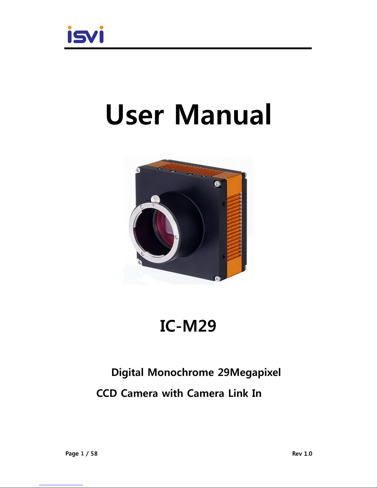
IC-M29
Page 1 / 58
Rev 1.0
User Manual
IC-M29
Digital Monochrome 29Megapixel
CCD Camera with Camera Link Interface
IC-M29
Page 2 / 58
Rev 1.0
Revision History
Revision Descriptions
0.1 Draft
0.2 Added Serial Communication specification
0.3
Added Camera control tool(GUI)
Fixed Minor errors
0.4 Fixed Minor errors
0.5 Fixed Minor errors
0.6
Updated function information
Updated Serial Communication Command
Updated Camera Control Tool(GUI)
Added Grabber(Matrox DCF File) Setting
Added Firmware Writing
Fixed Minor errors
0.7 Updated Camera Control Tool(GUI)
0.8 Fixed Minor errors
0.9
Updated Camera Control Tool(GUI) Rev 1.1D
Added M72 Mount Camera
1.0 Fixed Minor errors
IC-M29
Page 3 / 58
Rev 1.0
- Table of Contents -
1. Precautions
.................................................................................................................................................. 6
1.1 General
........................................................................................................................................................ 6
1.2 Precautions in Use
................................................................................................................................ 6
1.3 Maintenance
............................................................................................................................................ 6
2. Overview
......................................................................................................................................................... 7
3. Specification
............................................................................................................................................... 7
3.1 Electrical specification
........................................................................................................................ 7
3.2 Electrical shutter specification
....................................................................................................... 8
3.3 Mechanical spec
..................................................................................................................................... 8
3.4 Input signal specification
................................................................................................................. 8
3.5 Operating ambient conditions
...................................................................................................... 9
3.6 Various safety standards
.................................................................................................................. 9
3.7 Sensor Spectral Response(Quantum Efficiency) Information
................................... 10
3.7.1 Spectral response Mono
................................................................................................... 10
4. Camera Interface
................................................................................................................................ 10
4.1 General Description
.......................................................................................................................... 10
4.2 CameraLink Connector
.................................................................................................................... 12
4.3 Camera Link Interface
..................................................................................................................... 13
4.4 Power Input Connector
.................................................................................................................. 13
4.5 Control Connector
............................................................................................................................. 13
4.6 Trigger Input Circuit
........................................................................................................................... 14
4.7 Strobe Output Circuit
...................................................................................................................... 15
5. Functions and Operations
.......................................................................................................... 15
5.1 Basic Functions
.................................................................................................................................... 15
5.2 Trigger operation
................................................................................................................................. 15
5.2.1 free Run Mode
....................................................................................................................... 15
5.2.2 Trigger Mode/Master/Slave
.............................................................................................. 16
5.2.3 Overlap Mode
........................................................................................................................... 17
5.3 Gamma Correction(LUT)
................................................................................................................... 18
5.4 Defective Pixel Correction
............................................................................................................... 18
IC-M29
Page 4 / 58
Rev 1.0
5.5 Flat Field Correction
........................................................................................................................... 18
5.6 Test Pattern Image
.............................................................................................................................. 19
5.7 Region of interest(ROI)
..................................................................................................................... 19
5.8 Binning
....................................................................................................................................................... 20
6. External Appearance and Dimensions
.............................................................................. 21
7. Communication specification
.................................................................................................... 22
7.1 Communication Setting
.................................................................................................................... 22
7.2 Command Format
................................................................................................................................. 22
7.3 Command List
........................................................................................................................................ 22
7.3.1 Readout Mode
....................................................................................................................... 22
7.3.2 ROI Horizontal Area
........................................................................................................... 23
7.3.3 ROI Vertical Area
.................................................................................................................. 23
7.3.4 Binning Mode
......................................................................................................................... 23
7.3.5 Data Bits
.................................................................................................................................... 23
7.3.6 Test Pattern Enable
............................................................................................................. 23
7.3.7 LUT Mode
................................................................................................................................. 24
7.3.8 Reset
............................................................................................................................................ 24
7.3.9 Defective Pixel Correction
............................................................................................... 24
7.3.10 Flat Field Correction
......................................................................................................... 24
7.3.11 Flat Field Offset
.................................................................................................................. 24
7.3.12 Generate Flat Field Data
................................................................................................ 24
7.3.13 Save Flat Field Data
......................................................................................................... 25
7.3.14 Trigger Mode
....................................................................................................................... 25
7.3.15 Overlap Mode
...................................................................................................................... 25
7.3.16 Trigger Source
..................................................................................................................... 25
7.3.17 Trigger Polarity
................................................................................................................... 25
7.3.18 Exposure Time
..................................................................................................................... 26
7.3.19 Strobe Out Offset
.............................................................................................................. 26
7.3.20 Strobe Out Polarity
.......................................................................................................... 26
7.3.21 VGA Gain
................................................................................................................................ 26
7.3.22 VGA Gain Offset
................................................................................................................. 26
7.3.23 Optical Black Clamp Level
............................................................................................ 27
7.3.24 Optical Black Clamp Level Offset
............................................................................. 27
7.3.25 Config Initialization
.......................................................................................................... 27
7.3.26 Load & Save Config
......................................................................................................... 27
IC-M29
Page 5 / 58
Rev 1.0
7.3.27 Current Temperature
....................................................................................................... 27
7.3.28 MCU Version
........................................................................................................................ 28
7.3.29 Model Number
................................................................................................................... 28
7.3.30 FPGA Version
....................................................................................................................... 28
7.4 Storage Area
........................................................................................................................................... 29
7.5 Sensor Area Define
............................................................................................................................. 29
8. Camera Control Tool(GUI)
............................................................................................................ 30
8.1 Camera Connect
.................................................................................................................................... 30
8.2 User work space
.................................................................................................................................... 31
8.3 Main Tab
................................................................................................................................................... 32
8.4 Trigger Tab
.............................................................................................................................................. 36
8.5 Gain Tab
..................................................................................................................................................... 37
8.6 Gamma Tab
............................................................................................................................................. 39
8.7 FFC/DPC Tab
........................................................................................................................................... 40
8.8 Temperature Monitor
........................................................................................................................ 41
9. Grabber(Matrox DCF File) Setting
........................................................................................ 42
9.1 Overview Tab
.......................................................................................................................................... 42
9.2 Camera Tab
.............................................................................................................................................. 43
9.3 Video Signal Tab
................................................................................................................................... 46
9.4 Video Timing Tab
................................................................................................................................. 47
9.5 Pixel Clock Tab
....................................................................................................................................... 48
10. Firmware Writing
............................................................................................................................... 49
10.1 For Firmware write requirements
............................................................................................. 49
10.1.1 Hardware
................................................................................................................................... 49
10.1.2 Software
..................................................................................................................................... 50
10.2 Firmware writing
................................................................................................................................ 54
10.2.1 Cable Connection & writing
........................................................................................... 54
IC-M29
Page 6 / 58
Rev 1.0
1. Precautions
1-1. General
■ Do not drop or damage the device
■ Do not disassemble, repair or alter the device
■ Keep the machine not to be stained with the alien substances
■ Contact your nearest distributor in case of trouble or problem.
1-2. Precautions in Use
■ Do not expose the camera’s image-pickup-plane to sunlight or other intense
light directly. Its inner CCD sensor might be damaged.
■ In clearing, do not splash water on the device but wipe it out with smooth
cloth or towel.
■ Do not place magnets near the product.
■ Be careful not to let liquid like water, drinks or chemicals leak inside
the device.
■ Clean the device often to remove dust on it.
■ If the camera is not in use, attach the lens cap to the camera to protect the
Image Pickup surface
.
1-3. Maintenance
Turn off power to the equipment and wipe it with a dry cloth.
If it becomes severely contaminated, gently wipe the affected areas with a soft
Cloth dampened with diluted neutral detergent. Never use alcohol, benzene,
thinner, or other chemicals because such chemicals may damage or discolor the
paint and indications. If the image pickup surface becomes dusty, contaminated,
or scratched, consult your sales representative.
IC-M29
Page 7 / 58
Rev 1.0
2. Overview
IC-M29 is a mono area scan CCD camera.
IC-M29 has 29 million pixels resolution.
These Cameras are suitable for a wide range of application within factory
Automation, an also for application outside the factory floor, such as
AOI(Automatic Optical Inspection), High-end surveillance and medical.
Main Function
1) ROI(Region of interest)
2) DPC(Defective Pixel Correction)
3) FFC(Flat Field Correction )
4) Binning
5) VGA(Variable gain amplifier) Gain Control
6) Black Clamp Level Control
7) Gamma Control
8) Mode : Trigger Master Mode / Trigger Slave Mode / Free Run Mode
9) Image Data Output & Speed Selectable
10) Exposure Time Control
11) Test Pattern
12) External Trigger Support / External Strobe Output Support
13) Temperature Monitoring
3. Specification
3.1 Electrical specification
■ Image Sensor : Truesense KAI-29050 29M CCD image Sensor(Global Shutter)
■ Number of active pixels : 6576(H) x 4384(V)
■ full resolution in continuous operation : 5 frames/second [2Tap Base]
■ Pixel size : 5.5μm (H) × 5.5μm (V)
■ Optical size : 35mm Optical Format
■ Active Sensor Size : 36.17mm(H) x 24.11mm(V)
■ Number of Output : Quad
■ Sensitivity : 34uV / e-
■ ADC resolution : 8bit / 10bit / 12bit Raw Bayer Pattern Output
■ S/N Ratio : 55dB Over
IC-M29
Page 8 / 58
Rev 1.0
■ Dynamic Range : 64dB
■ Full Well Capacity : 20000 e-
■ Operating Temp : 0℃ ~ +40℃(Performance assurance)
■ Humidity : 20% ~ 90% RH(Non Condensing)
■ Camera Link Configuration : 2Tap Camera Link Base Mode
■ Built in LUT (Look Up Table)
■ Defective Correction Circuit built in
■ Pre-select and pulse width trigger modes
■ Power supply voltage : DC12 V ± 10%(ripple 50 mV or less) / MAX 15W
■ LVAL-synchronous / A-synchronous operation (auto-detect)
■ Setup by Windows XP / VISTA / WIN7 serial communication
3.2 Electrical shutter specification
■ Shutter Speed :
-. Exposure Time is 100μsec to 7000msec
-. Factory default : 10ms
■ Random Trigger Shutter (Factory default : Fixed Mode)
-. Fixed mode : The exposure time depends on the shutter speed setting
-. Pulse width mode : The exposure time depends on the pulse width.
-. Minimum pulse width : 100μsec(Minimum exposure time: 100μsec)
3.3 Mechanical spec
■ Lens mount : F Mount / M72 Mount
■ Dimensions : F Mount 97mm(L) * 97mm(W) * 86mm(H)
M72 Mount 97mm(L) * 97mm(W) * 77mm(H)
■ Weight : Approx 1.0kg
■ Camera body grounding : Conductive between circuit GND and camera body
3.4 Input signal specification
■ TRIG : Camera Link I/F(CC1) and External Control connector input
-. Signal level : TTL level
-. Polarity : High/Low switching (Factory default: Active-High)
-. Pulse width : 100μsec or more
IC-M29
Page 9 / 58
Rev 1.0
3.5 Operating ambient conditions
■ Performance assurance
-. Temperature : 0℃ to +40℃
-. Humidity : 20% ~ 90% RH(Non Condensing)
■ Operation Temperature(Image & Life cycle cannot guarantee)
-. Temperature :0℃ to +70℃
-. Humidity :10% to 90%(No dew formation)
■ Storage Temperature
-.Temperature : -20℃ to +70℃
-. Humidity : 90% or less (No dew formation)
3.6 Various safety standards
■ Performance assurance
-.CE(AoC)
Test Standard(2004/108/EC) : EN55022:2006 +A1:2007 [Class A Equipment]
EN 55024 : 1998 +A1:2001, +A2:2003
-.FCC(Verification)
Test Standard : Section 15.107, Section 15.109 (Class A Equipment)
NOTE : This equipment has been tested and found to comply with the limits for
a Class A digital device, pursuant to part 15 of the FCC Rules. These limits are
designed to provide reasonable protection against harmful interference when
the equipment is operated in a commercial environment. This equipment
generates, uses, and can radiate radio frequency energy and, if not installed
and used in accordance with the instruction manual, may cause harmful
interference to radio communications. Operation of this
equipment in a residential area is likely to cause harmful interference in which
case the user will be required to correct the interference at his own expense.

IC-M29
Page 10 / 58
Rev 1.0
3.7 Sensor Spectral Response(Quantum Efficiency) Information
3.7.1 Spectral response Mono
Fig 3.1 Spectral response
4. Camera Interface
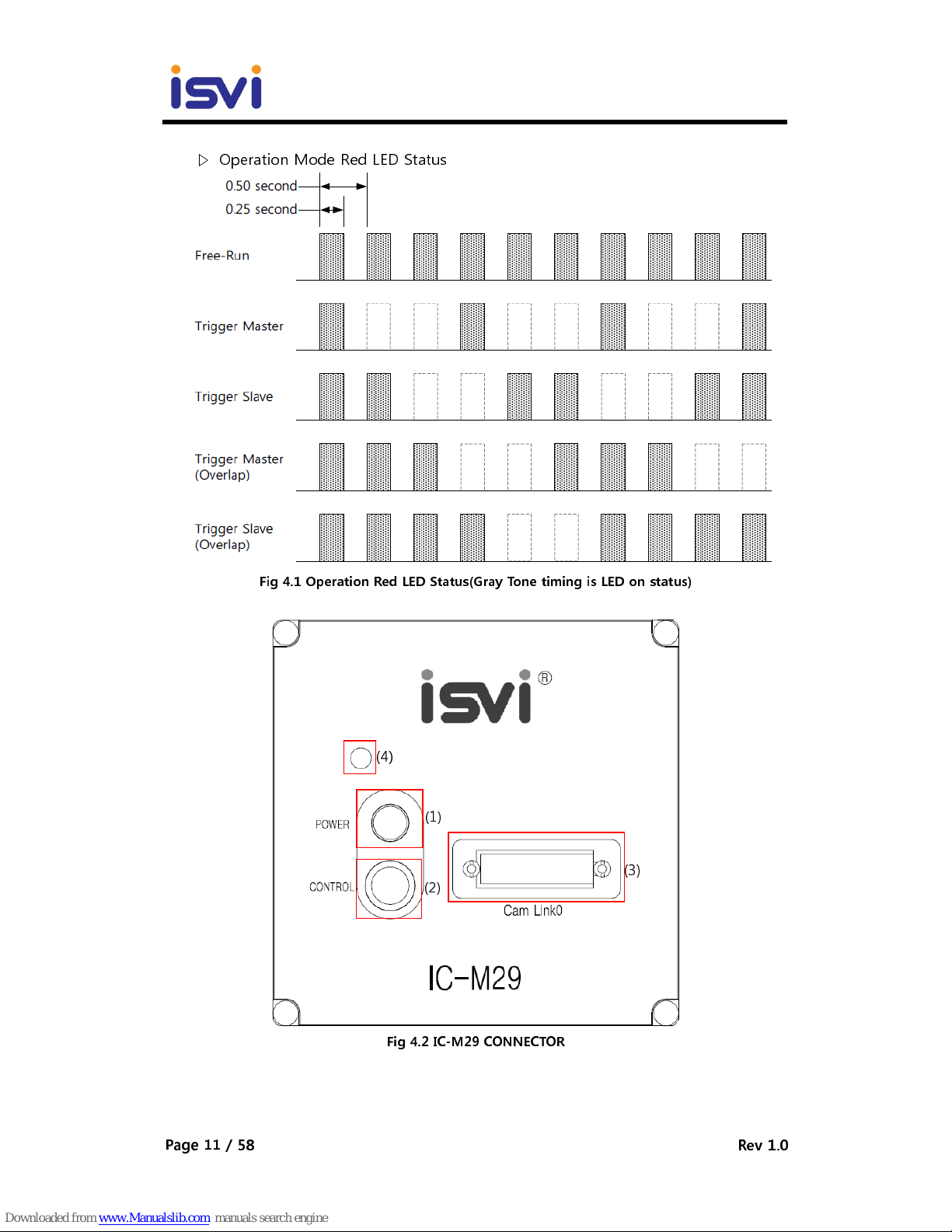
4.1 General Description
As shown in the following figure, 3 types of connectors and status indicator LED
Are located on the back of the camera and have the functions as follows :
(1) Power Connector : 6 pin Power Input
▷ Camera Power Input(DC-12V/15W)
(2) Control Connector : 12 pin Control Connector
▷ External Trigger Signal Input(2 Pin) and Strobe Output(1 Pin)
▷ Firmware Download Input(9 Pin)
(3) 26 pin Camera-Link Connector
▷ Video Data Transmission, Camera Control
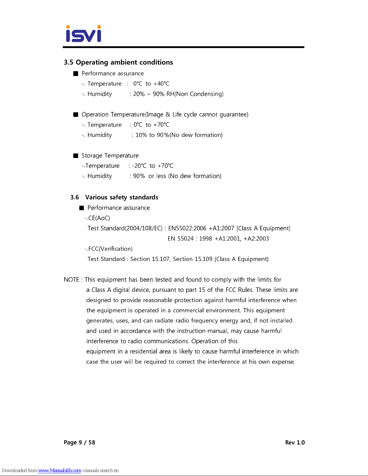
(4) Status LED
▷ Initial Status Red LED Sequence
1) Red LED on 0.7 second : Camera operates in power on
2) Red LED off 8.3 second : Initial Status
3) Red LED flashing at 0.5 second intervals : Camera Freerun operation
IC-M29
Page 11 / 58
Rev 1.0
▷ Operation Mode Red LED Status
Fig 4.1 Operation Red LED Status(Gray Tone timing is LED on status)
Fig 4.2 IC-M29 CONNECTOR
(1)
(2)
(3)
(4)
IC-M29
Page 12 / 58
Rev 1.0
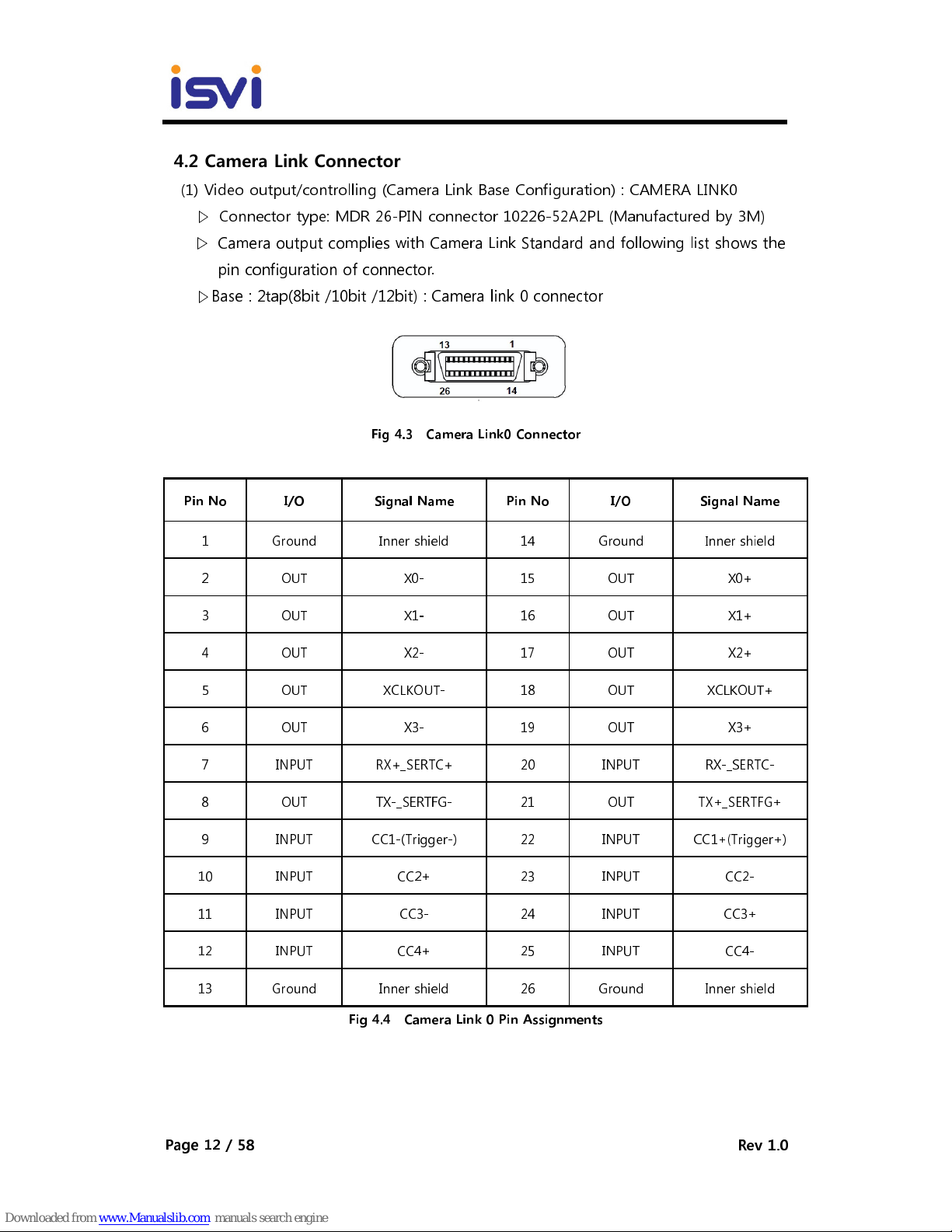
4.2 Camera Link Connector
(1) Video output/controlling (Camera Link Base Configuration) : CAMERA LINK0
▷ Connector type: MDR 26-PIN connector 10226-52A2PL (Manufactured by 3M)
▷ Camera output complies with Camera Link Standard and following list shows the
pin configuration of connector.
▷Base : 2tap(8bit /10bit /12bit) : Camera link 0 connector
Fig 4.3 Camera Link0 Connector
Fig 4.4 Camera Link 0 Pin Assignments
Pin No I/O Signal Name Pin No I/O Signal Name
1 Ground Inner shield 14 Ground Inner shield
2 OUT X0- 15 OUT X0+
3 OUT X1- 16 OUT X1+
4 OUT X2- 17 OUT X2+
5 OUT XCLKOUT- 18 OUT XCLKOUT+
6 OUT X3- 19 OUT X3+
7 INPUT RX+_SERTC+ 20 INPUT RX-_SERTC-
8 OUT TX-_SERTFG- 21 OUT TX+_SERTFG+
9 INPUT CC1-(Trigger-) 22 INPUT CC1+(Trigger+)
10 INPUT CC2+ 23 INPUT CC2-
11 INPUT CC3- 24 INPUT CC3+
12 INPUT CC4+ 25 INPUT CC4-
13 Ground Inner shield 26 Ground Inner shield
IC-M29
Page 13 / 58
Rev 1.0
4.3 Camera Link Interface
The video output is Camera Link, where the 8 channels with 8bit video are placed in
a base configuration. The digital output signals follow the Camera Link standardized
multiplexed signal output interface.
The output driver is NS type DS90CR287, and the receiver is NS type DS90CR288. The
data bits from the digital video, FVAL, LVAL and DVAL are multiplexed into the twisted
pairs, which are a part of the Camera Link. Trigger signals and the serial camera control
are feed directly through its own pairs.
The 26 pin connector pin assignment follows the Camera Link base configuration. For a
detailed description of Camera Link specifications, please refer to the Camera Link
standard specifications found on http://www.machinevisiononline.org
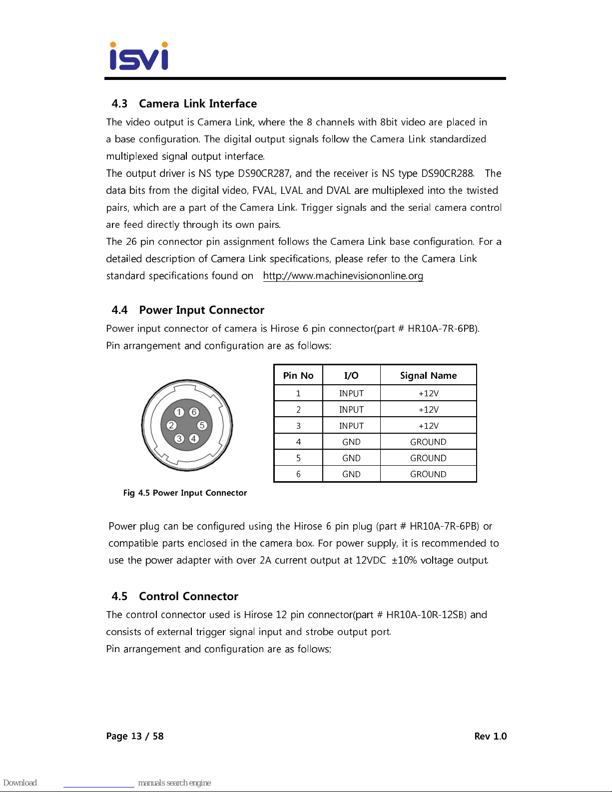
4.4 Power Input Connector
Power input connector of camera is Hirose 6 pin connector(part # HR10A-7R-6PB).
Pin arrangement and configuration are as follows:
Fig 4.5 Power Input Connector
Power plug can be configured using the Hirose 6 pin plug (part # HR10A-7R-6PB) or
compatible parts enclosed in the camera box. For power supply, it is recommended to
use the power adapter with over 2A current output at 12VDC ±10% voltage output.
4.5 Control Connector
The control connector used is Hirose 12 pin connector(part # HR10A-10R-12SB) and
consists of external trigger signal input and strobe output port.
Pin arrangement and configuration are as follows:
Pin No I/O Signal Name
1 INPUT +12V
2 INPUT +12V
3 INPUT +12V
4 GND GROUND
5 GND GROUND
6 GND GROUND

IC-M29
Page 14 / 58
Rev 1.0
Fig 4.6 I/O Control Connector
▷ Camera firmware upgrade
Camera firmware upgrade is available through the ISVI firmware cable.
Fig 4.7 ISVI Firmware cable
4.6 Trigger Input Circuit
Following figure shows trigger signal input circuit of 12 pin connector. Trigger signal
entered is delivered to internal circuit through photo coupler. Minimum trigger width
that can be recognized at camera is 100us. If trigger signal entered is less than 100us,
trigger signal is ignored in camera. External trigger signal can approve signals to the
circuits in the 2 methods shown below.
Fig 4.8 Trigger Input Schematic
Pin I/O Signal Name
Pin
I/O Signal Name
1 INPUT Trigger + 7 OUTPUT Reserved
2 INPUT Trigger - 8 INPUT Reserved
3 OUTPUT Strobe Output 9 INPUT Reserved
4 INPUT Reserved 10 OUTPUT Reserved
5
GND GROUND 11 INPUT Reserved
6 INPUT Reserved 12 INPUT Reserved
IC-M29
Page 15 / 58
Rev 1.0
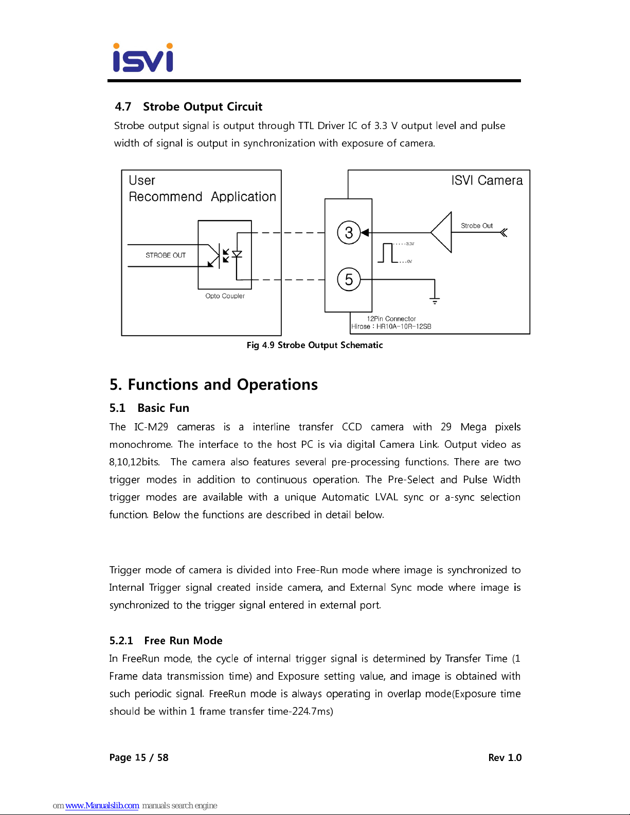
4.7 Strobe Output Circuit
Strobe output signal is output through TTL Driver IC of 3.3 V output level and pulse
width of signal is output in synchronization with exposure of camera.
Fig 4.9 Strobe Output Schematic
5. Functions and Operations
5.1 Basic Functions
The IC-M29 cameras is a interline transfer CCD camera with 29 Mega pixels
monochrome. The interface to the host PC is via digital Camera Link. Output video as
8,10,12bits. The camera also features several pre-processing functions. There are two
trigger modes in addition to continuous operation. The Pre-Select and Pulse Width
trigger modes are available with a unique Automatic LVAL sync or a-sync selection
function. Below the functions are described in detail below.
5.2 Trigger operation
Trigger mode of camera is divided into Free-Run mode where image is synchronized to
Internal Trigger signal created inside camera, and External Sync mode where image is
synchronized to the trigger signal entered in external port.
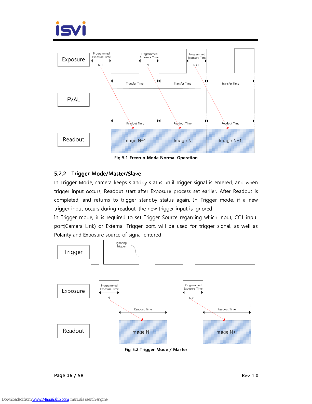
5.2.1 Free Run Mode
In FreeRun mode, the cycle of internal trigger signal is determined by Transfer Time (1
Frame data transmission time) and Exposure setting value, and image is obtained with
such periodic signal. FreeRun mode is always operating in overlap mode(Exposure time
should be within 1 frame transfer time-224.7ms)
IC-M29
Page 16 / 58
Rev 1.0
Fig 5.1 Freerun Mode Normal Operation
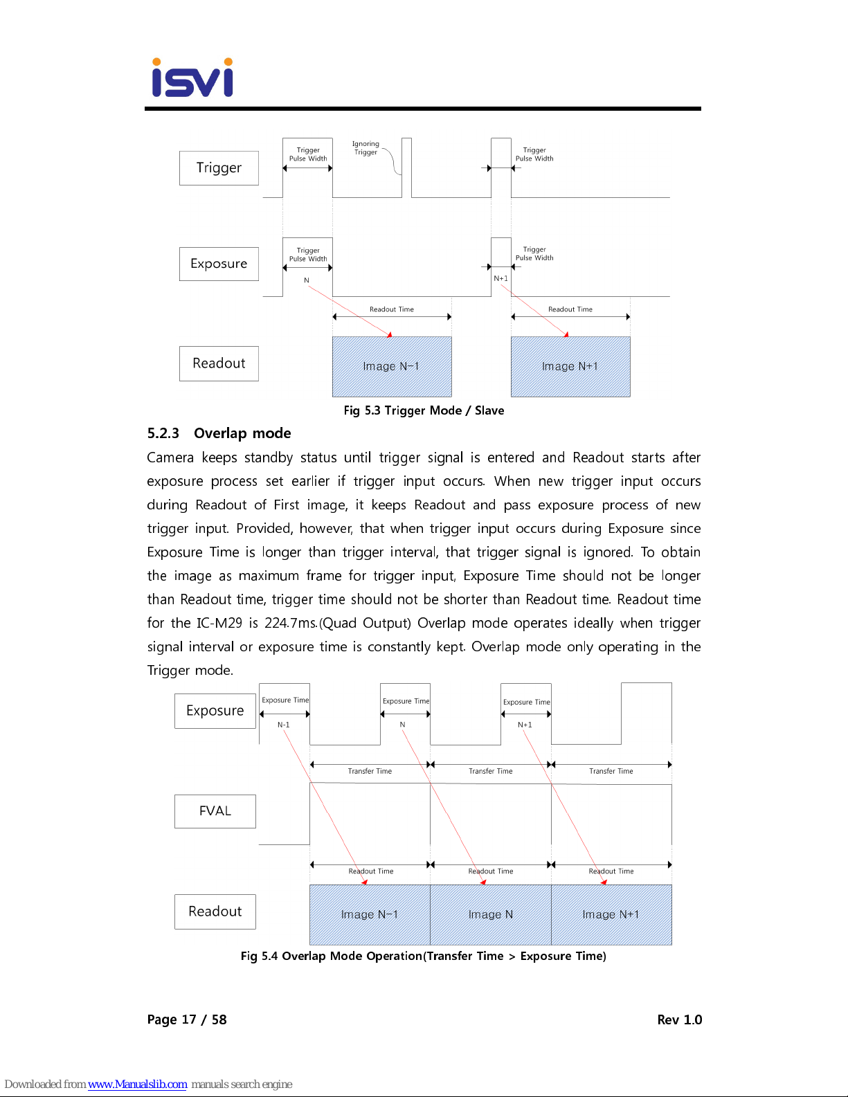
5.2.2 Trigger Mode/Master/Slave
In Trigger Mode, camera keeps standby status until trigger signal is entered, and when
trigger input occurs, Readout start after Exposure process set earlier. After Readout is
completed, and returns to trigger standby status again. In Trigger mode, if a new
trigger input occurs during readout, the new trigger input is ignored.
In Trigger mode, it is required to set Trigger Source regarding which input, CC1 input
port(Camera Link) or External Trigger port, will be used for trigger signal, as well as
Polarity and Exposure source of signal entered.
Fig 5.2 Trigger Mode / Master
IC-M29
Page 17 / 58
Rev 1.0
Fig 5.3 Trigger Mode / Slave
5.2.3 Overlap mode
Camera keeps standby status until trigger signal is entered and Readout starts after
exposure process set earlier if trigger input occurs. When new trigger input occurs
during Readout of First image, it keeps Readout and pass exposure process of new
trigger input. Provided, however, that when trigger input occurs during Exposure since
Exposure Time is longer than trigger interval, that trigger signal is ignored. To obtain
the image as maximum frame for trigger input, Exposure Time should not be longer
than Readout time, trigger time should not be shorter than Readout time. Readout time
for the IC-M29 is 224.7ms.(Quad Output) Overlap mode operates ideally when trigger
signal interval or exposure time is constantly kept. Overlap mode only operating in the
Trigger mode.
Fig 5.4 Overlap Mode Operation(Transfer Time > Exposure Time)
IC-M29
Page 18 / 58
Rev 1.0
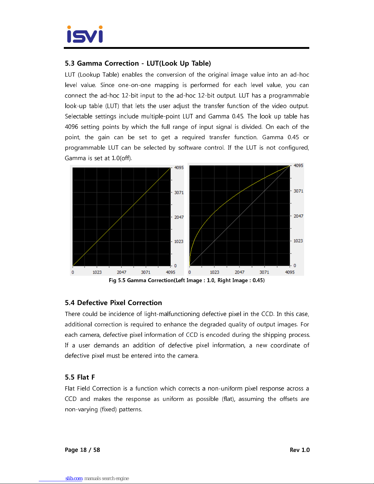
5.3 Gamma Correction - LUT(Look Up Table)
LUT (Lookup Table) enables the conversion of the original image value into an ad-hoc
level value. Since one-on-one mapping is performed for each level value, you can
connect the ad-hoc 12-bit input to the ad-hoc 12-bit output. LUT has a programmable
look-up table (LUT) that lets the user adjust the transfer function of the video output.
Selectable settings include multiple-point LUT and Gamma 0.45. The look up table has
4096 setting points by which the full range of input signal is divided. On each of the
point, the gain can be set to get a required transfer function. Gamma 0.45 or
programmable LUT can be selected by software control. If the LUT is not configured,
Gamma is set at 1.0(off).
Fig 5.5 Gamma Correction(Left Image : 1.0, Right Image : 0.45)
5.4 Defective Pixel Correction
There could be incidence of light-malfunctioning defective pixel in the CCD. In this case,
additional correction is required to enhance the degraded quality of output images. For
each camera, defective pixel information of CCD is encoded during the shipping process.
If a user demands an addition of defective pixel information, a new coordinate of
defective pixel must be entered into the camera.
5.5 Flat Field Correction
Flat Field Correction is a function which corrects a non-uniform pixel response across a
CCD and makes the response as uniform as possible (flat), assuming the offsets are
non-varying (fixed) patterns.
 Loading...