

ISSI IS32LT3120 Demo Manual
IS32LT3120 Dual Channel Linear LED Driver With Fade In/Fade Out
DESCRIPTION
The IS32LT3120 is a linear programmable current
regulator consisting of 2 output channels capable of up
to 200mA each. Each channel features an ON/OFF
input pin to toggle the channel between the OFF
condition and the source condition.
The device integrates 63 steps fade in and fade out
algorithm (Gamma correction) which causes the output
LED current to gradually ramp up to the full source
value after the channel’s control pin is pulsed. The
same controller causes the LED current to gradually
ramp down to zero if the channel’s input control pin is
pulsed while the output channel is on.
FEATURES
Dual output channels source up to 200mA each
Independent debounced ON/OFF control for each
channel
Programmable current via a single external
resistor
Programmable fade in, fade out via external
resistor
- Pull down resistor value sets fade speed
- Gamma corrected fade in/out algorithm
Fault Protection:
- LED string shorted to GND
- Over temperature
SOP-8-EP packages
Automotive Grade - AEC-Q100 (pending)
Operating temperature range from -40°C ~ +125°C
QUICK STAR T
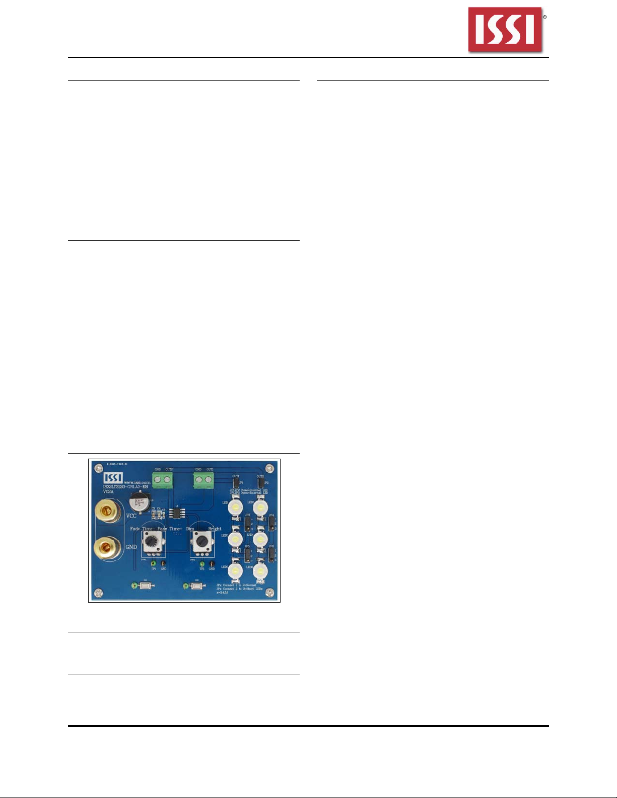
Figure 1: Photo of IS32LT3120 Evaluation Board
RECOMMENDED EQUIPMENT
12V,1A DC power supply
ABSOLUTE MAXIMUM RATINGS
≤ 45V power supply
Caution: Do not exceed the conditions listed above, otherwise
the board will be damaged.
PROCEDURE
The IS32LT3120 evaluation board is fully assembled
and tested. Follow the steps listed below to verify
board operation.
Caution: Do not turn on the power supply until all connections
are completed.
1) Connect the ground terminal of the power supply
to the GND and the positive terminal to the VCC.
The VCC supply should be set close to the
NOTE:
IS32LT3120 minimal headroom voltage of 0.5V
(Vcc – Voutx) for best thermal performance. The
board can be operated with a larger headroom
voltage as long as the increase in package
temperature is monitored. Exceeding the device
package temperature specification will cause the
device to enter thermal protection mode.
2) The fade time of both channels is adjusted by the
variable resistor (RW1).Turn RW1 counter
clockwise to decrease fade time, and clockwise to
increase fade time. Once the desired fade time is
set, measure the resistor value across TP1 and
GND. Use this measured resistor value to replace
the variable resistor RW1 and R3 (see schematic
Figure 2).
3) The output current of both channels (OUT1 and
OUT2) is adjusted by the variable resistor (RW2).
Turn RW2 counter clockwise to decrease the
output current of both channels, and clockwise to
increase the output current of both channels. The
test point TP2 can be used to detect the resistor
value at the ISET pin. The final resistance can be
measured with an ohm meter across TP2 and
GND pins. Use this measured resistor value to
replace the variable resistor RW2 and R4 (see
schematic Figure 2).
4) Momentary contact buttons (K1, K2) are used to
individually enable/disable the Outx LED channels.
Press K1 to enable the onboard LED string for
channel 1. Press K2 to enable the onboard LED
string for channel 2. In both cases wait for the
LED string to be fully ON (fade time completed)
before pressing the button (K1 or K2) to turn OFF
the corresponding LED string. Always wait for
completion of fade time before pressing either K1
or K2.
5) JP1is used to connect the IS32LT3120 Out 1 (pin
4) to the onboard LED string (LED1, LED3 and
LED5). JP2 connects the device Out2 (pin 5) to
the onboard LED string (LED2, LED4, LED6). Use
one of the green terminal blocks to connect an
external LED string. Remove the corresponding
jumper header (JP1 or JP2) to disable the
onboard LED string. Note: Connecting an
external LED string without removing the onboard
string jumper header will drive both onboard and
external LED strings in parallel resulting in lower
current drive to both strings.
Integrated Silicon Solution, Inc. – www.issi.com 1
Rev.A, 08/11/2014
IS32LT3120 Dual Channel Linear LED Driver With Fade In/Fade Out
6) The on board LED string size can be adjusted
from 1 to 3 LEDs by using jumper headers
JP3~JP6. Connecting the header to pins 2-3
disables the corresponding LED, ie JP3 pins 2-3
disables LED3. To enable all the LED3~LED6
connect JP3~JP6 to pins 1-2.
.
ORDERING INFORMATION
Part No. Temperature Range Package
IS32LT3120-GRLA3-EB -40°C ~ +125°C (Automotive) SOP-8-EP, Lead-free
Table1: Ordering Information
For pricing, delivery, and ordering information, please contact ISSI’s analog marketing team at
analog@issi.com
or (408) 969-6600
EVALUATION BOARD OPERATION
IS32LT3120 evaluation board drives two strings of
WLEDs. There are two variable resistors used for
adjusting the fade time (RW1), LED current (RW2).
SETTING THE FADE TIME
The fade time, either in or out, for both channels is the
same, and is set by a single external programming
resistor (R
). The fade time is programmable by
TSET
Equation (1):
The device is protected from an output over current
condition caused by an accidental short circuit of the
ISET pin, by internally limiting the maximum current in
the event of an ISET short circuit to 260mA.
THERMAL ROLLOFF
The output current of both channels will be equal to the
set value so long as the die temperature of the IC
remains below 125°C (Typical). If the die temperature
exceeds this threshold, the output current of the device
sRt
TSET
For example, R
Note: In order to get the optimized effect, the recommended
fading time is between 1.5s (RTSET=600kΩ) and 0.25s
(RTSET=100kΩ).
=100kΩ, fade time is about 0.25s.
TSET
5.2 (1)
If the TSET pin is tied directly to GND, the fade in/out
function is canceled and the ramp time is about 73µs,
or ‘instant on’. However, the debounce feature of the
ENx pin is not disabled.
OUTPUT CURRENT SETTING
A single programming resistor (R
) controls the
ISET
maximum output current for both output channels
simultaneously. The programming resistor may be
computed using the following Equation:
will begin to reduce at a rate of 3%/°C.
The roll off slope is related to ISET value. When
I
=20mA, the roll off slope is about 3.7%. When
SET
I
=200mA, the roll off slope is about 2.2%
SET
FAULT DETECTION
An output shorted to GND fault is detected if the output
voltage on a channel drops below the low voltage
threshold V
and remains below the threshold for tFD.
SCD
The channel (OUTx) with the short condition will
reduce its output current to 20% of I
SET
.
When short condition is removed, output current will
recover to original value.
When output current is larger than limit value, about
260mA, the output current will be clamped. When the
2000
R
ISET
I
(10kΩ≤R
SET
≤100kΩ)
ISET
open fault condition is recovered, there will be a large
current pulse about 10µs.
Integrated Silicon Solution, Inc. – www.issi.com 2
Rev.A, 08/11/2014
 Loading...