

ISSI IS31LT3360, IS31LT3360-SDLS3-EB3CH, IS31LT3360 series, IS31LT3360-SDLS4-EB3CH User Manual
IS31LT3360 3CH DEMO BOARD GUIDE
Integrated Silicon Solution, Inc. – www.issi.com
Rev. B, 04/27/2016
1
DESCRIPTION
The IS31LT3360 is a continuous mode inductive
step-down converter, designed for driving a single LED
or multiple series connected LEDs efficiently from a
voltage source higher than the LED voltage. The chip
operates from an input supply between 6V and 40V
and provides an externally adjustable output current of
up to 1.2A.
The IS31LT3360 includes an integrated output switch
and a high-side output current sensing circuit, which
uses an external resistor to set the nominal average
output current.
Output current can be adjusted linearly by applying an
external control signal to the ADJ pin. The ADJ pin will
accept either a DC voltage or a PWM waveform. This
will provide either a continuous or a gated output
current.
Applying a voltage of 0.2V or lower to the ADJ pin
turns the output off and switches the chip into a low
current standby state.
The chip is assembled in SOT89-5 package.
IS31LT3360 3CH DEMO board is used in RGB lamp or
the general LED lamp.
FEATURES
Simple low parts count
Internal 40V power switch
Wide input voltage range: 6V to 40V
Up to 1.2A output current
High efficiency (up to 98% )
Typical 1200:1 dimming rate
Typical 3% output current accuracy
Single pin on/off and brightness control using DC
voltage or PWM
Up to 1MHz switching frequency
Inherent open-circuit LED protection
Thermal shutdown protection circuitry
QUICK START
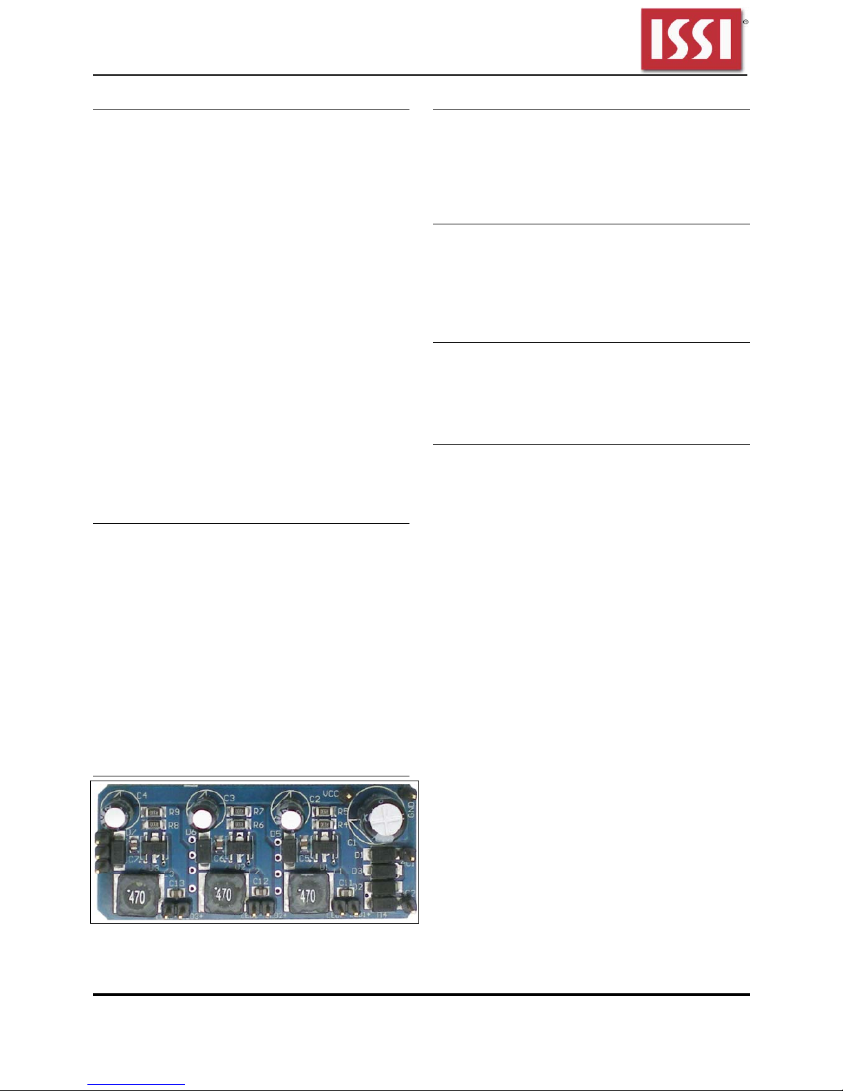
Figure 1: Photo of IS31LT3360-3CH Evaluation Board
RECOMMENDED EQUIPMENT
40VDC power supply
3 pcs of LED panel (3 WLEDs, 10 LEDs in series
on each panel)
Multi-meter
RECOMMENDED INPUT AND OUTPUT RATINGS
Input: 6~40VDC
Output: 1~10 LEDs in series/667mA
Note: The input voltage must be 2V higher than the output
voltage (total V
F
).
ABSOLUTE MAXIMUM RATINGS
Input voltage ≤ 40VDC
Caution: Do not exceed the conditions listed above, otherwise
the board will be damaged.
PROCEDURE
The IS31LT3360 DEMO Board is fully assembled and
tested. Follow the steps listed below to verify board
operation.
Caution: Do not turn on the power supply until all connections
are completed.
1) Connect the terminals of the power supply to the
AC1 and AC2 pin(If the board don’t have the
rectifier(D1-D4), Connect the positive terminal of
the power supply to the VCC of the board and the
negative terminal of power supply to the GND of
the board) .
2) Connect the negative of the one of LED panel
(LED arrays) to the LED1- terminal. And connect
the positive of the same LED panel (LED arrays)
to the LED1+ terminal.
3) Connect the other two LED panels to LED2 and
LED3 as above.
4) Turn on the power supply and the LED panels
(LED arrays) will be light.
IS31LT3360 3CH DEMO BOARD GUIDE
Integrated Silicon Solution, Inc. – www.issi.com
Rev. B, 04/27/2016
2
ORDER INFORMATION
Part No. Temperature Range Package
IS31LT3360-SDLS3-EB3CH
IS31LT3360-SDLS4-EB3CH
-40°C to +105°C (Industrial)
-40°C to +125°C (Industrial)
SOT89-5, Lead-free
For pricing, delivery, and ordering information, please contacts ISSI’s analog marketing team at
analog@issi.com or (408) 969-6600.
DETAILED DESCRIPTION
LED Current Control
The nominal average output current in the LED(s) is
determined by the value of the external current sense
resistor (R
S
) connected between VIN and I
SENSE
and in
is given by:
I
OUT_NOM
= 0.1/Rs [for Rs>0.082Ω]
The table below gives values of nominal average
output current for several preferred values of current
setting resistor (Rs) in the typical application circuit
shown on Page 1:
R
S
(Ω)
Nominal Average Output
Current (mA)
0.082 1200
0.1 1000
0.15 667
0.3 333
V
SENSE
is divided into two ranges to improve current
accuracy, please refer to bin information on Page 3.
The above values assume that the ADJ pin is floating
and at a nominal voltage of V
REF
=1.2V.
Note that R
S
=0.082Ω is the minimum allowed value of
sense resistor under these conditions to maintain
switch current below the specified maximum value.
It is possible to use different values of R
S
if the ADJ pin
is driven from an external voltage.
Inductor selection
Recommended inductor values are in the range 47μH
to 220μH.
Higher values of inductance are recommended at
higher supply voltages and low output current in order
to minimize errors due to switching delays, which
result in increased ripple and lower efficiency. Higher
values of inductance also result in a smaller change in
output current over the supply voltage range. The
inductor should be mounted as close to LX pin as
possible with low resistance connections to LX and V
IN
pins.
PCB LAYOUT CONSIDERATION
Decoupling Capacitors And Coil
It is particularly important to mount the coil and the
input decoupling capacitor close to the chip to
minimize parasitic resistance and inductance, which
will degrade efficiency. The input decoupling capacitor
(0.1µF fixed) must be placed as close to the V
IN
and
GND pins as possible. It is also important to take
account of any trace resistance in series with current
sense resistor R
S
.
LX Pin
The LX pin of the chip is a fast switching node, so PCB
traces should be kept as short as possible. To
minimize ground 'bounce', the ground pin of the chip
should be soldered directly to the ground plane.
ADJ Pin
The ADJ pin is a high impedance input, so when left
floating, PCB traces to this pin should be as short as
possible to reduce noise pickup. ADJ pin can also be
connected to a voltage between 1.2V~5V. In this case,
the internal circuit will clamp the output current at the
value which is set by V
ADJ
=1.2V.
High Voltage Traces
Avoid running any high voltage traces close to the ADJ
pin, to reduce the risk of leakage due to board
contamination. Any such leakage may raise the ADJ
pin voltage and cause excessive output current. A
ground ring placed around the ADJ pin will minimize
changes in output current under these conditions.
 Loading...