

Page 1
IS31IO7326 Debounced 8x8 Key-Scan Controller Evaluation Board Guide
Description
IS31IO7326 is a 64 key, key-scan controller. It offloads
the burden of keyboard scanning from the host
processor. The IS31IO7326 supports keypad matrix of
up to 8×8. Key press and release events are encoded
into a byte format and loaded into a key event register
for retrieval by the host processor.
To minimize power, the IS31IO7326 automatically
enters a low power standby mode when there is no
keypad, I/O, or host activity.
Features
• Supply voltage range from 3.0V to 5.5V
• 400kHz I2C serial interface
• Available for multi-key press detect
• Low 0.3µA (typ.) standby current
• Operate in -40°C to +125°C
• Pb-free 4mm × 4mm QFN-24 package
Quick Start
Recommended Equipment
• 5.0V, 2A power supply
Absolute Maximum Ratings
• ≤ 5.5V power supply
Caution: Do not exceed the conditions listed above, otherwise
the board will be damaged.
Procedure
The IS31FL7326 evaluation board is fully assembled
and tested. Follow the steps listed below to verify
board operation.
Caution: Do not turn on the power supply until all connections
are completed.
1) Connect the ground terminal of the power supply
to the GND and the positive terminal to the VCC.
Or connect the DC power to the connector (DC
IN).
2) Turn on the power supply and pay attention to the
supply current. If the current exceeds 200mA,
please check for circuit fault.
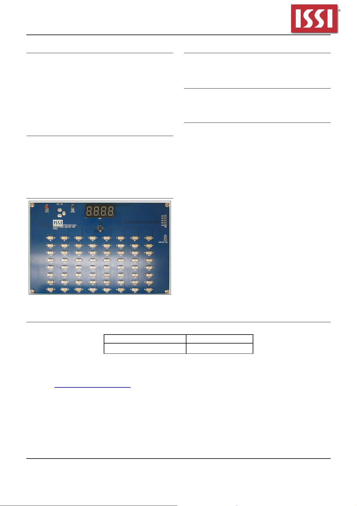
Figure 1: Photo of IS31IO7326 Evaluation Board
Evaluation Board Ordering Information
Part No. IC Package
IS31IO7326-QFLS4-EB QFN-24, Lead-free
Table1: Ordering Information
For pricing, delivery, and ordering information, please contacts ISSI’s analog marketing
team at analog_mkt@issi.com or (408) 969-6600.
Integrated Silicon Solution, Inc. – www.issi.com
R1.0, 08/23/2012
1
Page 2
IS31IO7326 Debounced 8x8 Key-Scan Controller Evaluation Board Guide
Evaluation Board Operation
K0 to K63 are push buttons on the demo
board. When each of the button is pressed
briefly, a number corresponding to the key will
be displayed. When the button is pressed
and held for a few seconds, the period dot will
also be displayed. If two buttons are
pressed at the same time, the corresponding
key numbers will be displayed.
Note:
IS31IO7326 solely controls the Key-Scan function on the
evaluation board.
PP0
PP1
PP2
PP3
PP4
PP5
PP6
PP7
3V
R4
4.7K
SCL
SDA
INT
RST
Integrated Silicon Solution, Inc. – www.issi.com
R1.0, 08/23/2012
VCC
R5
K0 K8 K16 K24 K32
100K
K1 K9 K17 K25 K33 K41 K49 K57
K2 K10 K18 K26 K34 K42 K50 K58
K3 K11 K19 K27 K35 K43 K51 K59
K4 K12 K20 K28 K36 K44 K52 K60
K5 K13 K21 K29 K37 K45 K53 K61
K6 K14 K22 K30 K38 K46 K54 K62
K7 K15 K23 K31 K39 K47 K55 K63
OD0 OD1 OD2 OD3 OD4 OD5 OD6 OD7
U1
VCC
21
VCC
C2
1uF
R1
R2
4.7K
4.7K
19
SCL
20
SDA
22
INT
23
RST
R3
100K
18
AD0
24
AD1
9
GND
IS31IO7326
R6
100K
R7
100K
1
PP0
2
PP1
3
PP2
4
PP3
14
PP4
15
PP5
16
PP6
17
PP7
5
OD0
6
OD1
7
OD2
8
OD3
10
OD4
11
OD5
12
OD6
13
OD7
R8
100K
PP0
PP1
PP2
PP3
JP1
PP4
OPEN=EXT CTRL
PP5
PP6
PP7
OD0
OD1
OD2
OD3
OD4
OD5
OD6
OD7
TP3
R9
100K
U3
1
20
19
18
14
10
8
3
2
LPC922
GND
5
RST
4
SDA
3
SCL
2
INT
1
P0.0/CMP2/KBI0
P0.1/CIN2B/KBI1
P0.2/CIN2A/KBI2
P0.3/CIN1B/KBI3
P0.6/CMP1/KBI6
P1.2/T0/SCL
P1.4/INT1
P1.6
P1.7
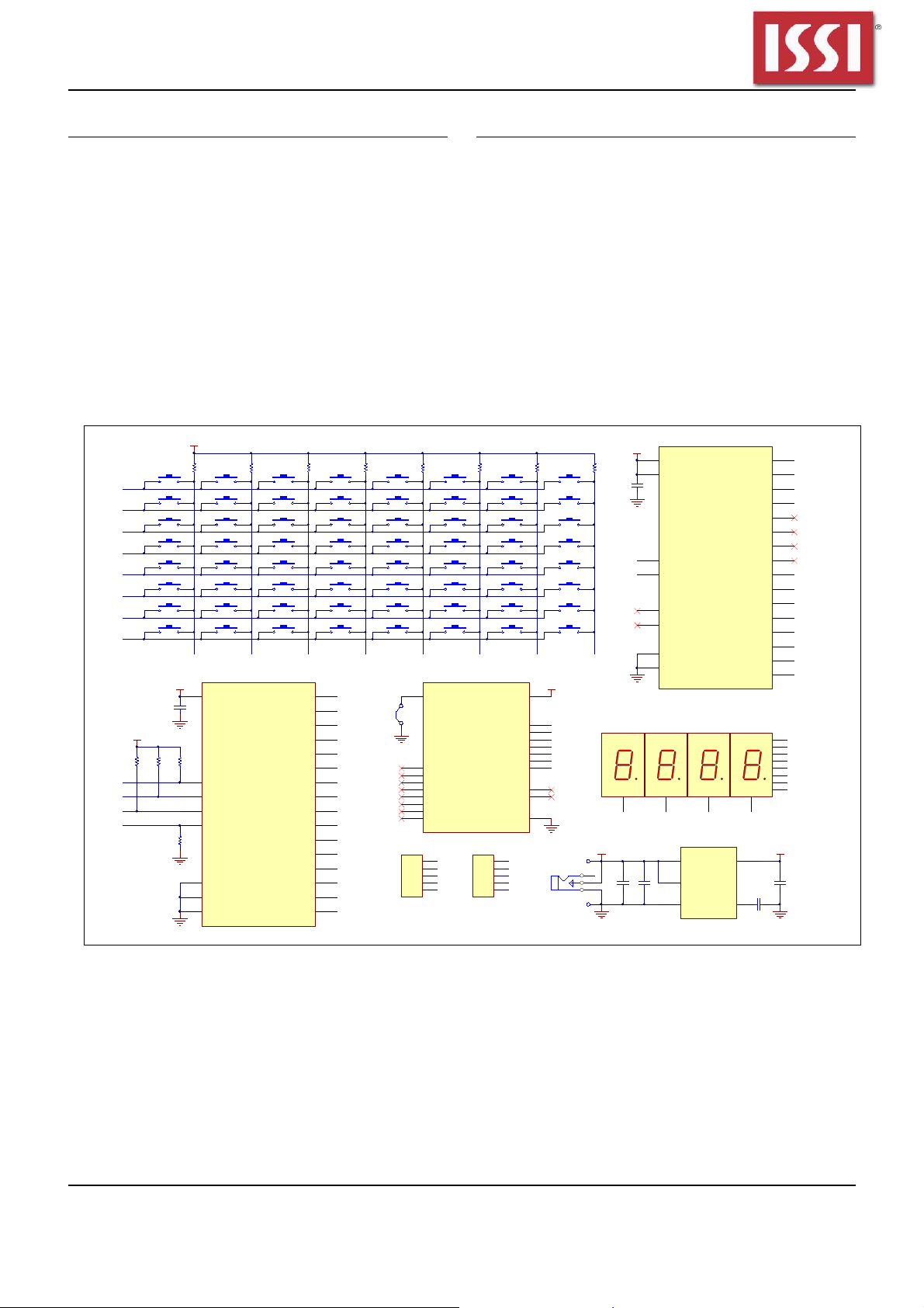
Figure 2:IS31IO7326 Application Schematic
2
Software support
Note:
JP1 is set to close circuit by default. If it is set to open, the
on-board MCU will stop working. The pins driving the I2C pin
from MCU will be set to High Impedance. External control
signals can be connected to TP3 port to control the IS31IO7326.
Refer to the datasheet to get more information about
IS31IO7326.
U4
VCC
11
R10
K40 K48 K56
100K
P0.4/CIN1A/KBI4
P0.5/CMPREF/KBI5
P0.7/T1/KBI7
P1.3/INT0/SDA
P3.1/XTAL1
P3.0XTAL2/CLKOUT
TP4
5
4
3
2
1
P1.0/TXD
P1.1/RXD
P1.5/RST
3V
P0.5
P0.4
RESET
GND
VDD
R11
100K
3V
15
17
P0.4
16
P0.5
13
RST
12
SDA
11
SCL
9
INT
4
RESET
6
7
5
VSS
CON1
DC IN
R12
100K
TP1
10uFC11uF
TP2
VDD
3
SDB
C3
1uF
SDA
1
SDA
SCL
2
SCL
4
IN
5
C_FILT
6
AD
20
GND
IS31FL3728
DIG1
H3
H2
H1
12
C4
8
9
U2
1
VDD
3
SD
2
GND
PAM3101
VOUT
C1
C2
C3
C4
C5
C6
C7
C8
R8/C9
R7/C10
R6/C11
R5
R4
R3
R2
R1
DP
g
f
e
d
c
b
a
H4
6
C1C2C3C4
3VVCC
5
C5
10nF
4
BP
24
C1
23
C2
22
C3
21
C4
19
18
17
16
15
DP
14
g
13
f
12
e
10
d
9
c
8
b
7
a
3
DP
5
g
10
f
1
e
2
d
4
c
7
b
11
a
C6
1uF
Page 3

IS31IO7326 Debounced 8x8 Key-Scan Controller Evaluation Board Guide
Bill of Materials
Name Symbol Description Qty Supplier Part No.
I/O IC U1 16 I/O ports.Expander 1 ISSI IS31IO7326
LDO U2 Low-dropout Regulator 1 PAM PAM3101
MCU U3 Microcontroller 1 NXP LPC922
LED Driver U4 Array FxLED Driver 1 ISSI IS31FL3728
Displayer DIG1
Resistors R1,R2,R4 RES,4.7k,1/16W,±5%,SMD 3
Resistor R3 RES,100k,1/16W,±5%,SMD 1
Resistors R5~R12 RES,100k,1/16W,±5%,SMD 8
Capacitor C1 CAP,10µF,16V,±20%,SMD 1
Capacitors C2,C3,C4,C6 CAP, 1µF,16V,±20%,SMD 4
Capacitor C5 CAP,10nF,16V,±20%,SMD 1
4 Digit Display, Common
Kathode
1 ZSO 3461AS
Buttons K0~K63 Button SMD 64
Table 2: Bill of Materials, refer to Figure 2 above.
Integrated Silicon Solution, Inc. – www.issi.com
R1.0, 08/23/2012
3
Page 4

IS31IO7326 Debounced 8x8 Key-Scan Controller Evaluation Board Guide
10
11
2
1
0
2
2
2
1
2
000000
43
2
5
6
7
8
9
10
000000
21
20
19
18
22
1312
11
10
11 12
17
9
13
14
1516
14
12
00
1
2
3
4
5
1
2
0
Figure 3: Board Component Placement Guide -Top Layer
Figure 4: Board PCB Layout- Top Layer
Integrated Silicon Solution, Inc. – www.issi.com
R1.0, 08/23/2012
4
Page 5

IS31IO7326 Debounced 8x8 Key-Scan Controller Evaluation Board Guide
10
11
2
1
0
2
2
2
1
2
000000
43
2
5
6
7
8
9
10
000000
21
20
19
18
22
1312
11
10 11 12
17
9
13
14
1516
14
12
00
1
2
3
4
5
1
2
0
Figure 5: Board Component Placement Guide -Bottom Layer
Figure 6: Board PCB Layout-Bottom Layer
Integrated Silicon Solution, Inc. – www.issi.com
R1.0, 08/23/2012
5
Page 6

IS31IO7326 Debounced 8x8 Key-Scan Controller Evaluation Board Guide
Copyright © 201
2 Integrated Silicon Solution, Inc. All rights reserved. ISSI reserves the right to make changes to this specification
and its products at any time without notice. ISSI assumes no liability arising out of the application or use of any information,
products or services described herein. Customers are advised to obtain the latest version of this device specification before relying
on any published information and before placing orders for products.
Integrated Silicon Solution, Inc. does not recommend the use of any of its products in life support applications where the failure or
malfunction of the product can reasonably be expected to cause failure of the life support system or to significantly affect its safety
or effectiveness. Products are not authorized for use in such applications unless Integrated Silicon Solution, Inc. receives written
assurance to its satisfaction, that:
a.) the risk of injury or damage has been minimized;
b.) the user assume all such risks; and
c.) potential liability of Integrated Silicon Solution, Inc is adequately protected under the circumstances
Integrated Silicon Solution, Inc. – www.issi.com
6
R1.0, 08/23/2012
 Loading...