

Page 1
IS31IO7325 Multi-Function I/O Driver Evaluation Board Guide
Description
The IS31IO7325 2-wire serial-interfaced peripheral
features 16 I/O ports. Ports are divided into eight push
pull I/Os and eight open-drain I/Os and transition
detection.
Any of the 16 I/O ports can be configured as an input
or an output. All I/O ports configured as inputs are
continuously monitored for state changes (transition
detection). State changes are indicated by the INT
output. The interrupt is latched, allowing detection of
transient changes. When the IS31IO7325 is
subsequently read through the serial interface, any
pending interrupt is cleared.
_______
Features
• Supply voltage range from 2.4V to 5.5V
• 400kHz I2C serial interface
• 8 push-pull I/O ports
• 8 open-drain I/O ports, rated to 20mA sink current
at 0.22V headroom
• Selectable I/O port power-up default logic states
_______
• INT
• Low 0.3µA (Typ.) standby current
• Pb-free SOP-24 package
output alerts change on inputs
Quick Start
Recommended Equipment
• 2.5V~5.5V, 2A power supply
Absolute Maximum Ratings
• ≤ 5.5V power supply
Caution: Do not exceed the conditions listed above, otherwise
the board will be damaged.
Procedure
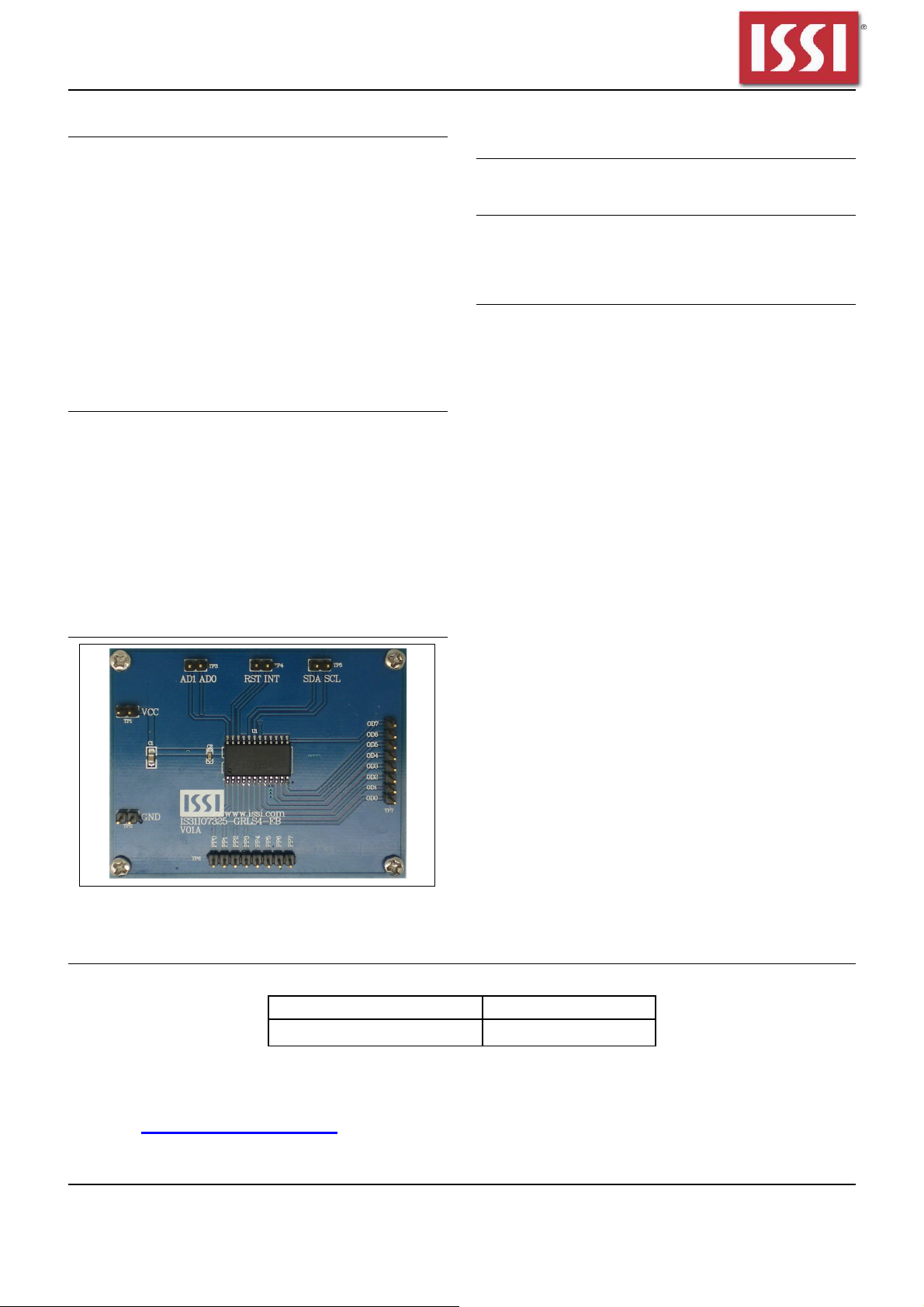
Follow the steps listed below operation.
1) Connect power positive terminal to VCC pin and
negative terminal to GND pin.
2) INT pin is pulled-up to VCC by a 4.7KΩ resistor.
3) SCL is an input clock pin. SDA is a bi-direction
open drain pin. Both of them are pulled-up to
VCC by 4.7KΩ resistors.
4) RST pin is Low active reset pin with 4.7KΩ
resistor pull-up.
5) AD1 and AD0 is used to set the I2C device
address. Their value can be 00, 01, 10 and 11 (0
is GND; 1 is VCC). After power-on, I/O output
will be dependent on the AD1 and AD0
connection (see Table 2 for details). Both AD1
and AD0 are pull-ed to GND by 100KΩ on this
demo board.
6) TP6 is PP output port while TP7 is OD output
port.
Figure 1: Photo of IS31IO7325 Evaluation Board
Evaluation Board Ordering Information
Part No. IC Package
IS31IO7325-GRLS4-TR SOP-24, Lead-free
Table1: Ordering Information
For pricing, delivery, and ordering information, please contacts ISSI’s analog marketing
team at analog_mkt@issi.com or (408) 969-6600.
Integrated Silicon Solution, Inc. – www.issi.com
R1.0, 08/13/2012
1
Page 2
IS31IO7325 Multi-Function I/O Driver Evaluation Board Guide
Pin
Connection
Port Power Up Default
AD1 AD0 PP7 PP6 PP5 PP4 PP3 PP2 PP1 PP0 OD7 OD6 OD5 OD4 OD3 OD2 OD1 OD0
GND GND 0 0 0 0 0 0 0 0 0 0 0 0 0 0 0 0
GND VCC 0 0 0 0 1 1 1 1 0 0 0 0 Hi-Z Hi-Z Hi-Z Hi-Z
VCC GND 1 1 1 1 0 0 0 0 Hi-Z Hi-Z Hi-Z Hi-Z 0 0 0 0
VCC VCC 1 1 1 1 1 1 1 1 Hi-Z Hi-Z Hi-Z Hi-Z Hi-Z Hi-Z Hi-Z Hi-Z
Table2
Software support
Please refer to the datasheet to get more information about IS31IO7325
VCC
C1
10uF
TP5
TP4
TP3
VCC
2
1
2
1
2
1
SDA
SCL
RST
INT
AD1
AD0
TP1
TP2
R4
4.7K
SCL
SDA
INT
RST
VCC
R3
4.7K
C2
0.1uF
R1
R2
4.7K
4.7K
R5
100KR6100K
VCC
AD0
AD1
U1
21
VCC
19
SCL
20
SDA
22
INT
23
RST
18
AD0
24
AD1
9
GND
OD0
OD1
OD2
OD3
OD4
OD5
OD6
OD7
PP0
PP1
PP2
PP3
PP4
PP5
PP6
PP7
R14
R13
R12
R11
100K
100K
5
6
7
8
10
11
12
13
1
2
3
4
14
15
16
17
100K
R10
100K
100KR9100KR8100KR7100K
OD0
OD1
OD2
OD3
OD4
OD5
OD6
OD7
PP0
PP1
PP2
PP3
PP4
PP5
PP6
PP7
TP7
TP6
1
2
3
4
5
6
7
8
1
2
3
4
5
6
7
8
IS31IO7325
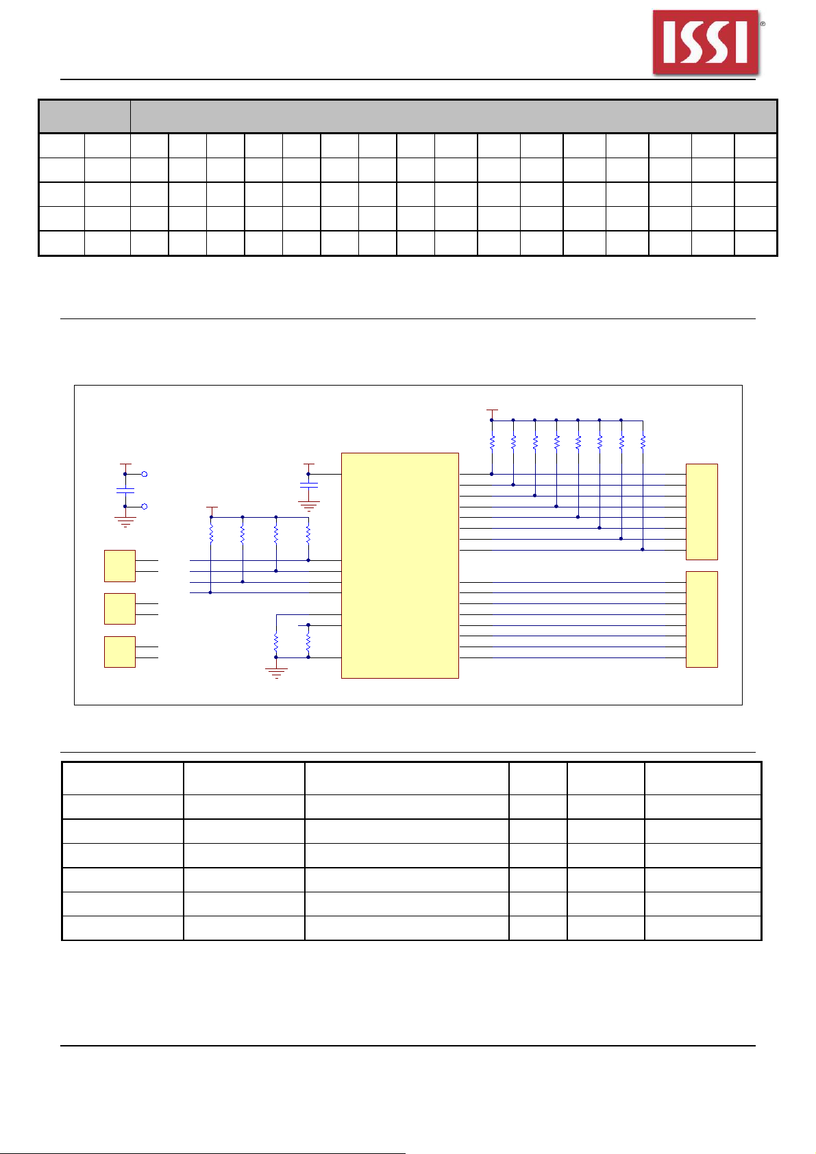
Figure 2:IS31IO7325 Application Schematic
Bill of Materials
Name Symbol Description Qty Supplier Part No.
I/O IC U1 16 I/O Ports.Expander 1 ISSI IS31IO7325
Resistors R1~R4 RES,4.7k,1/16W,±5%,SMD 4
Resistors R5,R6 RES,100k,1/16W,±5%,SMD 2
Resistors R7~R14 RES,100k,1/16W,±5%,SMD 8
Capacitor C1 CAP,10µF,16V,±20%,SMD 1
Capacitor C2 CAP,0.1µF,16V,±20%,SMD 1
Table 3: Bill of Materials, refer to Figure 2 above.
Integrated Silicon Solution, Inc. – www.issi.com
R1.0, 08/13/2012
2
Page 3

IS31IO7325 Multi-Function I/O Driver Evaluation Board Guide
0
1 2
1 2
1212
1 2 3 4 5 6 7 8
2 1
Figure 3: Board Component Placement Guide -Top Layer
0
8
7
6
5
4
3
2
1
00
Figure 4: Board PCB Layout- Top Layer
Integrated Silicon Solution, Inc. – www.issi.com
R1.0, 08/13/2012
3
Page 4

IS31IO7325 Multi-Function I/O Driver Evaluation Board Guide
0
1 2
1 2
1212
1 2 3 4 5 6 7 8
2 1
0
8
7
6
5
4
3
2
1
00
Figure 5: Board Component Placement Guide -Bottom Layer
Figure 6: Board PCB Layout-Bottom Layer
Integrated Silicon Solution, Inc. – www.issi.com
R1.0, 08/13/2012
4
Page 5

IS31IO7325 Multi-Function I/O Driver Evaluation Board Guide
Copyrigh
t © 201
2 Integrated Silicon Solution, Inc. All rights reserved. ISSI reserves the right to make changes to this specification
and its products at any time without notice. ISSI assumes no liability arising out of the application or use of any information,
products or services described herein. Customers are advised to obtain the latest version of this device specification before relying
on any published information and before placing orders for products.
Integrated Silicon Solution, Inc. does not recommend the use of any of its products in life support applications where the failure or
malfunction of the product can reasonably be expected to cause failure of the life support system or to significantly affect its safety
or effectiveness. Products are not authorized for use in such applications unless Integrated Silicon Solution, Inc. receives written
assurance to its satisfaction, that:
a.) the risk of injury or damage has been minimized;
b.) the user assume all such risks; and
c.) potential liability of Integrated Silicon Solution, Inc is adequately protected under the circumstances
Integrated Silicon Solution, Inc. – www.issi.com
5
R1.0, 08/13/2012
 Loading...