

Page 1
36 Channels LED Driver Evaluation Board Guide
Description
IS31FL3236/IS31FL3236A is comprised of 36 constant
current channels each with independent PWM control,
designed for driving LEDs. The output current of each
channel can be set at up to 38mA (Max.) by an
external resistor and independently scaled by a factor
of 1, 1/2, 1/3 and 1/4. The average LED current of
each channel can be changed in 256 steps by
changing the PWM duty cycle through an I2C
interface.
Features
• 2.7V to 5.5V supply
• I2C interface, automatic address increment
function
• Internal reset register
• Modulate LED brightness with 256 steps PWM
• Each channel can be controlled independently
• Each channel can be scaled independently by
• QFN-44 (5mm × 5mm) package
Quick Start
Recommended Equipment
• 5.0V, 2A power supply
Absolute Maximum Ratings
• ≤ 5.5V power supply
Caution: Do not exceed the conditions listed above, otherwise
the board will be damaged.
Procedure
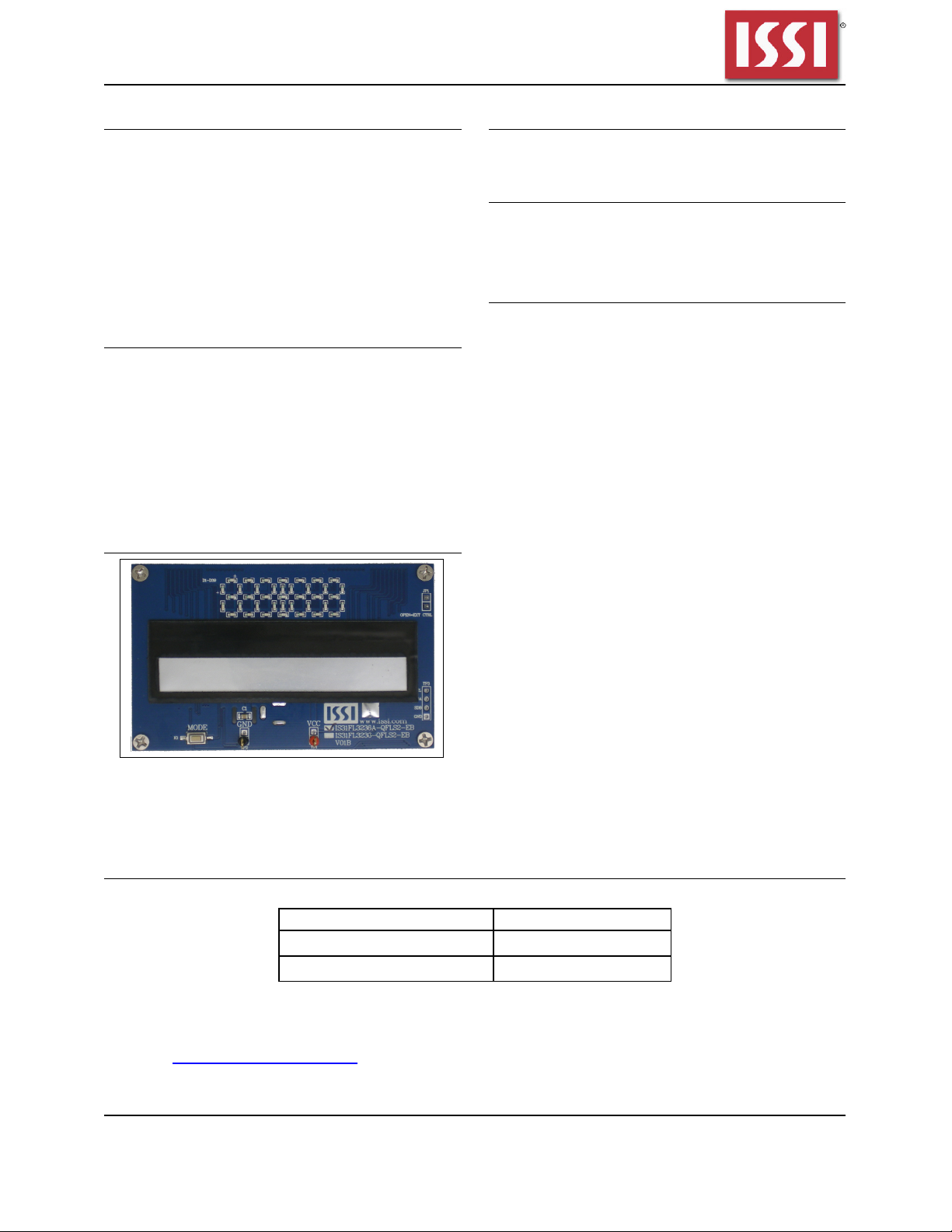
The IS31FL3236/IS31FL3236A evaluation board is
fully assembled and tested. Follow the steps listed
below to verify board operation.
Caution: Do not turn on the power supply until all connections
are completed.
1) Connect the ground terminal of the power supply
to the GND and the positive terminal to the VCC.
Or connect the DC power to the connector (DC
IN).
2) Turn on the power supply and pay attention to the
supply current. If the current exceeds 1.2A,
please check for circuit fault.
3) Enter the desired mode of display by toggling the
MODE button.
Figure 1: Photo of IS31FL3236/IS31FL3236A Evaluation Board
Evaluation Board Ordering Information
Part No. Package
IS31FL3236-QFLS2-EB QFN-44, Lead-free
IS31FL3236A-QFLS2-EB QFN-44, Lead-free
Table1: Ordering Information
For pricing, delivery, and ordering information, please contacts ISSI’s analog marketing
team at analog_mkt@issi.com or (408) 969-6600.
Integrated Silicon Solution, Inc. – www.issi.com 1
Rev. A, 11/18/2016
Page 2
36 Channels LED Driver Evaluation Board Guide
Evaluation Board Operation
The IS31FL3236/IS31FL3236A evaluation board has
six display modes. Press MODE button to switch
configurations.
1) (Default mode) The 12 RGB LEDs in the middle of
the bard show a color changing light bar moving
pattern.
2) Two groups of blue LED on above display a tailing
effect move from right to left.
3) Two groups of blue LED on above display a tailing
effect move in opposite directions.
4) Blue LED on above perform timer display.
5) Two groups of blue LED on above flash together
from two sides to middle and then turn off slowly
from both sides to middle.
6) The blue LEDs on above are put into four ‘8’ digits
and to show a twist effect.
*Note:
IS31FL3236/IS31FL3236A solely controls the FxLED function on
the evaluation board.
VRGB
D40 D41 D42 D43 D44 D45
G G G G G G G G G G G GR R R R R R R R R R R RB B B B B B B B B B B B
OUT 1
OUT 2
OUT 3
OUT 4
OUT 5
OUT 6
OUT 7
OUT 8
OUT 9
OUT 10
OUT 11
OUT 12
OUT 13
OUT 14
OUT 15
OUT 16
OUT 17
Software support
JP1 default setting is close circuit. If it is set to open,
the on-board MCU will stop working. The I2C pins are
set to High Impedance. External I2C signals can be
connected to TP3 to control the IS31FL3236 LED
driver.
Please refer to the datasheet to get more information about
IS31FL3236/IS31FL3236A.
D46 D47 D48 D49 D50 D51
OUT 18
OUT 19
OUT 20
OUT 21
OUT 22
OUT 23
OUT 24
OUT 25
OUT 26
OUT 27
OUT 28
OUT 29
OUT 30
OUT 31
OUT 32
OUT 33
OUT 34
OUT 35
OUT 36
VCC
R5
100KR6100K
CON1
DC IN
U4
1
S1
3
S2
2
G1
G1
G2
G24D2
APM4953
TP1
C3
10uFC11uF
TP2
JP1
OPEN=EXT CTRL G1
VCC
K1
MODE
R7
100K
D1
D1
D2
U3
18
P0.3/CIN1B/KBI3
14
P0.6/CMP1/KBI6
13
P0.7/T1/KBI7
10
P1.2/T0/SCL
11
P1.1/RXD
8
P1.4/INT1
9
P1.3/INT0/SDA
7
P3.0XTAL2/CLKOUT
6
P3.1/XTAL1
3
P1.6
LPC922
VRGB
8
7
VLED
6
5
U2
1
VDD
3
SD
2
GND
LDO
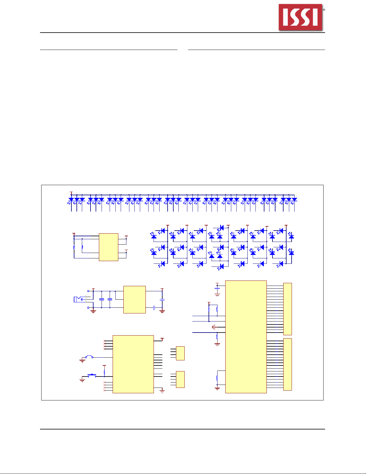
Figure 2:IS31FL3236/IS31FL3236A Application Schematic
VOUT
BP
P0.1/CIN2B/KBI1
P0.2/CIN2A/KBI2
P0.4/CIN1A/KBI4
P0.5/CMPREF/KBI5
P1.0/TXD
P1.5/RST
P0.0/CMP2/KBI0
5
4
VDD
P1.7
VSS
C4
10nF
OUT1
OUT2OUT3
D2
OUT5
D3
OUT4
15
20
19
17
16
12
4
2
1
5
VLED VLED
D1
OUT8
OUT6OUT7
D6
D5
OUT9
D7
D4
OUT10
3VVCC
C5
1uF
3V
GND
SDB
SDA
G2
SCL
P0.4
P0.5
SDB
RST
SDA
3V
SCL
P0.5
P0.4
RST
GND
D20
OUT12OUT13
OUT11
D12
OUT15
D13
OUT14
SDA
SCL
SDB
VLED
D11
D15
D14
VCC
R3
4.7K
D8
D9
D10
TP3
1
2
3
4
TP4
5
4
3
2
1
ICP
OUT16OUT17
C2
1uF
R4
100K
OUT19
D16
OUT19
D17
OUT19
R2
4.7K
R1
3.3K
VCC
VLED
OUT18
D18
D21
OUT18
D19
D22
U1
38
VCC
41
SDA
42
SCL
37
AD
36
SDB
40
R_EXT
17,39
GND
IS31FL3236/IS31FL3236A
OUT21OUT22
OUT20
D24
OUT24
D25
OUT23
VLED
D23
D27
D26
OUT25OUT26
OUT29
OUT27
D28
OUT28
D29
D30
D31
D32
OUT1
OUT2
OUT3
OUT4
OUT5
OUT6
OUT7
OUT8
OUT9
OUT10
OUT11
OUT12
OUT13
OUT14
OUT15
OUT16
OUT17
OUT18
OUT19
OUT20
OUT21
OUT22
OUT23
OUT24
OUT25
OUT26
OUT27
OUT28
OUT29
OUT30
OUT31
OUT32
OUT33
OUT34
OUT35
OUT36
VLED
VLED
D33
OUT30
OUT31OUT32
OUT33
43
44
1
2
3
4
5
6
7
8
9
10
11
12
13
14
15
16
18
19
20
21
22
23
24
25
26
27
28
29
30
31
32
33
34
35
D34
OUT34
D35
OUT1
OUT2
OUT3
OUT4
OUT5
OUT6
OUT7
OUT8
OUT9
OUT10
OUT11
OUT12
OUT13
OUT14
OUT15
OUT16
OUT17
OUT18
OUT19
OUT20
OUT21
OUT22
OUT23
OUT24
OUT25
OUT26
OUT27
OUT28
OUT29
OUT30
OUT31
OUT32
OUT33
OUT34
OUT35
OUT36
OUT35OUT36
D38
D37
D39
D36
TP5
1
2
3
4
5
6
7
8
9
10
11
12
13
14
15
16
17
18
TP6
1
2
3
4
5
6
7
8
9
10
11
12
13
14
15
16
17
18
Integrated Silicon Solution, Inc. – www.issi.com 2
Rev. A, 11/18/2016
Page 3

36 Channels LED Driver Evaluation Board Guide
Bill of Materials
Name Symbol Description Qty Supplier Part No.
LED Driver U1 36 CH FxLED Driver 1 ISSI IS31FL3236/IS31FL3236A
LDO U2 Low-dropout Regulator 1 PAM PAM3101
MCU U3 Microcontroller 1 NXP LPC922
PMOS U4 Dual PMOS 1 ANPEC APM4953
Diode D1~D39 Diode, LED Blue, SMD 39 Everlight 19-217/BHC-ZL1M2RY/3T
Diode D40~D51 Diode, LED RGB, SMD 12 Everlight 99-235/RGBC/TR8
Resistor R1 RES,3.3k,1/16W,±5%,SMD 1 Yageo RC0603JR-073K3L
Resistors R2~R3 RES,4.7k,1/16W,±5%,SMD 2 Yageo RC0603JR-074K7L
Resistors R4~R7 RES,100k,1/16W,±5%,SMD 4 Yageo RC0603JR-07100KL
Capacitor C1 CAP,10µF,16V,±20%,SMD 1 Yageo CC0603KKX7R9BB106
Capacitors C2,C3,C5 CAP, 1µF,16V,±20%,SMD 3 Yageo CC0603KKX7R9BB105
Capacitor C4 CAP,10nF,16V,±20%,SMD 1 Yageo CC0603KKX7R9BB103
Button K1 Button SMD 1
Table 2: Bill of Materials, refer to Figure 2 above.
Integrated Silicon Solution, Inc. – www.issi.com 3
Rev. A, 11/18/2016
Page 4

36 Channels LED Driver Evaluation Board Guide
Figure 3: Board Component Placement Guide -Top Layer
Figure 4: Board PCB Layout- Top Layer
Integrated Silicon Solution, Inc. – www.issi.com 4
Rev. A, 11/18/2016
Page 5

36 Channels LED Driver Evaluation Board Guide
Figure 5: Board Component Placement Guide -Bottom Layer
Figure 6: Board PCB Layout-Bottom Layer
Integrated Silicon Solution, Inc. – www.issi.com 5
Rev. A, 11/18/2016
Page 6

36 Channels LED Driver Evaluation Board Guide
REVISION HISTORY
Revision Detail Information Data
A Initial Release 2016.11.18
Copyright © 2016 Integrated Silicon Solution, Inc. All rights reserved. ISSI reserves the right to make changes to this specification and its
products at any time without notice. ISSI assumes no liability arising out of the application or use of any information, products or services
described herein. Customers are advised to obtain the latest version of this device specification before relying on any published information
and before placing orders for products.
Integrated Silicon Solution, Inc. does not recommend the use of any of its products in life support applications where the failure or
malfunction of the product can reasonably be expected to cause failure of the life support system or to significantly affect its safety or
effectiveness. Products are not authorized for use in such applications unless Integrated Silicon Solution, Inc. receives written assurance to
its satisfaction, that:
a.) the risk of injury or damage has been minimized;
b.) the user assume all such risks; and
c.) potential liability of Integrated Silicon Solution, Inc is adequately protected under the circumstances
Integrated Silicon Solution, Inc. – www.issi.com 6
Rev. A, 11/18/2016
 Loading...