

Page 1
IS31AP4913 Stereo Headphone Driver Evaluation Board Guide
Description
The IS31AP4913 evaluation board is a fully assembled
and tested PCB. The IS31AP4913 is a high quality
stereo headphone driver with 3D-surround and bass
enhancement capability. It also features removal of the
output DC-blocking capacitors for a reduction in
system component count and end cost. 3D-surround
and bass-enhancement are controlled via RC network.
Features
Supply voltage range from 2.7V to 5.5V
Low output noise (8µV)
High SNR (102dB)
-92dB PSRR
No output DC-blocking capacitors
Pulse Count Control serial interface
Available in QFN-20(3mm × 3mm) package
Quick start
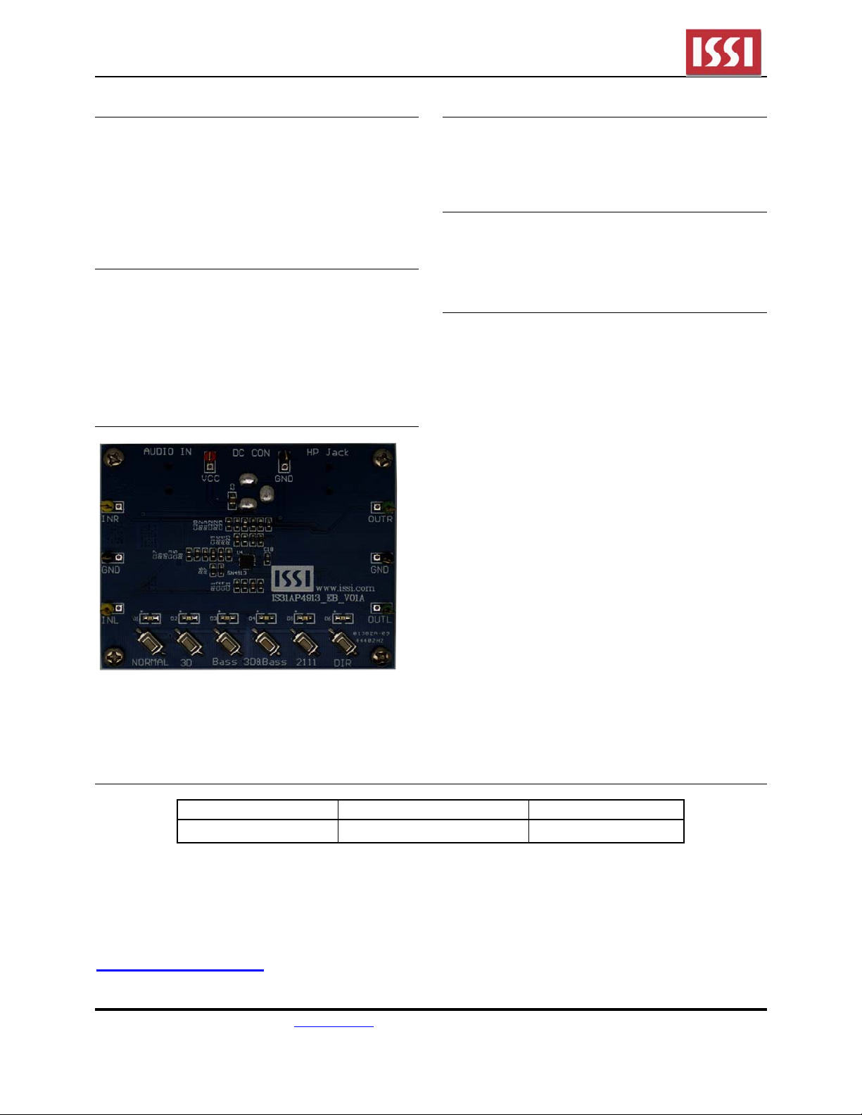
Figure 1 Photo of IS31AP4913 Evaluation Board
Recommended Equipment
5.0V, 2A power supply
Audio source (i.e. MP3 player, Notebook PC, etc.)
Headphone (32Ω)
Absolute Maximum Ratings
≤ 5.5V power supply
Caution: Do not exceed the conditions listed above; otherwise, the
board risks permanent damage.
Procedure
The evaluation board allows verification of
IS31AP4913 device operation.
Caution: Do not turn on the power supply until all connections are
completed.
1. Connect headphone (32Ω) to the connector
(headphone input jack).
2. Connect the ground terminal of the power supply
to the GND and the positive terminal to the VCC.
3. Alternatively, connect DC power to connector (DC
IN).
4. Connect the audio sources to the INR terminal
(right channel) and INL terminal (left channel); or
connect audio source directly to connector
(AUDIO- IN).
5. Turn on the power supply, and pay attention to the
supply current. Be cautious: currents above
200mA are large enough to cause board damage.
6. Turn on the audio source.
Ordering Information
Part No. Temperature Range IC Package
IS31AP4913-QFLS2-EB
For pricing, delivery, and ordering information, please conta ct ISSI at
analog_mkt@issi.com
Integrated Silicon Solution, Inc. – www.issi.com
R1.1, 3/7/2012 1
or (408) 969-6600
-40°C to +85°C (Industrial)
Table 1. Ordering Information
QFN-20, Lead-free
Page 2

IS31AP4913 Stereo Headphone Driver Evaluation Board Guide
Performance Description*
The IS31AP4913 evaluation board has six buttons to switch between the different modes. The operating mode is
indicated by an LED illuminated above the appropriate buttons. The (1~4) modes are performed by IS31AP4913.
1. (Default mode) normal: basic operating mode
2. 3D mode: enable 3D enhance function.
3. Bass mode: enable bass enhance function.
4. 3D&Bass: enable 3D and bass enhance function.
5. 2111: use the output DC-blocking capacitors headphone amplifier (HWD2111) drive headphone
6. DIR: use the input audio source direct drive headphone.
*Note: IS31AP4913 headphone driver provides solely audio function capability on the evaluation board .
Software Support
Please refer to the integrated program.
*Note: Please refer to the datasheet to get more information about IS31AP4913
VDD_5V
J1
2
VDD_5V
R16
10k
key1
SW1
NORMAL
J2
DC CON
C8
0.1uF
J4
INL
J9
OUTL
VDD_5V
C2
10uF
U3
1
VDD
VOUT
3
SD
2
GND
BP
LDO
VDD_5V
1
VCC
2
CON1
3
COM1
4
COFF1
5
NC
INL INR
2
1
OUTL OUTR
2
1
R17
R18
10k
10k
key2
key3
SW3
SW2
Bass
3D
RELAY
1
VCC
J3
2
1
GND
VCC_3V
5
C9
C10
10nF
10uF
4
S1
10
GND
9
CON2
8
COM2
7
COFF2
6
NC
J5
2
1
INR
J10
2
1
OUTR
VCC_3V
R19
R20
10k
10k
key5
key4
SW4
SW5
3D&Bass
2111
key6
INLINR
OUTLOUTR
R21
10k
SW6
DIR
312
P1
ICP
R4
EN_DIR
1k
TRANSISTOR_NPN_3904
Q1
J6
2
1
GND
J11
2
1
GND
VCC_3V
5
EN2111
4
DATA2111
3
RST
2
GND
1
GND
VCC_3V
R14
1k
D1
LED1
D2
LED2
D3
LED3
D4
LED4
D5
LED5
D6
LED6
EN_DIR
LED3
EN4913
CLK2111
DATA2111
EN2111
key 2
key 1
LED1
LED2
key 3
key 4
key 5
RST
LED5
LED4
3
26
25
24
23
22
20
19
18
17
12
11
10
6
5
4
J8
AUDIO IN
U1
P0.0/CMP2/K BI0/AD01
P0.1/CIN2B/KBI1/AD10
P0.2/CIN2A/KBI2/AD11
P0.3/CIN1B/KBI3/AD12
P0.4/CIN 1A/KBI4/DAC1/AD 13
P0.5/CMPREF/KBI5
P0.6/CMP1/KBI6
P0.7/T1/KBI7
P1.0/TXD
P1.1/RXD
P1.2/T0/SCL
P1.3/INT0/SDA
P1.4/INT1
P1.5/RST
P1.6/OCB
P1.7/OCC/AD00
LPC936
INL
INR
C17
0.47uF
C20
0.47uF
Figure 2: IS31AP4913 Application Circuit
P2.0/ICB/DAC0/AD03
P2.1/OCD/AD02
P2.2/MOSI
P2.3/MISO
P2.4/SS
P2.5/SPICLK
P2.6/OCA
P2.7/ICA
P3.0XTAL2/CLKOUT
P3.1/XTAL1
R5
120k
C13
6.8pF
R9
30k
R10
C19 47nF
R11
100k
R12
30k
R22
C23
120k
6.8pF
VDD
VSS
C15
22nFR8510k
4.7k
EN4913
C22
22nF
1
2
13
14
15
16
27
28
9
8
21
7
VCC_3V
R6
20k
R7
20K
R13
510k
R15
20k
R23
20k
C4 0.47uF
INL
INR
C5 0.47uF
DATA2111
CLK2111
key 6
LED6
C11
0.1uF
7
INFL
6
BASSL
5
INL
3
3DR
4
3DL
11
CTRL
2
INR
20
BASER
1
INFR
EN2111
VDD_5V
C12
C14
U4
12
VDD
SGND
PGND
IS31AP4913
10
17
VDD_5V
1uF
C1
10
U2
2
VOUT1
VIN1
VDD
VIN28VOUT2
6
UP/DN
4
CLOCK
7
BYPA SS
SDB
R3
100k
GND
GND
2111
5
1uF
0.1uF
15
OUTL
16
CP
C16
2.2uF
19
CN
18
PVSS
C18
2.2uF
8
NC
9
NC
13
VREF
C21
2.2uF
14
OUTR
C3
C6
J7
HP Jack
OUTL
22uF
OUTR
22uF
1
R1
0R
9
R2
0R
3
C7
0.47uF
OUTL
OUTR
Integrated Silicon Solution, Inc. – www.issi.com
R1.1, 3/7/2012 2
Page 3

IS31AP4913 Stereo Headphone Driver Evaluation Board Guide
Bill of Materials
No. Name Symbol Description Manufacturer PN
1 USB Control U1 Controller LPC936
2 HP Amp U2
3 LDO U3
4 HP Driver U4
5 Relay S1 Panasonic
6 Resistors R1~R23 Refer to Figure 2
6 Capacitors C1~C23 Refer to Figure 2
Table 2: Bill of Materials; Refer to Figure 2 for additional information.
CSMSC Headphone
Driver
Low-Drop Out
Regulator
ISSI Stereo
Headphone Driver
CSMSC HWD2111
EUTECH
IS31AP4913-QFLS2
Integrated Silicon Solution, Inc. – www.issi.com
R1.1, 3/7/2012 3
Page 4

IS31AP4913 Stereo Headphone Driver Evaluation Board Guide
1 2
1 2
1 2
0
0
2
1
2
1
2
1
3
0
1 2
1 2
1 2
0
Figure 3: Board Component Placement Guide -Top Layer
Figure 4: Board PCB Layout- Top Layer
Integrated Silicon Solution, Inc. – www.issi.com
R1.1, 3/7/2012 4
Page 5

IS31AP4913 Stereo Headphone Driver Evaluation Board Guide
1 2
1 2
1 2
0
0
2
1
2
1
2
1
3
0
1 2
1 2
1 2
0
Figure 5: Board Component Placement Guide -Bottom Layer
Figure 6: Board PCB Layout-Bottom Layer
Integrated Silicon Solution, Inc. – www.issi.com
R1.1, 3/7/2012 5
Page 6

IS31AP4913 Stereo Headphone Driver Evaluation Board Guide
Copyright © 2011 Integrated Silicon Solution, Inc. A ll rights reserv ed. ISSI reserves the right to make changes to this specification and
its products at any time without notice. ISSI assumes no liability arising out of the application or use of any information, products or
services described herein. Customers are advised to obtain the latest version of this device specification before relying on any
published information and before placing orders for products.
Integrated Silicon Solution, Inc. does not recommend the use of any of its products in life support applications where the failure or
malfunction of the product can reasonably be expected to cause failure of the life support system or to significantly affect its safety
or effectiveness. Products are not authorized for use in such applications unless Integrated Silicon Solution, Inc. receives written
assurance to its satisfaction, that:
a.) the risk of injury or damage has been minimized;
b.) the user assume all such risks; and
c.) potential liability of Integrated Silicon Solution, Inc is adequately protected under the circumstances.
Integrated Silicon Solution, Inc. – www.issi.com
R1.1, 3/7/2012 6
 Loading...