

Page 1
IS31AP4912 Stereo Headphone Driver Evaluation Board Guide
Description
The IS31AP4912 is stereo headphone drivers
designed to allow the removal of the output
DC-blocking capacitors for reduced component count
and cost. The IS31AP4912 is ideal for small portable
electronics where size and cost are critical design
parameters.
Features
• No output DC-blocking capacitors
• Supply voltage from 2.7V ~ 5.5V
• Low output noise (7µV)
• High SNR (103dB)
• -95dB PSRR
• Thermal protect circuit
• Integrated click-and-pop suppression circuitry
• UTQFN-12 (2mm × 2mm) package
Quick Start
Recommended Equipment
• 5.0V, 2A power supply
• Audio source (i.e. MP3 player, Notebook PC, etc.)
• Headphone (32Ω)
Absolute Maximum Ratings
• ≤ 5.5V power supply
Caution: Do not exceed the conditions listed above; otherwise
the board will be damaged.
Procedure
The IS31AP4912 Evaluation board is fully assembled
and tested. Follow the steps listed below to verify
board operation.
Caution: Do not turn on the power supply until all connections
are completed.
1) Connect headphone (32Ω) to the connector (HP
JACK).
2) Connect the ground terminal of the power supply
to the GND and the positive terminal to the VCC.
Or connect DC power to connector (DC IN).
3) Connect the audio sources to the INR terminal
(right channel) and INL terminal (left channel); or
connect audio sources to the connector (AUDIO
IN).
4) Turn on the power supply, and pay attention to the
supply current. If the current exceeds 200mA,
please check for circuit fault.
5) Turn on the audio sources.
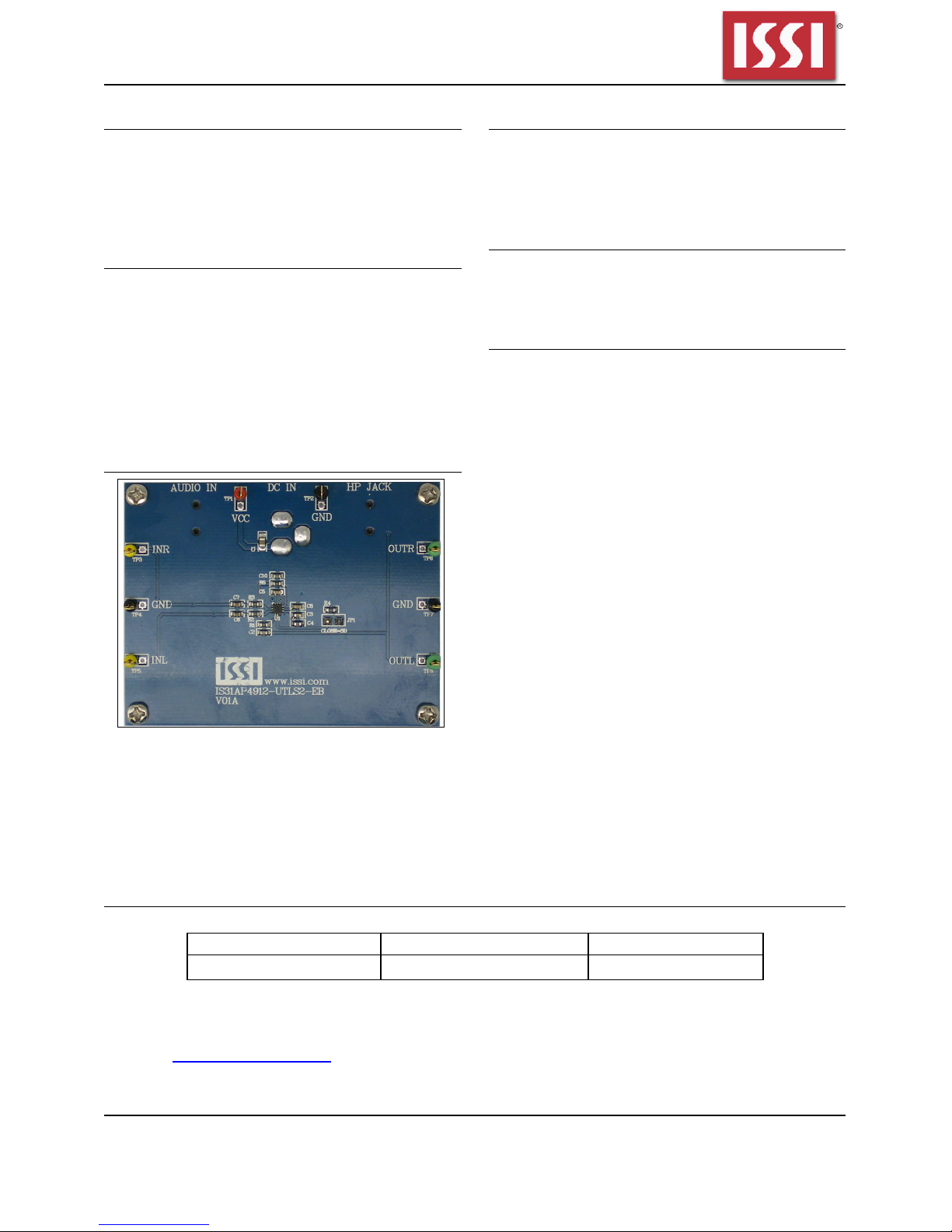
Figure 1: Photo of IS31AP4912 Evaluation Board
Ordering Information
Part No. Temperature Range Package
IS31AP4912-UTLS2-EB -40°C to +85°C (Industrial) UTQFN-12, Lead-free
Table 1: Ordering Information
For pricing, delivery, and ordering information, please contacts ISSI’s analog marketing
team at analog_mkt@issi.com or (408) 969-6600
Integrated Silicon Solution, Inc. – www.issi.com
RevA, 01/10/2013
1
Page 2
IS31AP4912 Stereo Headphone Driver Evaluation Board Guide
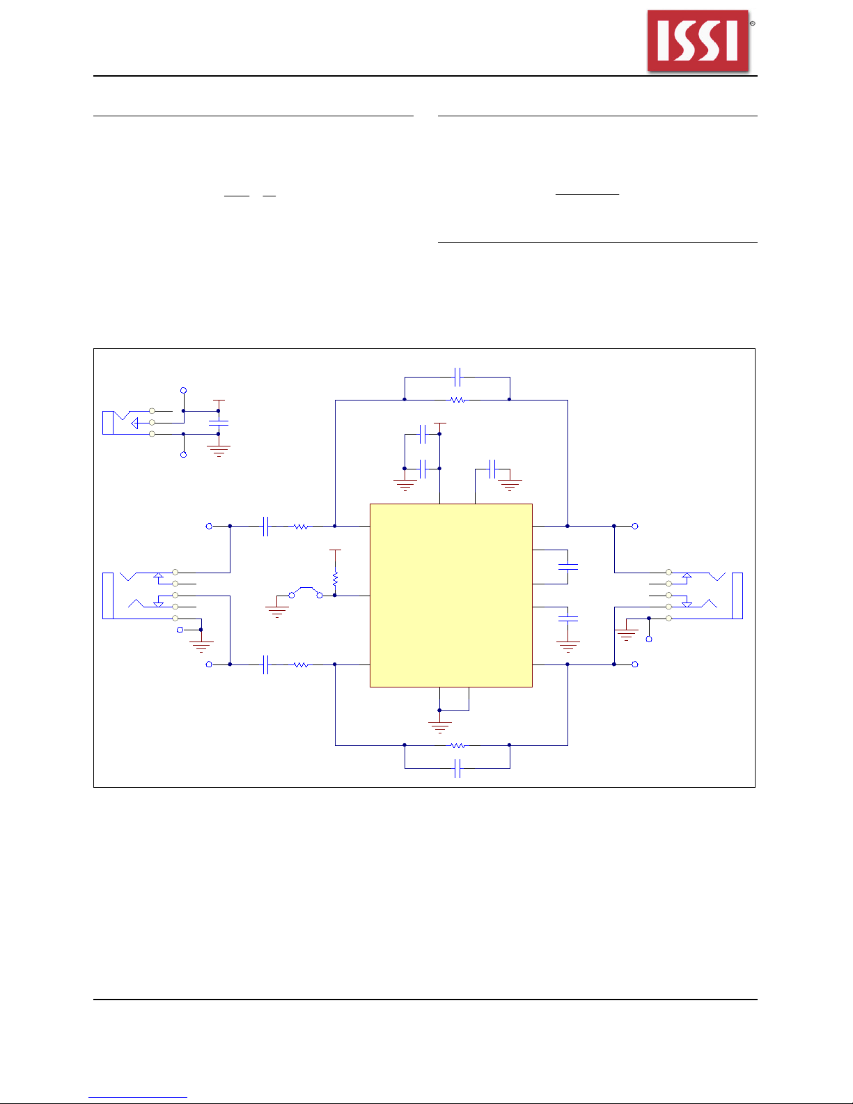
Gain Setting
The input resistors R
RF (R1, R5) set the gain of the amplifier according to
Equation (1).
*Note:
Please refer to the datasheet to get more information about
IS31AP4912.
TP1
CON1
DC IN
TP2
TP5
INL
CON2
AUDIO IN
TP4
TP3
INR
(R2, R3) and feedback resistors
IN
R
V
VCC
R
C1
10uF
F
IN
ain =G
V
C6
0.47uF
C7
0.47uF
(1)
R2
20k
JP1
CLOSE=SD
R3
20k
VCC
R4
100k
U1
3
INL
5
SDB
2
INR
IS31AP4912
High Pass Filter
The input capacitors (C6, C7) and input resistors (R2,
R3) form a high pass filter with the corner frequency, fC,
determined in Equation (2).
1
f
=
c
π
2
CR
ININ
(2)
Shutdown mode
Close Jumper (JP1) enter shutdown mode.
C2
6.8pF
R1
20k
C3
VCC
1uF
C4
0.1uF
7
6
C5
2.2uF
12
CP
CN
4
10
C9
2.2uF
1
8
C8
2.2uF
9
OUTL
PVSS
PVDD
VREF
SGND
OUTR
PGND
11
TP8
OUTL
TP7
TP6
OUTR
CON3
HP JACK
Integrated Silicon Solution, Inc. – www.issi.com
RevA, 01/10/2013
R5
20k
C10
6.8pF
Figure 2: IS31AP4912 Application Schematic
2
Page 3

IS31AP4912 Stereo Headphone Driver Evaluation Board Guide
Bill of Materials
Name Symbol Description Qty Supplier Part No.
Audio Amplifier U1 Stereo Headphone Driver 1 ISSI IS31AP4912
Resistors R1,R2,R3,R5 RES,20k,1/16W,±5%,SMD 4
Resistor R4 RES,100k,1/16W,±5%,SMD 1
Capacitor C1 CAP,10µF,16V,±20%,SMD 1
Capacitors C2,C10 CAP, 6.8pF,16V,±20%,SMD 2
Capacitor C3 CAP,1µF,16V,±20%,SMD 1
Capacitor C4 CAP,0.1µF,16V,±20%,SMD 1
Capacitors C5,C8,C9 CAP,2.2µF,16V,±20%,SMD 3
Capacitors C6,C7 CAP,0.47µF,16V,±20%,SMD 2
Table 2: Bill of Materials, refer to Figure 2 above.
Integrated Silicon Solution, Inc. – www.issi.com
RevA, 01/10/2013
3
Page 4

IS31AP4912 Stereo Headphone Driver Evaluation Board Guide
1 2
1 2
1 2
0
0
2
1
2
1
2
1
3
2 1
0
2 1
2 1
1 2
0
Figure 3: Board Component Placement Guide -Top Layer
Integrated Silicon Solution, Inc. – www.issi.com
RevA, 01/10/2013
Figure 4: Board PCB Layout- Top Layer
4
Page 5

IS31AP4912 Stereo Headphone Driver Evaluation Board Guide
1 2
1 2
1 2
0
0
2
1
2
1
2
1
3
2 1
0
2 1
2 1
1 2
0
Figure 5: Board Component Placement Guide -Bottom Layer
Integrated Silicon Solution, Inc. – www.issi.com
RevA, 01/10/2013
Figure 6: Board PCB Layout-Bottom Layer
5
Page 6

IS31AP4912 Stereo Headphone Driver Evaluation Board Guide
Copyright © 201
3 Integrated Silicon Solution, Inc. All rights reserved. ISSI reserves the right to make changes to th
is specification and
its products at any time without notice. ISSI assumes no liability arising out of the application or use of any information, products or
services described herein. Customers are advised to obtain the latest version of this device specification before relying on any
published information and before placing orders for products.
Integrated Silicon Solution, Inc. does not recommend the use of any of its products in life support applications where the failure or
malfunction of the product can reasonably be expected to cause failure of the life support system or to significantly affect its safety or
effectiveness. Products are not authorized for use in such applications unless Integrated Silicon Solution, Inc. receives written
assurance to its satisfaction, that:
a.) the risk of injury or damage has been minimized;
b.) the user assume all such risks; and
c.) potential liability of Integrated Silicon Solution, Inc is adequately protected under the circumstances
Integrated Silicon Solution, Inc. – www.issi.com
6
RevA, 01/10/2013
 Loading...