

Page 1
IS31AP2031 CLASS-K AUDIO POWER AMPLIFIER
EVALUATION BOARD GUIDE
Integrated Silicon Solution, Inc. – www.issi.com 1
Rev. C, 01/22/2017
DESCRIPTION
The IS31AP2031 is a Class-K audio power amplifier
with automatic gain control. It drives up to 2.0W (10%
THD+N) into an 8Ω speaker from a 4.2V VCC supply.
The IS31AP2031 provides low cost, space saving
solution for portable equipments which need audio
output with higher power by boosting up supply voltage.
Its external components just include a few capacitors
and resistors (no inductor). The IS31AP2031 use fully
differential design to reduce RF noise. The
IS31AP2031 integrates de-pop circuitry to reduce pop
and click noise during power on/off or shutdown enable
operation. The IS31AP2031 also integrates thermal
and short circuit protection function.
FEATURES
Operates from 2.7V to 4.5V
2.0W into an 8Ω load from a 4.2V supply (10%
THD+N)
4 gain levels: 12dB, 16dB, 24dB, 27.5dB
AGC function
Pulse Count Control serial interface
8kV HBM ESD
Thermal and short-circuit protection
Available in QFN-20 (3mm × 3mm).
QUICK START
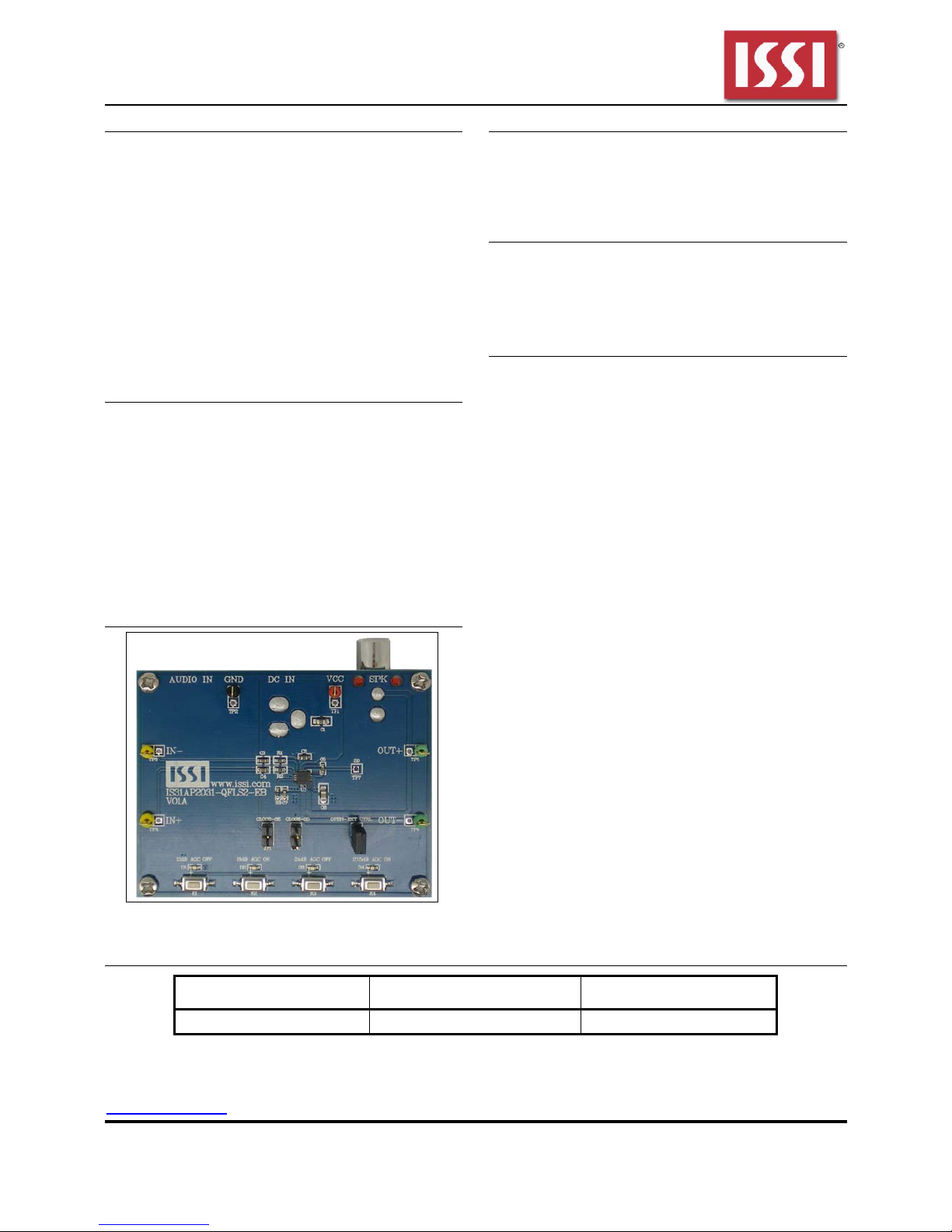
Figure 1: Photo of IS31AP2031 Evaluation Board
RECOMMENDED EQUIPMENT
≤ 4.5V, 2A power supply
Audio source (i.e. MP3 player, Notebook PC, etc.)
An 8Ω speaker
ABSOLUTE MAXIMUM RATINGS
≤ 4.5V power supply
Caution: Do not exceed the conditions listed above; otherwi se
the board will be damaged
PROCEDURE
The IS31AP2031 demo board is fully assembled and
tested. Follow the steps listed below to verify board
operation.
Caution: Do not turn on the power supply until all connections
are completed.
1) Connect an 8Ω (or larger) speaker across the
OUT- terminal and OUT+ terminal.
2) Connect the ground terminal of the power supply
to the GND and the positive terminal to the VCC.
Or connect DC power to connector (DC IN).
3) If the audio source is differential, remove jumper
JP1, connect the negative of the audio source to
the IN- terminal, and connect the positive of the
audio source to IN+ terminal.
4) If the audio source is single-ended, connect the
audio source to the IN- terminal, and close jumper
JP1; or connect audio source to the audio
connector (AUDIO IN) and close jumper JP1.
5) Turn on the power supply, and pay attention to the
supply current. If the current exceeds 1.5A,
please check for circuit fault.
6) Turn on the audio source.
ORDERING INFORMATION
Part No. Temperature Range Package
IS31AP2031-QFLS2-EB -40°C to +85°C (Industrial) QFN-20, Lead-free
Table 1: Ordering Information
For pricing, delivery, and ordering information, please contacts ISSI’s analog marketing team at
analog@issi.com
or (408) 969-660.
Page 2
IS31AP2031 CLASS-K AUDIO POWER AMPLIFIER
EVALUATION BOARD GUIDE
Integrated Silicon Solution, Inc. – www.issi.com 2
Rev. C, 01/22/2017
PERFORMANCE DESCRIPTION
The IS31AP2031 evaluation board has four buttons to
switch between the different modes. The operating
mode is indicated by an LED illuminated above the
appropriate buttons. The modes listed as below:
1) Mode1: gain level 12dB AGC OFF.
2) Mode2: gain level 16dB AGC ON.
3) Mode3: gain level 24dB AGC OFF.
4) Mode4: gain level 27.5dB: AGC ON.
5) Shutdown mode: close Jumper (JP2) enter
shutdown mode.
Note: IS31AP2031 Audio Amplifier provides solely the Audio
function on the evaluation board.
SOFTWARE SUPPORT
Please refer to the integrated program.
Note: The Jumper JP3 is closed by default, if the JP3 is open,
the MCU will stop functioning, the SDB pin of the chip in a h igh
impedance state. The external MCU can be used to control the
board SD (TP7) point.
Please refer to the datasheet to get more information about
IS31AP2031.
P0.0
1
P1.7
2
P1.6
3
RST
4
GND
5
OSC 1
6
OSC 2
7
INT1/P1.4
8
INT0/P1.3
9
T0/P1.2
10
RXD/P1.1
11
TXD/P1.0
12
T1/P0.7
13
P0.1
20
P0.2
19
P0.3
18
P0.4
17
P0.5
16
VDD
15
P0.6
14
U3
LPC922
K427.5dB AGC ON
K324dB AGC OFF
K216dB AGC ON
K112dB AGC OFF
D2
D3
D4
D1
R8
1K
R9
1K
R7
1K
3V
1uF
C2
4.7uF
C5
10uF
C6
C3
15nF
C4
15nF
0.1uF
C7
R1
10K
R2
10K
Speaker
100K
R3
VCC
CLOSE= SE
JP1
R10
100K
R13
100K
R12
100K
R11
100K
R6
1K
VDD
4,8
SDB
1
IN-
6
IN+
7
FS
9
AVIN
12,17,18
CP
3
CN
19
OUT+
15
OUT-
13
GND
14,20
U1
IS31AP2031
VDD
1
GND
2
SD
3
BP
4
VOUT
5
U2
LDO
C8
1uF
C10
1uF
C9
10nF
VCC 3V
VCC
SDB
SDB
LED1
LED2
LED3
LED4LED1
LED2
LED3
LED4
R4
NC
R5
100K
SD
TP7
CLOSE= SD
JP2
VCC
3V
OPEN=EXT CTRL
JP3
TP3
TP4
IN-
IN+
OUT+
TP5
OUT-
TP6
CON3
SPK
VCC
C1
10uF
CON1
DC IN
TP1
TP2
CON2
AUDIO IN
1
2
3
4
5
TP8
ICP
3V
P0.5
P0.4
RST
GND
RST
P0.5
P0.4
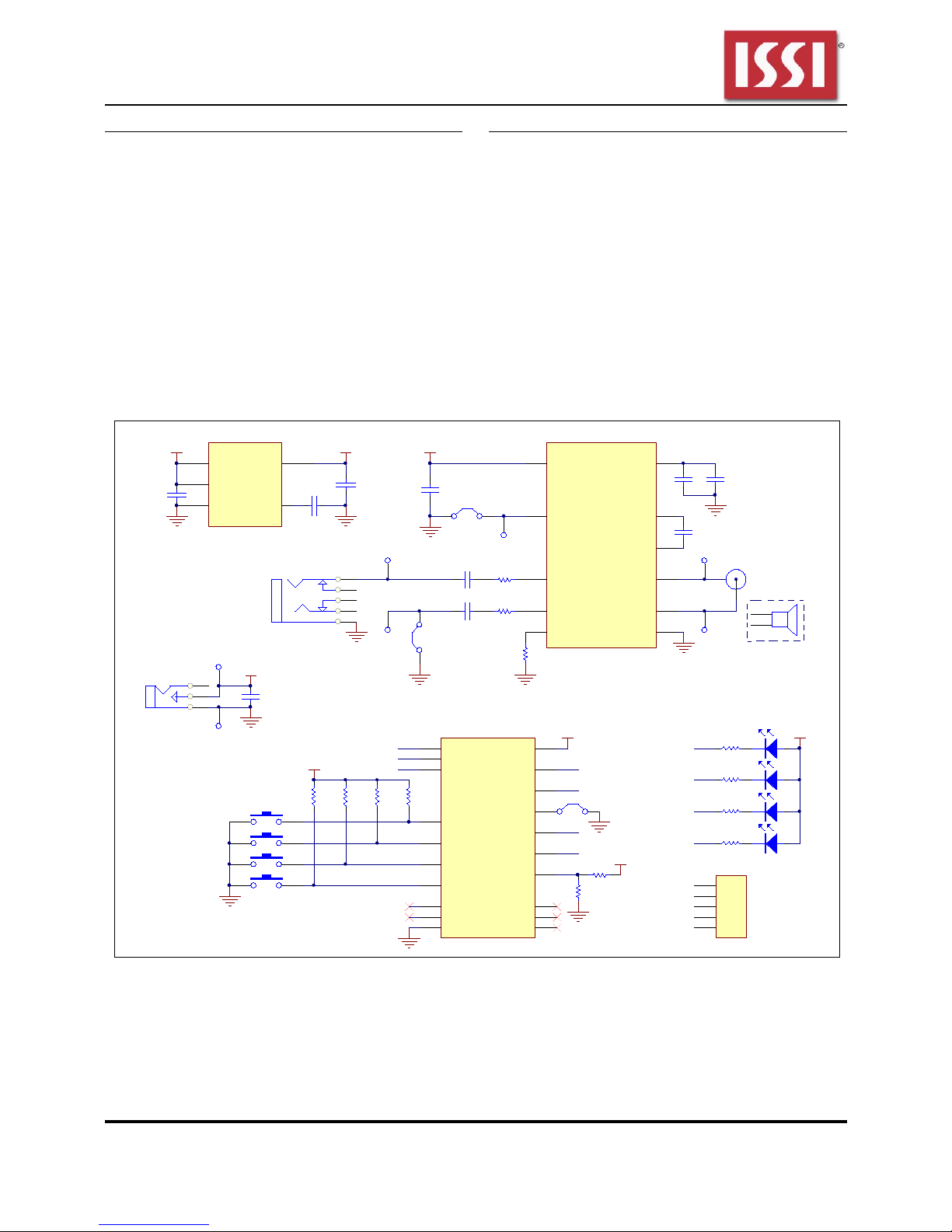
Figure 2: IS31AP2031 Application Schematic
Page 3

IS31AP2031 CLASS-K AUDIO POWER AMPLIFIER
EVALUATION BOARD GUIDE
Integrated Silicon Solution, Inc. – www.issi.com 3
Rev. C, 01/22/2017
BILL OF MATERIALS
Name Symbol Description Qty Supplier Part No.
Audio Amplifier U1 Class-K Audio Amplifier 1 ISSI IS31AP2031
LDO U2 Low-dropout Regulator 1 PAM PAM3101
MCU U3 Microcontroller 1 NXP LPC922
Diode D1~D4 Diode, LED Blue, SMD 4 Everlight 19-217/BHC-ZL1M2RY/3T
Resistor R1,R2 RES,10k,1/16W,±1%,SMD 2 Yageo RC0603FR-0710KRL
Resistor R3,R5,R10~R13 RES,100k,1/16W,±5%,SMD 6 Yageo RC0603JR-07100KRL
Resistor R6~R9 RES,1k,1/16W,±5%,SMD 4 Yageo RC0603JR-0701KRL
Resistor R4 Not Connected 1
Capacitor C1,C6 CAP,10µF,10V,±10%,SMD 2 Yageo CC0805KKX7R6BB106
Capacitor C2 CAP, 1µF,16V,±10%,SMD 1 Yageo CC0603KKX7R7BB105
Capacitor C8,C10 CAP, 1µF,16V,±10%,SMD 2 Yageo CC0805KKX7R7BB105
Capacitor C3,C4 CAP, 15nF,16V,±10%,SMD 2 Yageo CC0603KKX7R7BB153
Capacitor C5 CAP, 4.7µF,10V,±10%,SMD 1 Yageo CC0805KKX7R6BB475
Capacitor C7 CAP, 0.1µF,16V,±10%,SMD 1 Yageo CC0603KKX7R7BB104
Capacitor C9 CAP,10nF,16V,±10%,SMD 1 Yageo CC0603KKX7R7BB103
Button K1~K4 Button SMD 4
Bill of Materials, refer to Figure 2 above.
Page 4

IS31AP2031 CLASS-K AUDIO POWER AMPLIFIER
EVALUATION BOARD GUIDE
Integrated Silicon Solution, Inc. – www.issi.com 4
Rev. C, 01/22/2017
0
0 0
0
2
1
2
2
2
2
1
1 2 1 2
1 2
1
2
1
2
1 2
1
2 2
1
2
Figure 3: Board Component Placement Guide - Top Layer
Figure 4: Board PCB Layout - Top Layer
Page 5

IS31AP2031 CLASS-K AUDIO POWER AMPLIFIER
EVALUATION BOARD GUIDE
Integrated Silicon Solution, Inc. – www.issi.com 5
Rev. C, 01/22/2017
0
0 0
0
2
1
2
2
2
2
1
1 2 1 2
1 2
1
2
1
2
1 2
1
2 2
1
2
Figure 5: Board Component Placement Guide - Bottom Layer
Figure 6: Board PCB Layout - Bottom Layer
Copyright © 2017 Integrated Silicon Solution, Inc. All rights reserved. ISSI reserves the right to make changes to this specification and its
products at any time without notice. ISSI assumes no liability arising out of the application or use of any information, products or services
described herein. Customers are advised to obtain the latest version of this device specification before relying on any published information
and before placing orders for products.
Integrated Silicon Solution, Inc. does not recommend the use of any of its products in life support applications where the failure or
malfunction of the product can reasonably be expected to cause failure of the life support system or to significantly affect its safety or
effectiveness. Products are not authorized for use in such applications unless Integrated Silicon Solution, Inc. receives written assurance to
its satisfaction, that:
a.) the risk of injury or damage has been minimized;
b.) the user assume all such risks; and
c.) potential liability of Integrated Silicon Solution, Inc is adequately protected under the circumstances
 Loading...