


IS24C01-2 IS24C01-3 IS24C02-2 IS24C02-3
®
IS24C08-2 IS24C08-3 IS24C16-2 IS24C16-3
ISSI
1K-bit/2K-bit/8K-bit/16K-bit 2-WIRE
SERIAL CMOS EEPROM
FEATURES
• Low Power CMOS Technology
-- Standby Current less than 8 µA (5.5V)
-- Read Current (typical) less than 1 mA (5.5V)
-- Write Current (typical) less than 3 mA (5.5V)
• Low Voltage Operation
-- IS24C01-2, IS24C02-2, IS24C08-2 &
IS24C16-2: Vcc = 1.8V to 5.5V
-- IS24C01-3, IS24C02-3, IS24C08-3 &
IS24C16-3: Vcc = 2.5V to 5.5V
• 100 KHz (1.8V) and 400 KHz (5V) Compatibility
• Hardware Data Protection
-- Write Protect Pin
• Sequential Read Feature
• Filtered Inputs for Noise Suppression
• 8-pin PDIP and 8-pin SOIC packages
• Self time write cycle with auto clear
-- 5 ms @ 2.5V
• Organization:
-- IS24C01-2 and IS24C01-3: 128x8
(one block of 128 bytes)
-- IS24C02-2 and IS24C02-3: 256x8
(one block of 256 bytes)
-- IS24C08-2 and IS24C08-3: 1024x8
(four blocks of 256 bytes)
-- IS24C16-2 and IS24C16-3: 2048x8
(eight blocks of 256 bytes)
• Page Write Buffer
• Two-Wire Serial Interface
-- Bi-directional data transfer protocol
• High Reliability
-- Endurance: 1,000,000 Cycles
-- Data Retention: 100 Years
• Commercial and Industrial temperature ranges
OCTOBER 2000
PRODUCT OFFERING OVERVIEW
Part No Voltage Speed Standby ICC Read ICC Write ICC Temperature
IS24C01-2 1.8V-5.5V 100 KHz < 4 µA 1 mA 3 mA C,I
IS24C01-3 2.5V-5.5V 400 KHz < 8 µA 1 mA 3 mA C,I
IS24C02-2 1.8V-5.5V 100 KHz < 4 µA 1 mA 3 mA C,I
IS24C02-3 2.5V-5.5V 400 KHz < 8 µA 1 mA 3 mA C,I
IS24C08-2 1.8V-5.5V 100 KHz < 4 µA 1 mA 3 mA C,I
IS24C08-3 2.5V-5.5V 400 KHz < 8 µA 1 mA 3 mA C,I
IS24C16-2 1.8V-5.5V 100 KHz < 4 µA 1 mA 3 mA C,I
IS24C16-3 2.5V-5.5V 400 KHz < 8 µA 1 mA 3 mA C,I
DESCRIPTION
The IS24C01-2 is a 1.8V 1K-bit EEPROM, IS24C01-3 is
a 2.5V 1K-bit EEPROM, IS24C02-2 is a 1.8V 2K-bit
EEPROM, IS24C02-3 is a 2.5V 2K-bit EEPROM, IS24C082 is a 1.8V 8K-bit EEPROM, IS24C08-3 is a 2.5V 8K-bit
EEPROM, IS24C16-2 is a 1.8V 16K-bit EEPROM, and the
IS24C16-3 is a 2.5V 16K-bit EEPROM.
The IS24CXX (IS24C01-2, IS24C01-3, IS24C02-2,
IS24C02-3, IS24C08-2, IS24C08-3, IS24C16-2 and
IS24C16-3) family is a low-cost and low voltage 2-wire
Serial EEPROM. It is fabricated using ISSI’s advanced
CMOS EEPROM technology and provides a low power
and low voltage operation. The IS24CXX family features
a write protection feature, and is available in 8-pin DIP and
8-pin SOIC packages.
ISSI reserves the right to make changes to its products at any time without notice in order to improve design and supply the best possible product. We assume no responsibility for any
errors which may appear in this publication. © Copyright 2001, Integrated Silicon Solution, Inc.
Integrated Silicon Solution, Inc. — 1-800-379-4774
Rev. B
02/27/01
1
IS24C01-2 IS24C01-3 IS24C02-2 IS24C02-3
IS24C08-2 IS24C08-3 IS24C16-2 IS24C16-3 ISSI
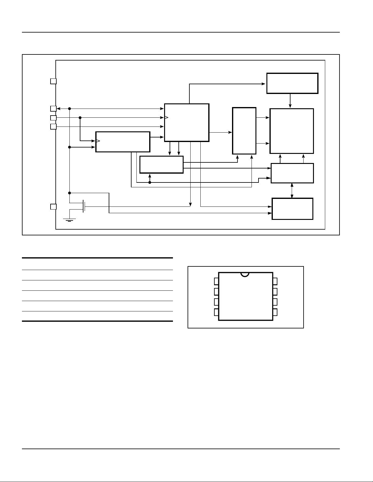
FUNCTIONAL BLOCK DIAGRAM
®
8
Vcc
5
SDA
6
SCL
7
WP
4
GND
nMOS
PIN DESCRIPTIONS
A0-A2 Address Inputs
SLAVE ADDRESS
REGISTER &
COMPARATOR
CONTROL
LOGIC
WORD ADDRESS
COUNTER
ACK
X
DECODER
Clock
DI/O
PIN CONFIGURATION
8-Pin DIP and SOIC
HIGH VOLTAGE
GENERATOR,
TIMING & CONTROL
EEPROM
ARRAY
Y
DECODER
DATA
>
REGISTER
SDA Serial Address/Data I/O
SCL Serial Clock Input
WP Write Protect Input
Vcc Power Supply
GND Ground
SCL
This input clock pin is used to synchronize the data
transfer to and from the device.
SDA
The SDA is a Bi-directional pin used to transfer addresses and data
into and out of the device. The SDA pin is an open drain output and
can be wire-Ored with other open drain or open collector outputs.
The SDA bus
requires
a pullup resistor to Vcc.
A0, A1, A2
The A0, A1 and A2 are the device address inputs. The IS24C01 and
IS24C02 use the A0, A1, and A2 for hardware addressing and a
total of 8 devices may be used on a single bus system
The IS24C08-2 and IS24C08-3 only use A2 input for hardwire
8
A0
A1
A2
GND
1
2
3
4
VCC
7
WP
6
SCL
5
SDA
addressing and a total of two devices may be addressed on a single
bus system. The A0 and A1 pins are not used by IS24C08-2 and
IS24C08-3. They may be left floating or tied to either GND or Vcc.
These pins are not used by IS24C16-2 and IS24C16-3. A0 and A1
may be left floating or tied to either GND or Vcc. A2 should be tied
to either GND or Vcc.
WP
WP is the Write Protect pin. On the 24C01, 24C02 and
24C08, if the WP pin is tied to VCC the entire array becomes
Write Protected (Read only). On the 24C16, if the WP pin
is tied to Vcc the upper half array becomes Write Protected
(Read only). When WP is tied to GND or left floating normal
read/write operations are allowed to the device.
2
Integrated Silicon Solution, Inc. — 1-800-379-4774
Rev. B
02/27/01

IS24C01-2 IS24C01-3 IS24C02-2 IS24C02-3
IS24C08-2 IS24C08-3 IS24C16-2 IS24C16-3 ISSI
®
DEVICE OPERATION
The IS24CXX family features a serial communication and
supports a bi-directional 2-wire bus transmission protocol.
2-WIRE BUS
The two-wire bus is defined as a Serial Data line(SDA),
and a Serial Clock Line (SCL). The protocol defines any
device that sends data onto the SDA bus as a transmitter,
and the receiving devices as a receiver. The bus is
controlled by MASTER device which generates the SCL,
controls the bus access and generates the STOP and
START conditions. The IS24CXX is the SLAVE device on
the bus.
The Bus Protocol:
-- Data transfer may be initiated only when the bus is not
busy
-- During a data transfer, the data line must remain stable
whenever the clock line is high. Any changes in the data
line while the clock line is high will be interpreted as a
START or STOP condition.
The state of the data line represents valid data when after
a START condition, the data line is stable for the duration
of the HIGH period of the clock signal. The data on the line
must be changed during the LOW period of the clock
signal. There is one clock pulse per bit of data. Each data
transfer is initiated with a START condition and terminated
with a STOP condition.
START Condition
The START condition precedes all commands to the
devices and is defined as a HIGH to LOW transition of SDA
when SCL is HIGH. The IS24CXX monitors the SDA and
SCL lines and will not respond until the START condition
is met.
STOP Condition
The STOP condition is defined as a LOW to HIGH transition
of SDA when SCL is HIGH. All operations must end with
a STOP condition.
ACKnowledge
After a successful data transfer, each receiving device is
required to generate an acknowledge. The Acknowledging
device pulls down the SDA line.
DEVICE ADDRESSING
The MASTER begins a transmission by sending a START
condition. The MASTER then sends the address of the
particular slave devices it is requesting. The SLAVE (Fig.
5) address is 8 bits.
The four most significant bits of the address are fixed as
1010 for the IS24CXX.
For the IS24C16-2 and IS24C16-3, the bits(B2, B1 and B0)
are used for memory page addressing (the IS24C16-2 and
IS24C16-3 are organized as eight blocks of 256 bits).
For the IS24C08-2 and IS24C08-3 out of the next three
bits, B1 and B0 are for memory page addressing (the
IS24C08-2 and IS24C08-3 are organized as four blocks of
256 bits) and the A2 bit is used as device address bit and
must compare to its hard-wired input pin (A2). Up to two
IS24C08 may be individually addressed by the system.
The page addressing bits for IS24CXX should be
considered the most significant bits of the data word
address which follows.
For the IS24C01/2-2 and IS24C01/2-3, the A0, A1, and A2
are used as device address bits and must compare to its
hard-wired input pins (A0, A1, and A2) Up to Eight
IS24C01/2's may be individually addressed by the system.
The last bit of the slave address specifies whether a Read
or Write operation is to be performed. When this bit is set
to 1, a Read operation is selected, and when set to 0, a
Write operation is selected.
After the MASTER sends a START condition and the
SLAVE address byte, the IS24CXX monitors the bus and
responds with an Acknowledge (on the SDA line) when its
address matches the transmitted slave address. The
IS24CXX pulls down the SDA line during the ninth clock
cycle, signaling that it received the eight bits of data. The
IS24CXX then performs a Read or Write operation
depending on the state of the R/W bit.
WRITE OPERATION
Byte Write
In the Byte Write mode, the Master device sends the
START condition and the slave address information(with
the R/W set to Zero) to the Slave device. After the Slave
generates an acknowledge, the Master sends the byte
address that is to be written into the address pointer of the
IS24CXX. After receiving another acknowledge from the
Slave, the Master device transmits the data byte to be
written into the address memory location. The IS24CXX
acknowledges once more and the Master generates the
STOP condition, at which time the device begins its
internal programming cycle. While this internal cycle is in
progress, the device will not respond to any request from
the Master device.
Page Write
The IS24CXX is capable of page-WRITE (8-byte for
24C01/2 and 16-byte for 24C08/16) operation. A pageWRITE is initiated in the same manner as a byte write, but
instead of terminating the internal write cycle after the first
data word is transferred, the master device can transmit
up to N more bytes (N=7 for 24C01/2 and N=15 for 24C08/
16). After the receipt of each data word, the IS24CXX
Integrated Silicon Solution, Inc. — 1-800-379-4774
Rev. B
02/27/01
3

IS24C01-2 IS24C01-3 IS24C02-2 IS24C02-3
IS24C08-2 IS24C08-3 IS24C16-2 IS24C16-3 ISSI
®
responds immediately with an ACKnowledge on SDA line,
and the three lower (24C01/24C02) or four lower (24C08/
24C16) order data word address bits are internally
incremented by one, while the higher order bits of the data
word address remain constant. If the master device
should transmit more than N+1 (N=7 for 24C01/2 and
N=15 for 24C08/16) words, prior to issuing the STOP
condition, the address counter will “roll over,” and the
previously written data will be overwritten. Once all N+1
(N=7 for 24C01/2 and N=15 for 24C08/16) bytes are
received and the STOP condition has been sent by the
Master, the internal programming cycle begins. At this
point, all received data is written to the IS24CXX in a
single write cycle. All inputs are disabled until completion
of the internal WRITE cycle.
Acknowledge Polling
The disabling of the inputs can be used to take advantage
of the typical write cycle time. Once the stop condition is
issued to indicate the end of the host's write operation, the
IS24CXX initiates the internal write cycle. ACK polling can
be initiated immediately. This involves issuing the start
condition followed by the slave address for a write operation.
If the IS24CXX is still busy with the write operation, no ACK
will be returned. If the IS24CXX has completed the write
operation, an ACK will be returned and the host can then
proceed with the next read or write operation.
READ OPERATION
READ operations are initiated in the same manner as
WRITE operations, except that the read/write bit of the
slave address is set to “1”. There are three READ operation
options: current address read, random address read and
sequential read.
Current Address Read
The IS24CXX contains an internal address counter which
maintains the address of the last byte accessed,
incremented by one. For example, if the previous operation
is either a read or write operation addressed to the address
location n, the internal address counter would increment to
address location n+1. When the IS24CXX receives the
Device Addressing Byte with a READ operation (read/
write bit set to “1”), it will respond an ACKnowledge and
transmit the 8-bit data word stored at address location
n+1. The master will not acknowledge the transfer but
does generate a STOP condition and the IS24CXX
discontinues transmission. If 'n' is the last byte of the
memory, then the data from location '0' will be transmitted.
(Refer to Current Address Read Diagram.)
Random Access Read
Selective READ operations allow the Master device to
select at random any memory location for a READ operation.
The Master device first performs a 'dummy' write operation
by sending the START condition, slave address and word
address of the location it wishes to read. After the IS24CXX
acknowledge the word address, the Master device resends
the START condition and the slave address, this time with
the R/W bit set to one. The IS24CXX then responds with
its acknowledge and sends the data requested. The master
device does not send an acknowledge but will generate a
STOP condition. (Refer to Random Address Read
Diagram.)
Sequential Read
Sequential Reads can be initiated as either a Current
Address Read or Random Address Read. After the
IS24CXX sends initial byte sequence, the master device
now responds with an ACKnowledge indicating it requires
additional data from the IS24CXX. The IS24CXX continues
to output data for each ACKnowledge received. The master
device terminates the sequential READ operation by pulling
SDA HIGH (no ACKnowledge) indicating the last data
word to be read, followed by a STOP condition.
The data output is sequential, with the data from
address n followed by the data from address n+1, ... etc.
The address counter increments by one automatically,
allowing the entire memory contents to be serially read
during sequential read operation. When the memory
address boundary (127 for IS24C01-2 and IS24C01-3; 255
for IS24C02-2 and IS24C02-3; 1023 for IS24C08-2 and
IS24C08-3; 2047 for IS24C16-2 and IS24C16-3) is reached,
the address counter “rolls over” to address 0, and the
IS24CXX-2 continues to output data for each ACKnowledge
received. (Refer to Sequential Read Operation Starting
with a Random Address READ Diagram.)
4
Integrated Silicon Solution, Inc. — 1-800-379-4774
Rev. B
02/27/01

IS24C01-2 IS24C01-3 IS24C02-2 IS24C02-3
IS24C08-2 IS24C08-3 IS24C16-2 IS24C16-3 ISSI
®
SDA
SCL
Typical System Bus Configuration
SCL from
Master
Data Output
from
Transmitter
Data Output
from
Receiver
Vcc
Master
Transmitter/
Receiver
IS24Cxx
189
t
AA
t
AA
ACK
Output Acknowledge
SCL
START
Condition
SDA
START and STOP Conditions
Condition
STOP
Integrated Silicon Solution, Inc. — 1-800-379-4774
Rev. B
02/27/01
5

IS24C01-2 IS24C01-3 IS24C02-2 IS24C02-3
IS24C08-2 IS24C08-3 IS24C16-2 IS24C16-3 ISSI
Data Validity Protocol
Data Change
SCL
Data Stable Data Stable
SDA
Slave Address
7BIT 43 12560
0101
7BIT 43 12560
0101
A0A1A2
R/W
B0B1A2
R/W
IS24C01
IS24C02
IS24C08
®
Byte Write
Page Write
SDA
Bus
Activity
S
T
A
R
T
M
S
B
Device
Address
MSB
S
T
A
R
T
SDA
Bus
Activity
W
R
I
T
Word Address (n)
E
A
C
K
L
S
B
R/W
7BIT 43 12560
Data (n+1) Data (n)
Data
IS24C16
S
T
O
P
A
C
K
Data (n+P*)
A
C
K
M
S
B
Device
Address
L
S
B
R/W
0101
W
R
I
T
E
A
C
K
A
C
K
Word Address
M
S
B
B0B1B2
R/W
LSB
A
C
K
A
C
K
* P = 7 for IS24C01 and IS24C02
P = 15 for IS24C08 and IS24C16
S
T
O
P
A
C
K
6
Integrated Silicon Solution, Inc. — 1-800-379-4774
Rev. B
02/27/01

IS24C01-2 IS24C01-3 IS24C02-2 IS24C02-3
IS24C08-2 IS24C08-3 IS24C16-2 IS24C16-3 ISSI
Current Access Read
S
Random Access Read
SDA
Bus
Activity
T
A
R
T
Device
Address
M
S
B
L
S
B
R/W
R
E
A
D
Data
S
T
O
P
A
C
K
N
O
A
C
K
®
Sequential Read
SDA
Bus
Activity
SDA
Bus
Activity
Address
S
T
A
R
T
Device
M
S
B
Device
Address
DUMMY WRITE
R
E
A
D
A
C
K
R/W
L
S
B
R/W
W
R
I
T
E
A
C
K
Word
Address (n)
A
C
K
S
T
A
Device
R
Address
T
A
C
K
A
C
K
R
E
A
D
Data n
A
C
K
S
T
O
P
N
O
A
C
K
S
T
Data Byte n+XData Byte n+1Data Byte n Data Byte n+2
O
P
A
C
K
N
O
A
C
K
Integrated Silicon Solution, Inc. — 1-800-379-4774
Rev. B
02/27/01
7

IS24C01-2 IS24C01-3 IS24C02-2 IS24C02-3
IS24C08-2 IS24C08-3 IS24C16-2 IS24C16-3 ISSI
®
ABSOLUTE MAXIMUM RATINGS
(1)
Symbol Parameter Value Unit
VS Supply Voltage 0.5 to +6.25 V
VP Voltage on Any Pin –0.5 to Vcc + 0.5 V
TBIAS Temperature Under Bias –40 to +85 °C
TSTG Storage Temperature –65 to +150 °C
IOUT Output Current 5 mA
Notes:
1. Stress greater than those listed under ABSOLUTE MAXIMUM RATINGS may cause
permanent damage to the device. This is a stress rating only and functional operation of the
device at these or any other conditions above those indicated in the operational sections of
this specification is not implied. Exposure to absolute maximum rating conditions for
extended periods may affect reliability.
OPERATING RANGE
(IS24C01-2, IS24C02-2, IS24C08-2, and IS24C16-2)
Range Ambient Temperature VCC
Commercial 0°C to +70°C 1.8V to 5.5V
Industrial –40°C to +85°C 1.8V to 5.5V
OPERATING RANGE
(IS24C01-3, IS24C02-3, IS24C08-3, and IS24C16-3)
Range Ambient Temperature VCC
Commercial 0°C to +70°C 2.5V to 5.5V
Industrial –40°C to +85°C 2.5V to 5.5V
CAPACITANCE
Symbol Parameter Conditions Max. Unit
CIN Input Capacitance VIN = 0V 6 pF
COUT Output Capacitance VOUT = 0V 8 pF
Notes:
1. Tested initially and after any design or process changes that may affect these parameters.
2. Test conditions: T
(1,2)
A = 25°C, f = 1 MHz, Vcc = 5.0V.
8
Integrated Silicon Solution, Inc. — 1-800-379-4774
Rev. B
02/27/01

IS24C01-2 IS24C01-3 IS24C02-2 IS24C02-3
®
IS24C08-2 IS24C08-3 IS24C16-2 IS24C16-3 ISSI
DC ELECTRICAL CHARACTERISTICS
Symbol Parameter Test Conditions Min. Max. Unit
VOL1 Output LOW Voltage VCC = 1.8V, IOL = 0.15 mA — 0.2 V
VOL2 Output LOW Voltage VCC = 2.5V, IOL = 1.0 mA — 0.4 V
VIH Input HIGH Voltage VCC X 0.7 VCC + 0.5 V
VIL Input LOW Voltage –1.0 VCC X 0.3 V
ILI Input Leakage Current VIN = VCC max. — 3µA
ILO Output Leakage Current — 3µA
Notes: VIL min and VIH max are reference only and are not tested.
POWER SUPPLY CHARACTERISTICS
Symbol Parameter Test Conditions Min. Max. Unit
ICC1 Vcc Operating Current READ at 100 KHz (Vcc = 5V) — 1.0 mA
ICC2 Vcc Operating Current WRITE at 100 KHz (Vcc = 5V) — 3.0 mA
ISB1 Standby Current Vcc = 1.8V — 4.0 µA
ISB2 Standby Current Vcc = 5.5V — 8.0 µA
AC ELECTRICAL CHARACTERISTICS
1.8V-5.5V 2.5V-5.5V
Symbol Parameter Test Conditions Min. Max. Min. Max. Unit
fSCL SCL Clock Frequency 0 100 0 400 KHz
(1)
(1)
(1)
(1)
— 100 — 50 ns
4.7 — 1.2 — µs
— 1000 — 300 ns
— 300 — 300 ns
T Noise Suppression Time
tLOW Clock LOW Period 4.7 — 1.2 — µs
tHIGH Clock HIGH Period 4 — 0.6 — µs
tBUF Bus Free Time Before New Transmission
tSU:STA Start Condition Setup Time 4.7 — 0.6 — µs
tSU:STO Stop Condition Setup Time 4.7 — 0.6 — µs
tHD:STA Start Condition Hold Time 4 — 0.6 — µs
tHD:STO Stop Condition Hold Time 4 — 0.6 — µs
tSU:DAT Data In Setup Time 200 — 100 — ns
tHD:DAT Data In Hold Time 0 — 0 — ns
tDH Data Out Hold Time SCL LOW to SDA Data Out Change 100 — 50 — ns
tAA Clock to Output SCL LOW to SDA Data Out Valid 0.1 4.5 0.1 0.9 µs
tR SCL and SDA Rise Time
tF SCL and SDA Fall Time
tWR Write Cycle Time — 10 — 5ms
Note:
1. This parameter is characterized but not 100% tested.
Integrated Silicon Solution, Inc. — 1-800-379-4774
Rev. B
02/27/01
9

IS24C01-2 IS24C01-3 IS24C02-2 IS24C02-3
IS24C08-2 IS24C08-3 IS24C16-2 IS24C16-3 ISSI
AC WAVEFORMS
t
SDA
SDA
SCL
IN
OUT
t
R
t
SU:STA
F
t
HD:STA
t
AA
t
HIGH
t
HD:DAT
t
LOW
t
DH
t
SU:DAT
t
SU:STO
t
BUF
®
Bus Timing
SCL
SDA
WORD n
Write Cycle Timing
8th BIT
ACK
STOP
Condition
t
WR
START
Condition
10
Integrated Silicon Solution, Inc. — 1-800-379-4774
Rev. B
02/27/01

IS24C01-2 IS24C01-3 IS24C02-2 IS24C02-3
IS24C08-2 IS24C08-3 IS24C16-2 IS24C16-3 ISSI
ORDERING INFORMATION
Commercial Range: 0°C to +70°C
Voltage
Frequency Range Part Number Package
100 KHz 1.8V IS24C01-2P 300-mil Plastic DIP
to 5.5V IS24C01-2G Small Outline (JEDEC STD)
100 KHz 1.8V IS24C02-2P 300-mil Plastic DIP
to 5.5V IS24C02-2G Small Outline (JEDEC STD)
100 KHz 1.8V IS24C08-2P 300-mil Plastic DIP
to 5.5V IS24C08-2G Small Outline (JEDEC STD)
100 KHz 1.8V IS24C16-2P 300-mil Plastic DIP
to 5.5V IS24C16-2G Small Outline (JEDEC STD)
400 KHz 2.5V IS24C01-3P 300-mil Plastic DIP
to 5.5V IS24C01-3G Small Outline (JEDEC STD)
400 KHz 2.5V IS24C02-3P 300-mil Plastic DIP
to 5.5V IS24C02-3G Small Outline (JEDEC STD)
®
400 KHz 2.5V IS24C08-3P 300-mil Plastic DIP
to 5.5V IS24C08-3G Small Outline (JEDEC STD)
400 KHz 2.5V IS24C16-3P 300-mil Plastic DIP
to 5.5V IS24C16-3G Small Outline (JEDEC STD)
Integrated Silicon Solution, Inc. — 1-800-379-4774
Rev. B
02/27/01
11

IS24C01-2 IS24C01-3 IS24C02-2 IS24C02-3
IS24C08-2 IS24C08-3 IS24C16-2 IS24C16-3 ISSI
ORDERING INFORMATION
Industrial Range: –40°C to +85°C
Voltage
Frequency Range Part Number Package
100 KHz 1.8V IS24C01-2PI 300-mil Plastic DIP
to 5.5V IS24C01-2GI Small Outline (JEDEC STD)
100 KHz 1.8V IS24C02-2PI 300-mil Plastic DIP
to 5.5V IS24C02-2GI Small Outline (JEDEC STD)
100 KHz 1.8V IS24C08-2PI 300-mil Plastic DIP
to 5.5V IS24C08-2GI Small Outline (JEDEC STD)
100 KHz 1.8V IS24C16-2PI 300-mil Plastic DIP
to 5.5V IS24C16-2GI Small Outline (JEDEC STD)
400 KHz 2.5V IS24C01-3PI 300-mil Plastic DIP
to 5.5V IS24C01-3GI Small Outline (JEDEC STD)
400 KHz 2.5V IS24C02-3PI 300-mil Plastic DIP
to 5.5V IS24C02-3GI Small Outline (JEDEC STD)
®
400 KHz 2.5V IS24C08-3PI 300-mil Plastic DIP
to 5.5V IS24C08-3GI Small Outline (JEDEC STD)
400 KHz 2.5V IS24C16-3PI 300-mil Plastic DIP
to 5.5V IS24C16-3GI Small Outline (JEDEC STD)
®
ISSI
12
Integrated Silicon Solution, Inc.
2231 Lawson Lane
Santa Clara, CA 95054
Tel: 1-800-379-4774
Fax: (408) 588-0806
E-mail: sales@issi.com
www.issi.com
Integrated Silicon Solution, Inc. — 1-800-379-4774
Rev. B
02/27/01
 Loading...