

ISOCOM MOC8108X, MOC8107X, MOC8108, MOC8106X, MOC8107 Datasheet
...
13/12/00
MOC8106X, MOC8107X, MOC8108X
MOC8106, MOC8107, MOC8108
NON-BASE LEAD
OPTICALLY COUPLED ISOLATOR
PHOTOTRANSISTOR OUTPUT
APPROVALS
l UL recognised, File No. E91231
'X' SPECIFICATION APPROVALS
ll VDE 0884 in 3 available lead forms : -
- STD
- G form
- SMD approved to CECC 00802
DESCRIPTION
The MOC8106, MOC8107, MOC8108 series of
optically coupled isolators consist of infrared
light emitting diode and NPN silicon photo
transistor in a standard 6 pin dual in line plastic
package with the base pin unconnected.
FEATURES
l Options :-
10mm lead spread - add G after part no.
Surface mount - add SM after part no.
Tape&reel - add SMT&R after part no.
l High Isolation Voltage (5.3kV
l Base pin unconnected for improved noise
RMS
,7.5kV
PK
immunity in high EMI environment
APPLICATIONS
l DC motor controllers
l Industrial systems controllers
l Signal transmission between systems of
different potentials and impedances
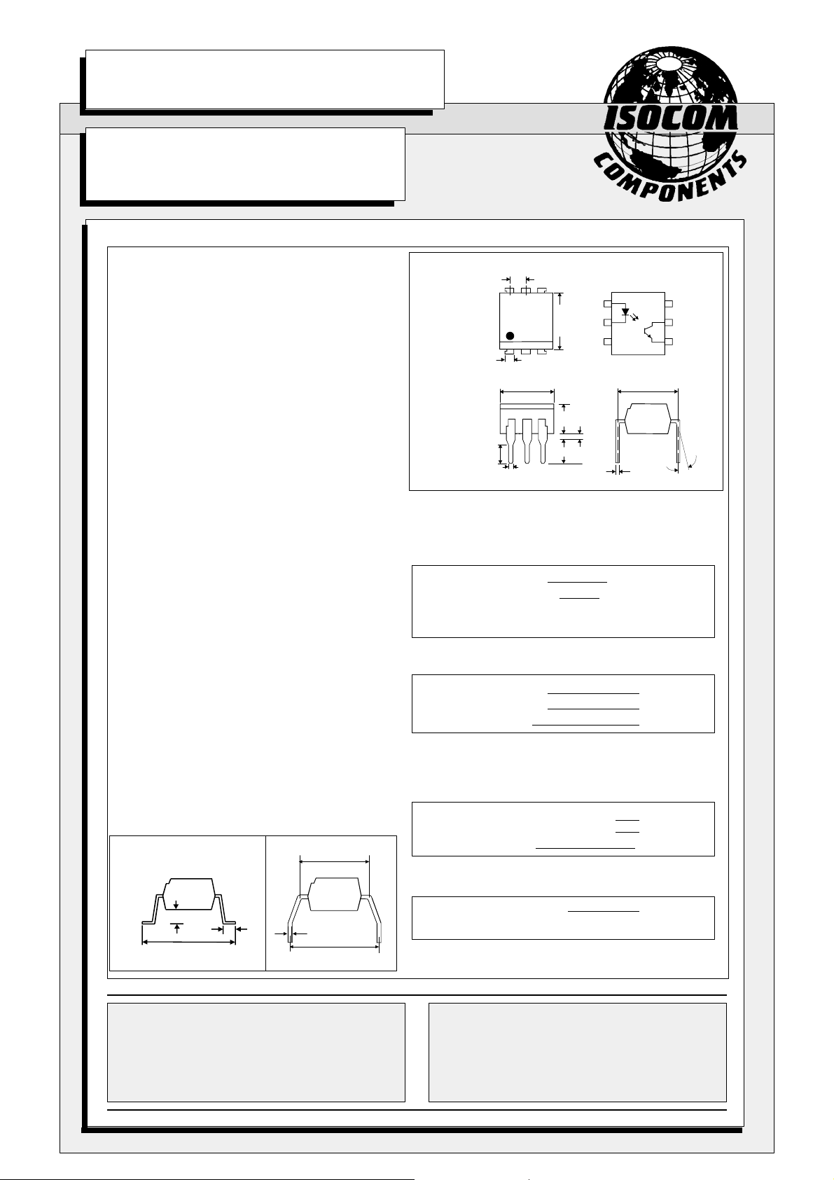
Dimensions in
mm
1
2 5
3 4
7.62
0.5
0.26
6
13°
Max
1.2
3.0
0.5
7.62
6.62
2.54
7.0
6.0
4.0
3.0
3.35
ABSOLUTE MAXIMUM RATINGS
(25°C unless otherwise specified)
Storage Temperature -55°C to + 150°C
)
Operating Temperature -55°C to + 100°C
Lead Soldering Temperature
(1/16 inch (1.6mm) from case for 10 secs) 260°C
INPUT DIODE
Forward Current 60mA
Reverse Voltage 6V
Power Dissipation 120mW
OPTION SM
SURFACE
MOUNT
0.6
0.1
10.46
9.86
1.25
0.75
OPTION G
7.62
0.26
10.16
ISOCOM COMPONENTS LTD
Unit 25B, Park View Road West,
Park View Industrial Estate, Brenda Road
Hartlepool, Cleveland, TS25 1YD
Tel: (01429) 863609 Fax :(01429) 863581
OUTPUT TRANSISTOR
Collector-emitter Voltage BV
Emitter-collector Voltage BV
Power Dissipation 160mW
CEO
ECO
70V
7V
POWER DISSIPATION
Total Power Dissipation 200mW
(derate linearly 2.94mW/°C above 25°C)
ISOCOM INC
1024 S. Greenville Ave, Suite 240,
Allen, TX 75002 USA
Tel: (214) 495-0755 Fax: (214) 495-0901
e-mail info@isocom.com
http://www.isocom.com
DA92586-AAS/A2
13/12/00
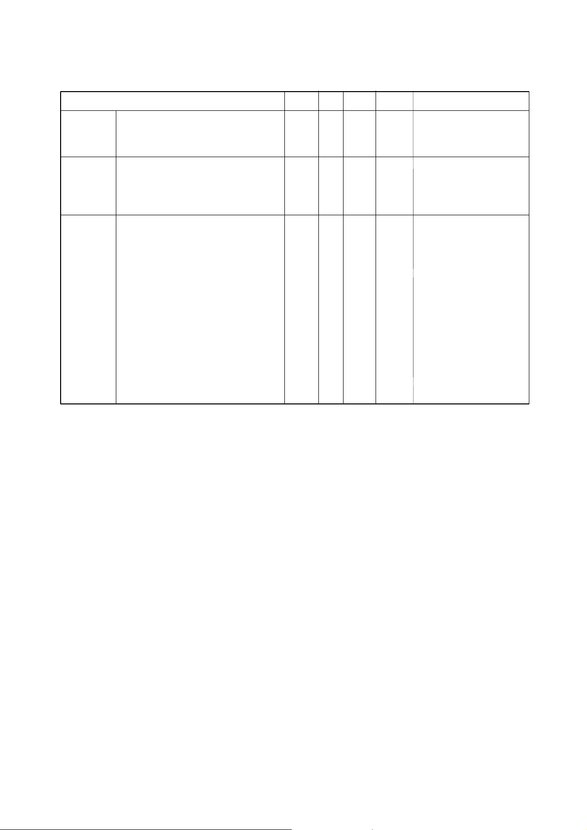
ELECTRICAL CHARACTERISTICS ( TA= 25°C Unless otherwise noted )
PARAMETER MIN TYP MAX UNITS TEST CONDITION
Input Forward Voltage (VF) 1.0 1.15 1.5 V IF = 10mA
Reverse Voltage (VR) 6 V IR = 10µA
Reverse Current (IR) 10 µA VR = 6V
Output Collector-emitter Breakdown (BV
( Note 2 )
Emitter-collector Breakdown (BV
Collector-emitter Dark Current (I
) 70 V IC = 1mA
CEO
) 6 V IE = 100µA
ECO
) 1.0 50 nA VCE = 10V
CEO
Coupled Output Collector Current IC (CTR)
( Note 2&3 )
MOC8106 5.0(50) 15(150) mA(%) 10mA IF , 10V V
MOC8107 10(100) 30(300) mA(%) 10mA IF , 10V V
MOC8108 25(250) 60(600) mA(%) 10mA IF , 10V V
Collector-emitter Saturation VoltageVCE
Input to Output Isolation Voltage V
Input-output Isolation Resistance R
(SAT)
5300 V
ISO
7500 V
5x10
ISO
0.15 0.4 V 5mA I
RMS
10
PK
Ω V
Turn-on Time ton 7.5 20 µs VCC = 10V ,
Turn-off Time toff 5.7 20 µs IC = 2mA, RL = 100Ω
Output Rise Time tr 3.2 µs
Output Fall Time tf 4.7 µs
Note 1 Measured with input leads shorted together and output leads shorted together.
Note 2 Special Selections are available on request. Please consult the factory.
Note 3 Production testing - limits verified with pulse test
, 0.5mA I
F
See note 1
See note 1
= 500V (note 1)
IO
CE
CE
CE
C
DA92586-AAS/A2
 Loading...