

ISOCOM COMPONENTS LTD
Unit 25B, Park View Road West,
Park View Industrial Estate, Brenda Road
Hartlepool, Cleveland, TS25 1YD
Tel: (01429) 863609 Fax :(01429) 863581
ISOCOM INC
720 E., Park Boulevard, Suite 104,
Plano, TX 75074 USA
Tel: (972) 423-5521
Fax: (972) 422-4549
3/10/97
DB92094-AAS/A2
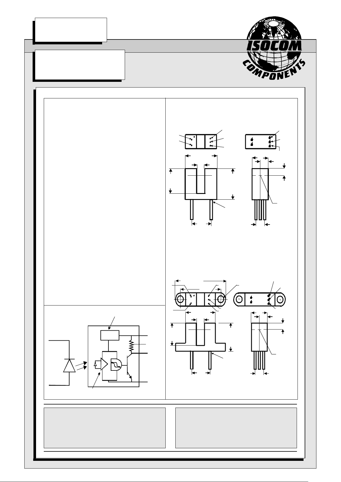
ISO - LOGIC INVERTE R
SCHMITT TRIGGER
INTERRUPTER SWITCH
ISTS972N, ISTS973N
ISTS972T, ISTS973T
OPTICAL
CENTRE
LINE
12.7
E
3.0
1
2
5
4
9.0
8.0
11.1
10.5
0.45
0.40
7.62
6.6
3.3
3.0
2.8
2.54
Dimensions in mm
3
1
2
pin 5 G
ND
pin 3 V
CC
pin 4 V
O
OPTICAL
CENTRE
LINE
12.7
E
3.0
1
2
5
4
9.0
8.0
11.1
10.5
0.45
0.40
7.62
6.6
3.3
3.0
2.8
2.54
3
1
2
pin 3 V
CC
pin 4 V
O
25.7
24.1
19.05
pin 5 G
ND
ISTS972N
ISTS973N
ISTS972T
ISTS973T
Voltage Regulator
4 Out
3 V
CC
5 G
ND
10kΩ
Amp
ISTS972
only
1
2
DESCRIPTION
The ISTS972 and ISTS973 series of
transmissive photointerrupters are single channel
switches consisting of a Gallium Arsenide
infrared emitting diode coupled to a high speed
integrated circuit detector. The output
incorporates a Schmitt trigger which provides
hysteresis for noise immunity and pulse shaping.
The gap in the plastic housing provides a means
of interrupting the signal with an opaque
material, switching the output from an 'ON' into
an 'OFF' state.
FEATURES
l Built in Schmitt trigger circuit
l Pull up resistor between V
CC
and output
(ISTS972)
l Open collector output (ISTS973)
l High sensitivity
l 3mm gap between LED and detector
l 1mm aperture over detector
APPLICATIONS
l Floppy disk drives, Copiers, Printers,
Facsimilies, VCR's, Cassette tape
Recorders, Automatic vending machines
DB92094-AAS/A2
PARAMETER MIN TYP MAX UNITS TEST CONDITION
Input Forward Voltage (VF) 1.1 1.7 V IF = 20mA
Reverse Voltage (VR)6VI
R
= 10µA
Reverse Current (IR)10µAV
R
= 3V
Detector Operating Voltage Range V
CC
4.75 5.25 V
Low Level Supply Current I
CCL
2.0 15 mA VCC= 5.25V, IF = 15mA
High Level Supply Current I
CCH
1.0 15 mA VCC= 5.25V, IF = 0mA
Low Level Output Voltage V
OL
0.4 V VCC= 4.75V, IF = 15mA
I
OL
= 12.8mA
High Level Output Voltage V
OH
ISTS972 2.4 V VCC= 4.75V, IF = 0mA
I
OH
= -800µA
High Level Output Current I
OH
ISTS973 10 0 µAV
CC
= 4.75V, IF = 0mA
V
OH
= 30V
Input Forward Threshold Current I
FT
15 mA VCC= 5V
Propagation Delay Time
to Logic High at Output t
PLH
5 µs
Propagation Delay Time VCC= 5V
to Logic Low at Output t
PHL
5 µsI
F
= 15mA
RL= 360Ω (ISTS973)
Rise Time tr 0.1 µsor
R
L
= 8TTL Loads
Fall Time tf 0.05 µs (ISTS972)
Note 1 Special Selections are available on request. Please consult the factory.
3/10/97
ELECTRICAL CHARACTERISTICS ( TA= 25°C Unless otherwise noted )
ABSOLUTE MAXIMUM RATINGS (25°C unless
otherwise specified)
Storage Temperature -40°C to +85°C
Operating Temperature -25°C to +85°C
Lead Soldering Temperature 260°C
(5 secs maximum)
INFRARED EMITTING DIODE
Power Dissipation 75 mW
Forward Current ( Continuous ) 50 mA
Forward Current ( Peak ) 1 A
(Pulse Width ≤ 100µs, Duty Ratio = 0.01)
Reverse Voltage 6V
PHOTO DETECTOR
Power Dissipation 250 mW
Output Current 50mA
Allowed Range V
35
(ISTS972) 0 to 17V
(ISTS973) 0 to 35V
Allowed Range V
45
(ISTS972) 0 to 17V
(ISTS973) 0 to 40V
DB92094-AAS/A2
3/10/97
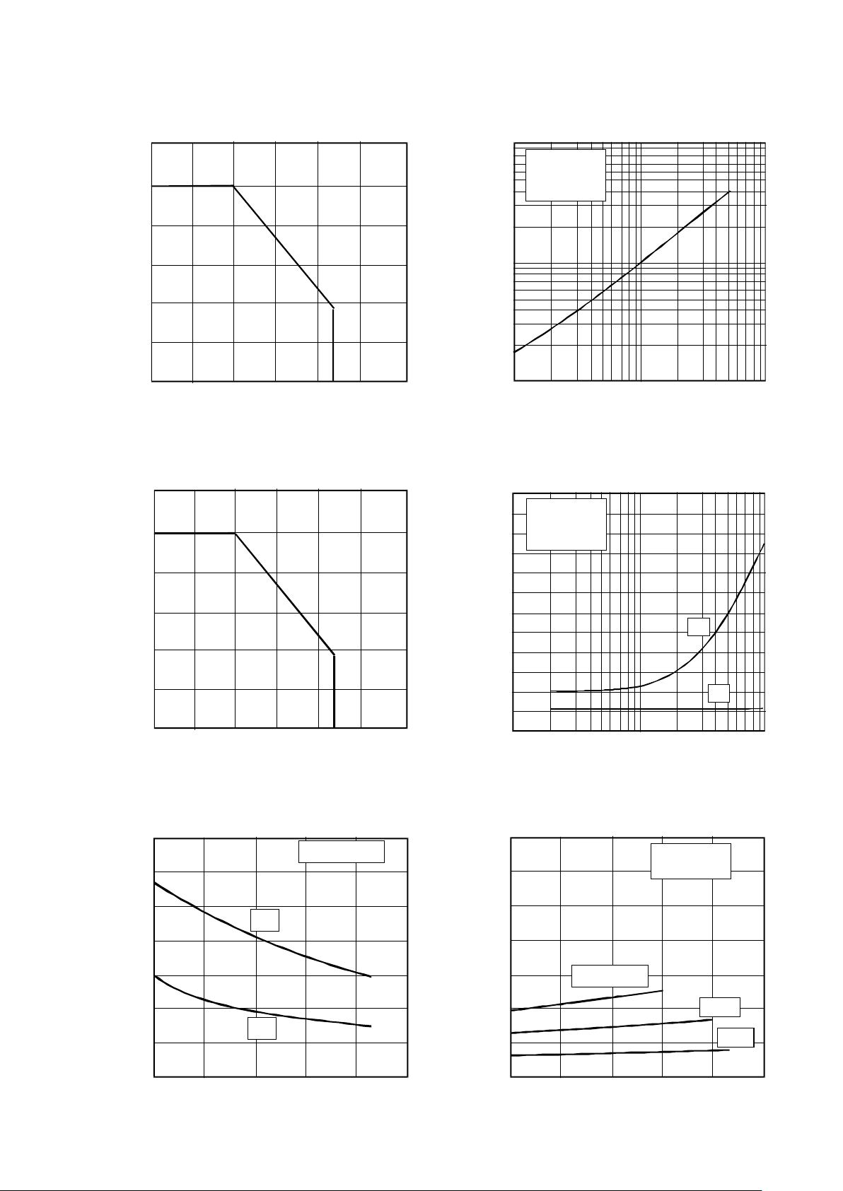
50
-25 0 25 50 75 100 125
Ambient temperature TA ( °C )
0
300
Collector power dissipation P
C
(mW)
Collector Power Dissipation vs. Ambient Temperature
0
1.0
2.0
3.0
VCC = 5.25V
Ambient temperature TA ( °C )
-25 0 25 50 75 100
-25 0 25 50 75 100
Ambient temperature TA ( °C )
Low level output voltage V
OL
( V )
Low Level Output Voltage vs.
Ambient Temperature
0
0.1
0.2
0.3
0.4
0.5
0.6
0.7
1
Low level output voltage V
OL
( V )
Low Level Output Voltage vs.
Low Level Output Current
Low level output current I
OL
( mA )
0.1
0.01
0.02
0.2
0.5
Supply Current vs.
Ambient Temperature
Supply current I
CC
(mA)
V
CC
= 4.75V
IF = 15mA
TA = 25°C
0.1 0.2 0.5 1 2 5 10
0
0.1
0.2
0.3
0.4
Rise time, fall time tr, tf (µs)
Rise Time, Fall Time vs. Load
Resistance
Load resistance RL ( kΩ)
0.5
Ambient temperature TA ( °C )
60
30
20
10
0
40
50
-25 0 25 50 75 100 125
Forward Current vs. Ambient Temperature
Forward current I
F
(mA)
100
150
200
250
1 10 50 100
0.05
V
CC
= 4.75V
IF = 15mA
TA = 25°C
0.6
I
CCH
I
CCL
V
CC
= 5.25V
IF = 15mA
IOL = 30mA
5mA
16mA
tf
tr
 Loading...