

ISOCOM ISTS822SS, ISTS822SD, ISTS822S, ISTS250, ISTS832SS Datasheet
...
ISOCOM COMPONENTS LTD
Unit 25B, Park View Road West,
Park View Industrial Estate, Brenda Road
Hartlepool, Cleveland, TS25 1YD
Tel: (01429) 863609 Fax :(01429) 863581
ISOCOM INC
720 E., Park Boulevard, Suite 104,
Plano, TX 75074 USA
Tel: (972) 423-5521
Fax: (972) 422-4549
24/9/97
DB92003-AAS/A1
TRANSMISSIVE OPTO-ELECTRONIC DUAL
CHANNEL SLOTTED INTERRUPTER
SWITCHES WITH TRANSISTOR SENSORS
ABSOLUTE MAXIMUM RATINGS
(25°C unless otherwise specified)
Storage Temperature -40°C to + 85°C
Operating Temperature -25°C to + 85°C
Lead Soldering Temperature
(1/16 inch (1.6mm) from case for 10 secs) 260°C
INPUT DIODE
Forward Current 50mA
Reverse Voltage 5V
Power Dissipation 75mW
OUTPUT TRANSISTOR
Collector-emitter Voltage BV
CEO
30V
Emitter-collector Voltage BV
ECO
5V
Collector Current I
C
20mA
Power Dissipation 75mW
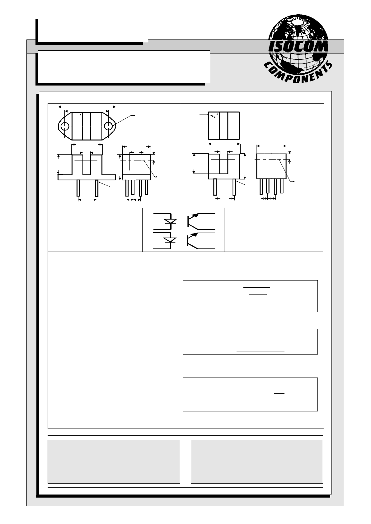
ISTS150, ISTS832S, ISTS832SD
ISTS250, ISTS822S, ISTS822SD
3.2
DIA 2
PLCS
ISTS250
ISTS822S
ISTS822SD
2.8
OPTICAL
CENTRE
LINE
2.54
0.45
0.40
7.62
E
DESCRIPTION
This series of photointerrupters are dual
channel switches consisting of two Gallium
Arsenide infrared emitting diodes and two NPN
silicon photo transistors mounted in a "side by
side" configuration on opposite sides of a 2.5mm
wide slot. Dual channels enable direction of
travel sensing. The transmissive housing reduces
possible interference from ambient light and
provides dust and dirt protection. In addition the
ISTS822S, ISTS832S have 0.25mm apertures in
front of the phototransistors, While the
ISTS822SD, ISTS832SD have the same sized
apertures in front of both emitters and
phototransistors
FEATURES
l Single or Double apertures for High Resolution
l 2.5mm Gap between LED and Detector
l Dual channels "side by side"
APPLICAT IO NS
l Copiers, Printers, Facsimilies, Record
Players, Cassette Decks, VCR's
ISTS150
ISTS832S
ISTS832SD
OPTICAL
CENTRE
LINE
1
Dimensions in mm
10.4
10.0
11.4
2.54
7.9
7.4
7.62
2.54 2.8
2.8
11.5
E
2.8
0.45
0.40
11.4
7.9
7.4
17.8
11.5
5.4
10.4
10.0
2.54
24.2
1
2
3
4
8
7
6
5
DB92003-AAS/A1
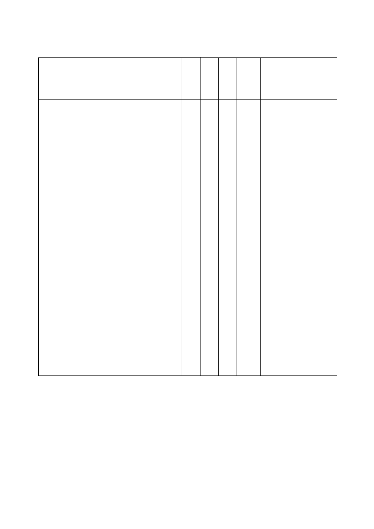
PARAMETER MIN TYP MAX UNITS TEST CONDITION
Input Forward Voltage (VF) 1.2 1.6 V IF = 20mA
Reverse Voltage (VR)3VI
R
= 10µA
Reverse Current (IR)10µAV
R
= 3V
Output Collector-emitter Breakdown (BV
CEO
)30 V IC = 1mA
( Note 1 )
Emitter-collector Breakdown (BV
ECO
) 5 V IE = 100µA
Collector-emitter Dark Current (I
CEO
) 100 nA VCE = 10V
Coupled On-State Collector Current IC (
ON
)
( Note 1 )
ISTS150, ISTS250 250 µA 20mA I
F
, 10V V
CE
( no apertures )
ISTS822S, ISTS832S 250 µA 20mA IF , 10V V
CE
(0.25mm apertures phototransistors only)
ISTS822SD, ISTS832SD 100 µA 20mA I
F
, 10V V
CE
( 0.25mm apertures in front of both -
- emitters and phototransistors )
Collector-emitter Saturation VoltageV
CE(SAT)
ISTS150, ISTS250 0.4 V 20mA I
F
, 125µA I
C
ISTS822S, ISTS832S 0.4 V 20mA I
F
, 125µA I
C
ISTS822SD, ISTS832SD 0.4 V 20mA I
F
, 50µA I
C
Rise Time tr 6 µsV
CC
= 5V,
Fall Time tf 6 µsI
F
= 20mA, RL= 100Ω
Note 1 Special Selections are available on request. Please consult the factory.
24/9/97
ELECTRICAL CHARACTERISTICS ( TA= 25°C Unless otherwise noted )
 Loading...