

ISOCOM ISQ201 User Manual
12/3/03
查询IS201供应商
IS201, IS202, IS203, IS204,
ISD201, ISD202, ISD203, ISD204,
ISQ201, ISQ202, ISQ203, ISQ204
HIGH DENSITY
PHOTOTRANSISTOR OPTICALLY
COUPLED ISOLATORS
APPROVALS
ll UL recognised, File No. E91231
'X' SPECIFICATION APPROVALS
l VDE 0884 in 3 available lead form : -
- STD
- G form
- SMD approved to CECC 00802
l IS20* Certified to EN60950 by the
following Test Bodies :Nemko - Certificate No. P01102464
Fimko - Certificate No. FI18166
Semko - Reference No. 0202037/01-22
Demko - Certificate No. 311158-01
l BSI approved - Certificate No. 8001
DESCRIPTION
The IS20*, ISD20*, ISQ20* series of optically
coupled isolators consist of infrared light
emitting diodes and NPN silicon photo
transistors in space efficient dual in line plastic
packages.
FEATURES
l Options :-
10mm lead spread - add G after part no.
Surface mount - add SM after part no.
Tape&reel - add SMT&R after part no.
l High Isolation Voltage (5.3kV
l High BV
l All electrical parameter 100% tested
l Custom electrical selections available
(70V min)
CEO
RMS
,7.5kV
PK
APPLICATIONS
l Computer terminals
l Industrial systems controllers
l Signal transmission between systems of
different potentials and impedances
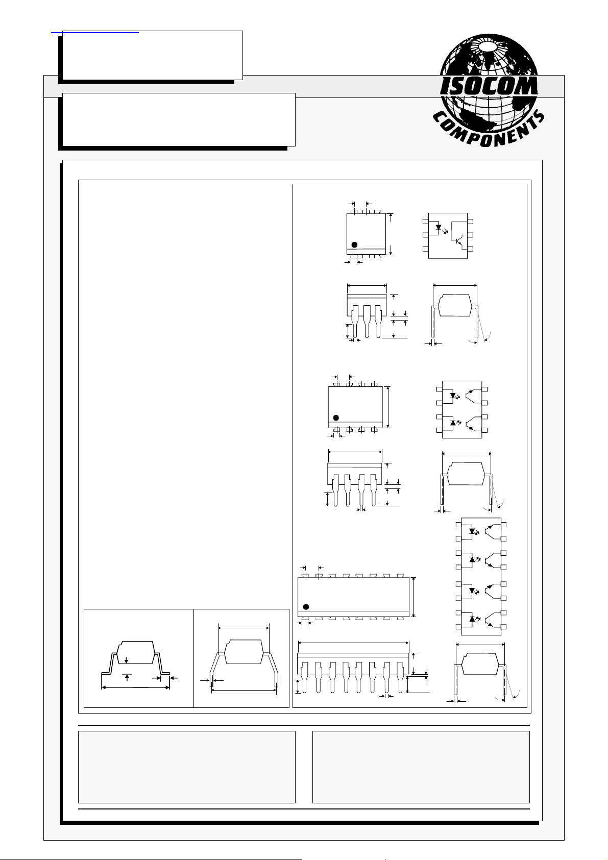
OPTION SM
SURFACE MOUNT
0.6
0.1
10.46
9.86
1.25
0.75
OPTION G
7.62
0.26
10.16
)
IS201
IS202
IS203
IS204
ISD201
ISD202
ISD203
ISD204
1.2
3.0
ISQ201
ISQ202
ISQ203
ISQ204
1.2
3.0
1.2
3.0
2.54
10.16
9.16
20.32
19.32
0.5
7.62
6.62
2.54
0.5
2.54
3.35
7.0
6.0
3.35
7.0
6.0
4.0
3.0
0.5
1
2 5
3 4
4.0
3.0
0.5
1
2
3
4 5
0.5
7.0
6.0
4.0
3.0
0.5
3.35
Dimensions in mm
6
7.62
13°
Max
0.26
8
7
6
7.62
13°
Max
0.26
1
2
3
4
5
6
7
8
7.62
0.26
16
15
14
13
12
11
10
9
13°
Max
ISOCOM COMPONENTS LTD
Unit 25B, Park View Road West,
Park View Industrial Estate, Brenda Road
Hartlepool, Cleveland, TS25 1YD
Tel: (01429) 863609 Fax :(01429) 863581
ISOCOM INC
1024 S. Greenville Ave, Suite 240,
Allen, TX 75002 USA
Tel: (214) 495-0755 Fax: (214) 495-0901
e-mail info@isocom.com
http://www.isocom.com
DB91021m-AAS/A4
12/3/03
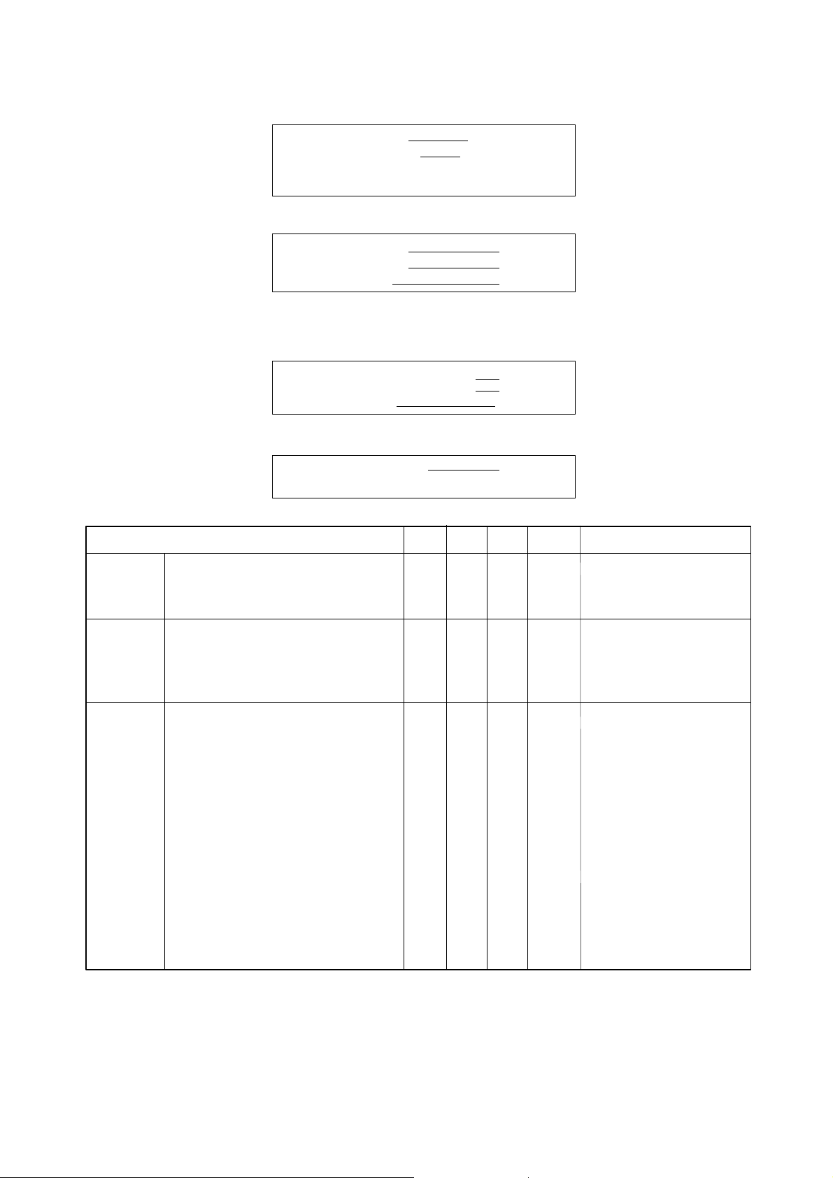
ABSOLUTE MAXIMUM RATINGS
(25°C unless otherwise specified)
Storage Temperature -40°C to + 125°C
Operating Temperature -25°C to + 100°C
Lead Soldering Temperature
(1/16 inch (1.6mm) from case for 10 secs) 260°C
INPUT DIODE
Forward Current 50mA
Reverse Voltage 6V
Power Dissipation 70mW
OUTPUT TRANSISTOR
Collector-emitter Voltage BV
Emitter-collector Voltage BV
Power Dissipation 150mW
CEO
ECO
70V
6V
POWER DISSIPATION
Total Power Dissipation 170mW
(derate linearly 2.67mW/°C above 25°C)
ELECTRICAL CHARACTERISTICS ( TA = 25°C Unless otherwise noted )
PARAMETER MIN TYP MAX UNITS TEST CONDITION
Input Forward Voltage (VF) 1.2 1.65 V IF = 50mA
Reverse Current (IR) 10 µA VR = 4V
Output Collector-emitter Breakdown (BV
( Note 2 )
Emitter-collector Breakdown (BV
Collector-emitter Dark Current (I
) 70 V IC = 1mA
CEO
) 6 V IE = 100µA
ECO
) 50 nA VCE = 10V
CEO
Coupled Current Transfer Ratio (CTR) (Note 2)
IS201, ISD201, ISQ201 75 % 10mA IF , 10V V
IS201, ISD201, ISQ201 10 % 1mA IF , 10V V
IS202, ISD202, ISQ202 125 250 % 10mA IF , 10V V
IS202, ISD202, ISQ202 30 % 1mA IF , 10V V
IS203, ISD203, ISQ203 225 450 % 10mA IF , 10V V
IS203, ISD203, ISQ203 50 % 1mA IF , 10V V
IS204, ISD204, ISQ204 200 400 % 10mA IF , 10V V
IS204, ISD204, ISQ204 100 % 1mA IF , 10V V
Collector-emitter Saturation Voltage V
Input to Output Isolation Voltage V
Input-output Isolation Resistance R
Output Turn on Time t
Output Turn off Time t
ON
OFF
CE(SAT)
5300 V
ISO
7500 V
5x10
ISO
0.2 0.4 V 10mA IF , 2mA I
RMS
10
PK
Ω V
See note 1
See note 1
IO
3.0 µs IF = 10mA
2.5 µs V
CE
CE
CE
CE
CE
CE
CE
CE
CE
C
= 500V (note 1)
= 5V, RL = 75Ω
Note 1 Measured with input leads shorted together and output leads shorted together.
Note 2 Special Selections are available on request. Please consult the factory.
DB91021m-AAS/A4
 Loading...