

ISOCOM IS733 Datasheet
19/4/99
IS733
A.C. INPUT PHOTOTRANSISTOR
OPTICALLY COUPLED
ISOLATORS
APPROVALS
l UL recognised, File No. E91231
'X' SPECIFICATION APPROVALS
l VDE 0884 approval pending
l EN60950 approval pending
DESCRIPTION
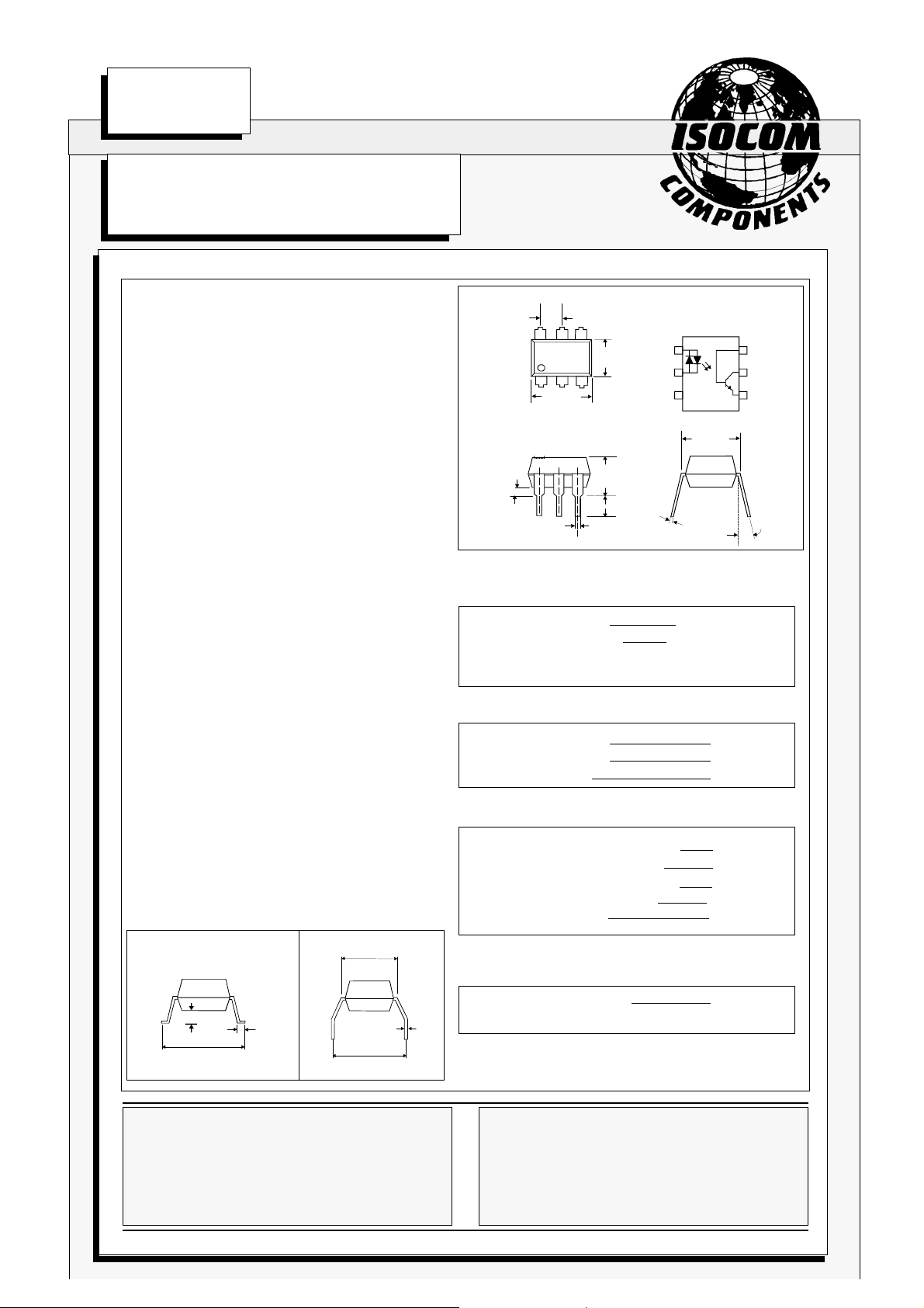
The IS733 optically coupled isolator consists of
two infrared light emitting diodes connected in
inverse parallel and NPN silicon photo transistor
in a standard 6 pin dual in line plastic package.
FEATURES
l Options :-
10mm lead spread - add G after part no.
Surface mount - add SM after part no.
Tape&reel - add SMT&R after part no.
l High Isolation Voltage (5.3kV
l AC or polarity insensitive input
l All electrical parameters 100% tested
l Custom electrical selections available
RMS
,7.5kV
PK
APPLICATIONS
l Computer terminals
l Industrial systems controllers
l Telephone sets, Telephone exchangers
l Signal transmission between systems of
different potentials and impedances
OPTION SM
SURFACE MOUNT
OPTION G
8.3 max
2.54
Dimensions in mm
7.0
6.0
7.62
max.
8.3 max.
5.1
0.5
min.
max.
3.9
3.1
0.48
0.25
ABSOLUTE MAXIMUM RATINGS
(25°C unless otherwise specified)
Storage Temperature -55°C to + 150°C
Operating Temperature -55°C to + 100°C
Lead Soldering Temperature
(1/16 inch (1.6mm) from case for 10 secs) 260°C
)
INPUT DIODE
Forward Current ±50mA
Peak Forward Current ±1A
Power Dissipation 70mW
OUTPUT TRANSISTOR
Collector-emitter Voltage BV
Collector-base Voltage BV
Emitter-collector Voltage BV
Emitter-base Voltage BV
Power Dissipation 150mW
CEO
CBO
ECO
EBO
POWER DISSIPATION
15°
Max
35V
35V
6V
6V
1.2
0.6
10.2
9.5
1.4
0.9
0.26
10.16
ISOCOM COMPONENTS LTD
Unit 25B, Park View Road West,
Park View Industrial Estate, Brenda Road
Hartlepool, TS25 1YD England Tel: (01429)863609
Fax : (01429) 863581 e-mail sales@isocom.co.uk
http://www.isocom.com
Total Power Dissipation 170mW
(derate linearly 2.27mW/°C above 25°C)
ISOCOM INC
1024 S. Greenville Ave, Suite 240,
Allen, TX 75002 USA
Tel: (214) 495-0755 Fax: (214) 495-0901
e-mail info@isocom.com
http://www.isocom.com
DB91060-AAS/A1
19/4/99
ELECTRICAL CHARACTERISTICS ( TA = 25°C Unless otherwise noted )
PARAMETER MIN TYP MAX UNITS TEST CONDITION
Input Forward Voltage (VF) 1.2 1.4 V IF = ±20mA
Output Collector-emitter Breakdown (BV
( note 2 )
Collector-base Breakdown (BV
Emitter-base Breakdown (BV
Emitter-collector Breakdown (BV
Collector-emitter Dark Current (I
) 35 V IC = 1mA
CEO
) 35 V IC = 100µA
CBO
) 6 V IE = 100µA
EBO
) 6 V IE = 100µA
ECO
) 100 nA VCE = 20V
CEO
Coupled Current Transfer Ratio (CTR) (note 2 ) 15 300 % ±1mAIF , 5V V
Collector-emitter Saturation VoltageV
Input to Output Isolation Voltage V
Input-output Isolation Resistance R
CE(SAT)
ISO
ISO
5300 V
7500 V
10
5x10
0.2 V ±20mAIF , 1mAI
RMS
PK
Ω V
See note 1
See note 1
= 500V (note 1)
IO
Output Rise Time tr 4 18 µs VCE = 2V ,
Output Fall Time tf 3 18 µs IC= 2mA, RL = 100Ω
CE
C
Note 1 Measured with input leads shorted together and output leads shorted together.
Note 2 Special Selections are available on request. Please consult the factory.
DB91060-AAS/A1
 Loading...