

ISOCOM IS355 Datasheet
ISOCOM COMPONENTS LTD
Unit 25B, Park View Road West,
Park View Industrial Estate, Brenda Road
Hartlepool, Cleveland, TS25 1YD
Tel: (01429) 863609 Fax :(01429) 863581
HIGH DENSITY MOUNTING
PHOTODARLINGTON
OPTICALLY COUPLED ISOLATORS
DESCRIPTION
The IS355 is an optically coupled isolator
consisting of an infrared light emitting diode and
NPN silicon photodarlington in a space efficient
dual in line plastic package.
FEATURES
l Marked as FPD1.
l Current Transfer Ratio MIN. 600%
l Isolation Voltage (3.75kV
RMS
,5.3kV
PK
)
l All electrical parameters 100% tested
l Drop in replacement for Sharp PC355
APPLICATIONS
l Computer terminals
l Industrial systems controllers
l Measuring instruments
l Signal transmission between systems of
different potentials and impedances
ISOCOM INC
1024 S. Greenville Ave, Suite 240,
Allen, TX 75002 USA
Tel: (214) 495-0755 Fax: (214) 495-0901
e-mail info@isocom.com
http://www.isocom.com
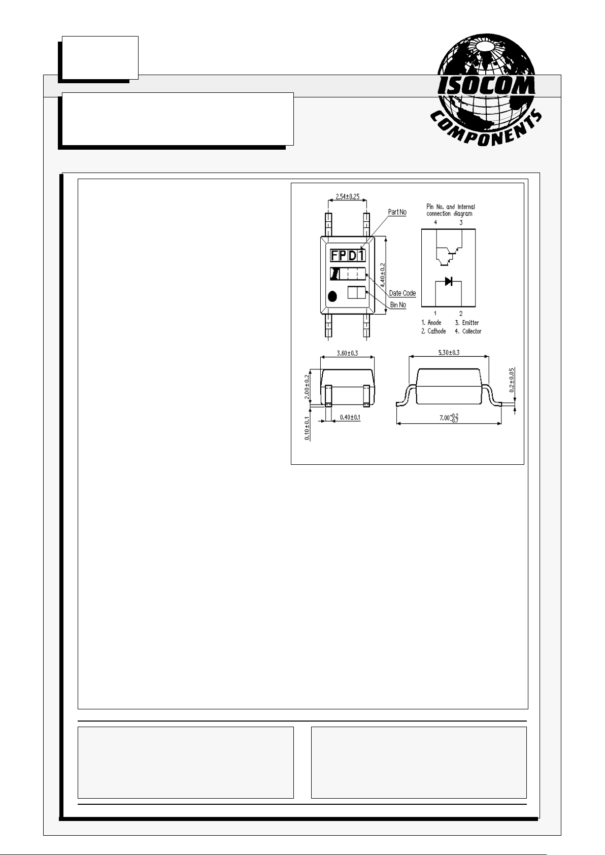
IS355
DB92859l-AAS/A3
22/4/02
Dimensions in mm

PARAMETER MIN TYP MAX UNITS TEST CONDITION
Input Forward Voltage (VF) 1.2 1.4 V IF = 20mA
Reverse Voltage (VR) 5 V IR = 10µA
Reverse Current (IR) 10 µA VR = 4V
Output Collector-emitter Breakdown (BV
CEO
) 35 V IC = 0.1mA
Emitter-collector Breakdown (BV
ECO
) 6 V IE = 10uA
Collector-emitter Dark Current (I
CEO
) 1 uA VCE = 10V
Coupled Current Transfer Ratio (CTR) 600 7500 % 1mA IF , 2V V
CE
Collector-emitter Saturation VoltageVCE
(SAT)
1 V 20mA IF , 1mA I
C
Input to Output Isolation Voltage V
ISO
3750 V
RMS
See note 1
5300 V
PK
See note 1
Input-output Isolation Resistance R
ISO
5x10
10
Ω V
IO
= 500V (note 1)
Output Rise Time tr 4 18 µs VCE = 2V ,
Output Fall Time tf 3 18 µs IC = 2mA, RL = 100Ω
ELECTRICAL CHARACTERISTICS ( TA = 25°C Unless otherwise noted )
ABSOLUTE MAXIMUM RATINGS
(25°C unless otherwise specified)
Storage Temperature -55°C to + 150°C
Operating Temperature -55°C to + 100°C
Lead Soldering Temperature
(1/16 inch (1.6mm) from case for 10 secs) 260°C
INPUT DIODE
Forward Current 50mA
Reverse Voltage 6V
Power Dissipation 70mW
OUTPUT TRANSISTOR
Collector-emitter Voltage BV
CEO
35V
Emitter-collector Voltage BV
ECO
6V
Power Dissipation 150mW
POWER DISSIPATION
Total Power Dissipation 170mW
(derate linearly 2.26mW/°C above 25°C)
Note 1 Measured with input leads shorted together and output leads shorted together.
DB92859l-AAS/A3
22/4/02
 Loading...