

ISOCM ICPL2611 Datasheet
ICPL2611
13/12/00
HIGH CMR, HIGH SPEED OPTO
ISOLATOR
DESCRIPTION
The ICPL 2611 consists of a GaAsP emitting diode and a
unique integrated detector. The photons are detected by a
photodiode and then amplified by a high gain linear
amplifier that drives a logic gate with a strobable output.
This output features a Schottky clamped open collector
output transistor. The circuit is temperature, current and
voltage compensated. This unique isolator design
provides maximum DC and AC circuit isolation between
input and output while achieving LSTTL/TTL circuit
compatibility. The isolator operational parameters are
guaranteed from 0°C to 70°C, such that a minimum input
current of 5 mA will sink an eight gate fan-out (13mA)
at the output with 5 volt Vcc supplied to the detector.
This isolation and coupling is achieved with a typical
propagation delay of 39ns. The enable input provides
gating of the detector with input sinking and sourcing
requirements compatible with LSTTL/TTL interfacing
and a propagation delay of 35ns typical.
FEATURES
l LSTTL/TTL Compatible
l High Speed
l Low Input Current Required
l Guaranteed Performance over Temperature
l 2500 V
l Internal Shield for High Common Mode Rejection
Withstand Test Voltage (1 Minute)
RMS
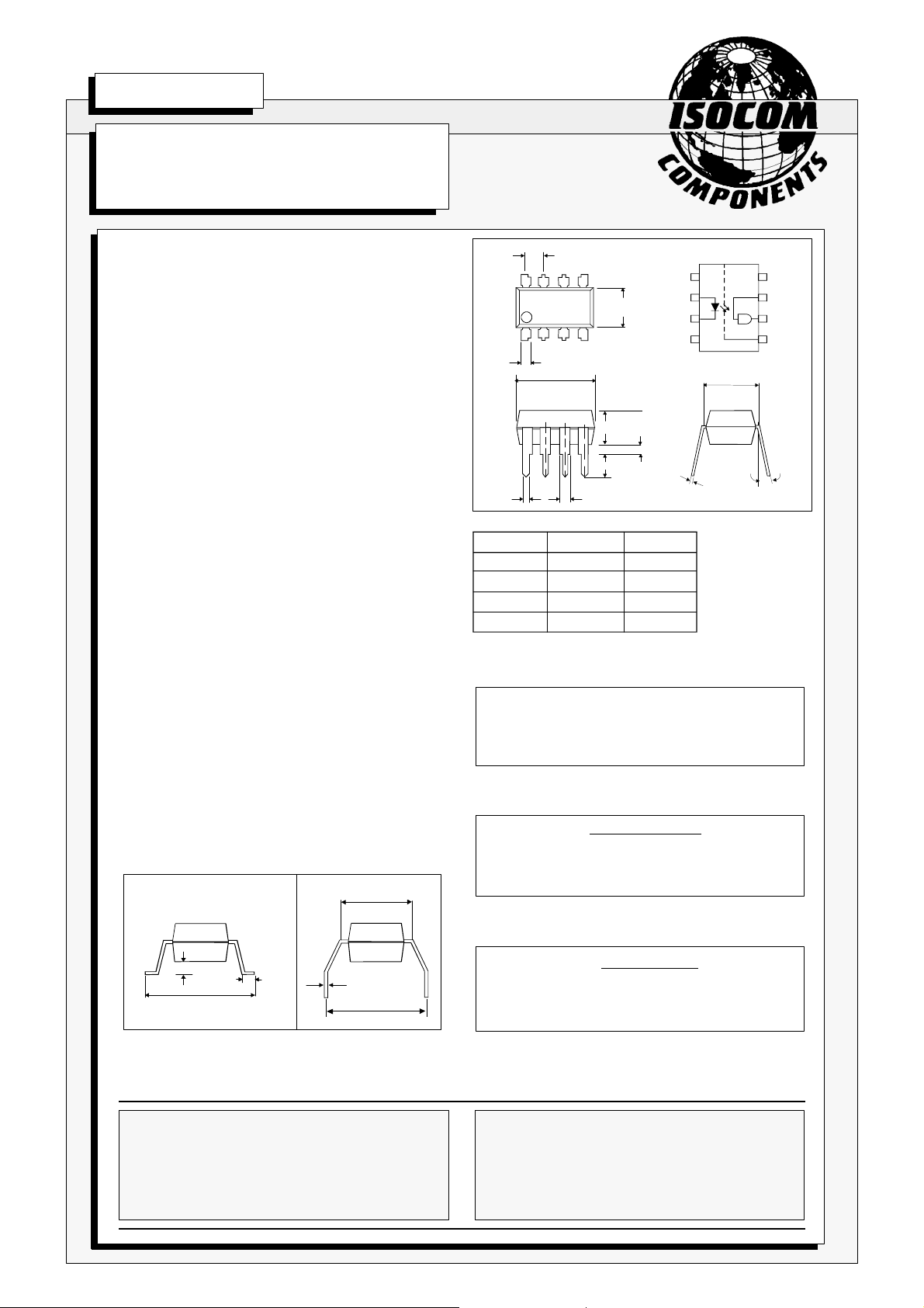
2.54
Dimensions in mm
1
2
3
*
4
* ICPL2601 NOISE SHIELD
7.62
1.3
6.9
6.3
9.7
9.1
4.0
3.6
0.5
0.3
0.5
3.3
1.3
TRUTH TABLE
INPUT ENABLE OUTPUT
H H L
L H H
H L H
L L H
ABSOLUTE MAXIMUM RATINGS
(25 °C unless otherwise noted)
Storage Temperature ___________ -55 to +1250C
Operating Temperature _________ -0°C to +700C
Lead Solder Temperature ________ 2600C for 10secs
(1.6mm below the seating plate)
INPUT DIODE
A 0.1µF bypass
capacitor must be
connected between
pins 8 and 5 ( See
note 1)
V
15°
Max
CC
8
7
6
5
GND
OPTION SM
SURFACE MOUNT
1.2
0.6
1.4
0.9
OPTION G
7.62
0.3
10.2
9.5
10.16
ISOCOM COMPONENTS LTD
Unit 25B, Park View Road West,
Park View Industrial Estate, Brenda Road
Hartlepool, Cleveland, TS25 1YD
Tel: (01429) 863609 Fax: (01429) 863581
Forward Current 20mA (2)
Reverse Voltage ________________ 5V
Enable Voltage _________________5.5V
(Not to exceed Vcc by more that 500mV)
OUTPUT PHOTOTRANSISTOR
Supply VoltageVcc 7V (1 Min Max)
Current - lo _____________________ 25mA
Collector Power Dissipation _______40mW
Collector Voltage - Vo ____________7V
All electrical parameters are 100 % tested
Specifications are guaranteed to a cumulative 0.65%
AQL
ISOCOM INC
1024 S. Greenville Ave, Suite 240,
Allen, TX 75002 USA
Tel: (214) 495-0755 Fax: (214) 495-0901
e-mail info@isocom.com
http://www.isocom.com
DA91019-AAS/01

ELECTRICAL CHARACTERISTICS (Over recommended temperature 0°C to70°C unless specified)
13/12/00
PARAMETER
High Level Output Current I
Low Level Output Voltage V
High Level Enable Current I
Low Level Enable Current I
High Level Supply Current I
Low Level Supply Current I
OH
OL
EH
EL
CCH
CCL
Input - Output Insulation Leakage
Current - I
IO
Withstand Insulation Test Voltage
V
ISO
Resistance - R
Capacitance - C
Input Forward Voltage - V
IO
IO
F
Input Reverse Breakdown Voltage
- B
VR
Input Capacitance - C
IN
Current Transfer Ratio - CTR
High Level Enable Voltage - V
Low Level Enable Voltage - V
Input Diode Temperature
Coefficient
EH
EL
∆VF
∆TA
MIN
2500
5
2.0
TYP*
7
0.4
-1.0
-1.6
10
15
10
0.6
1.5
60
700
-1.4
12
MAX UNITS
0.6
µA
V
250
mA
mA
-2.0
mA
15
mA
19
µA
1.0
V
ohm
pF
1.75
V
V
pF
%
V
V
0.8
RMS
TEST CONDITIONS
Vcc =5.5V, Vo = 5.5V. IF = 250µA VE= 2.0V
Vcc =5.5V, IF = 5mA, VE = 2.0V
I0L (sinking) = 13mA
Vcc =5.5V, VE = 2.0V
Vcc =5.5V, VE = 0.5V
Vcc =5.5V, IF = 0, VE = 0.5V
Vcc =5.5V, IF =10 mA, VE = 0.5V
Relative Humidity = 45%
TA = 25 °C, t = 5s, VI0 = 3000 V DC mA,
RH < 50%, TA = 25°C, t = 1 Min
VI0 = 500V, t = 5s, TA = 25 °C
f = 1MHz, TA = 25 °C
IF = 10mA, TA = 25°C
IR = 10 µA, TA = 25°C
VF = 0, f, = 1MHz
IF= 5mA, RL= 100Ω
Vcc =5.5V, IF =10 mA
Vcc =5.5V, IF =10 mA
lF = 10mA,
FIG NOTE
3
3
3
3
12
11
11
*All typicals are at V
1 Bypassing of the power supply line is required, with a 0.01 µ F ceramic disc capacitor adjacent to
each isolator. The power supply bus for the isolator(s) should be seperate from the bus for any
active loads. Otherwise a larger value of bypass capacitor (up to 0.1 µ F)may be needed to supress
regenerative feedback via the power supply.
2 Peaking circuits may produce transient input currents up to 50mA, 50ns maximum pulse width,
provided average current does not exceed 20mA
3 Device considered a two terminal device; pins 1, 2, 3, and 4 shorted together, and pins 5, 6, 7
and 8 shorted together.
4 The t
input pulse to the 1.5V point on the trailing edge of the output pulse.
5 The t
input pulse to 1.5V point on the leading edge of the output pulse.
6 The t
input pulse to the 1.5V point on the trailing edge of the output pulse.
7 The t
input pulse to the 1.5V point on the leading edge of the output pulse.
8 CMH is the maximum tolerable rate of rise of the common mode voltage to assure that the output
will remain in a high logic state (ie Vout> 2.0V).
9 CML is the maximum tolerable rate of fall of the common mode voltage to assure that the output
will remain in a low logic state (ie Vout< 0.8V)
10 For sinusoidal voltages dvCM = π fCMVCM(p-p)
11 No external pull up is required for a high logic state on the enable input.
12 DC current transfer ratio is defined as the ratio of the output collector current to the forward bias input
current times 100%.
= 5V, T
CC
propagation delay is measured from the 3.75 mA point on the trailing edge of the
PLH
propagation delay is measured from the 3.75mA point on the leading edge of the
PHL
enable propagation delay is measured from the 1.5V point of the trailing edge of the
ELH
enable propagation delay is measured from the 1.5V point on the leading edge of the
EHL
= 25°C
A
( )
dt max
DA91019-AAS/02
 Loading...