

7/12/00
DB91077m-AAS/A1
'X' SPECIFICATION APPROVALS
ll VDE 0884 in 3 available lead forms : -
- STD
- G form
- SMD approved to CECC 00802
DESCRIPTION
The H11D series of optically coupled isolators
consist of infrared light emitting diode and
NPN silicon photo transistor in a standard 6 pin
dual in line plastic package.
FEATURES
l Options :-
10mm lead spread - add G after part no.
Surface mount - add SM after part no.
Tape&reel - add SMT&R after part no.
l High Isolation Voltage (5.3kV
RMS
,7.5kV
PK
)
l High BV
CER
( 300V - H11D1, H11D2 )
( 200V - H11D3, H11D4 )
l All electrical parameters 100% tested
l Custom electrical selections available
APPLICATIONS
l DC motor controllers
l Industrial systems controllers
l Measuring instruments
l Signal transmission between systems of
different potentials and impedances
H11D1X, H11D2X, H11D3X, H11D4X
H11D1, H11D2, H11D3, H11D4
HIGH VOLTAGE OPTICALLY
COUPLED ISOLATOR
PHOTOTRANSISTOR OUTPUT
ABSOLUTE MAXIMUM RATINGS
(25°C unless otherwise specified)
Storage Temperature -55°C to + 150°C
Operating Temperature -55°C to + 100°C
Lead Soldering Temperature
(1/16 inch (1.6mm) from case for 10 secs) 260°C
INPUT DIODE
Forward Current 60mA
Reverse Voltage 6V
Power Dissipation 100mW
OUTPUT TRANSISTOR
Collector-emitter Voltage BV
CER
(RBE= 1MΩ )
H11D1, H11D2 300V
H11D3, H11D4 200V
Collector-base Voltage BV
CBO
H11D1, H11D2 300V
H11D3, H11D4 200V
Emitter-collector Voltage BV
ECO
6V
Power Dissipation 300mW
POWER DISSIPATION
Total Power Dissipation 260mW
(derate linearly 2.67mW/°C above 25°C)
0.26
0.5
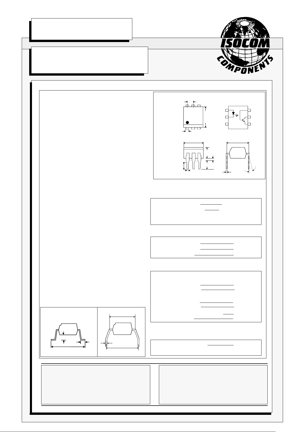
Dimensions in
mm
7.0
6.0
1.2
7.62
3.0
13°
Max
3.35
4.0
3.0
2.54
7.62
6.62
0.5
1
3 4
6
2 5
OPTION G
7.62
SURFACE MOUNT
OPTION SM
10.16
0.26
ISOCOM INC
1024 S. Greenville Ave, Suite 240,
Allen, TX 75002 USA
Tel: (214) 495-0755 Fax: (214) 495-0901
e-mail info@isocom.com
http://www.isocom.com
ISOCOM COMPONENTS LTD
Unit 25B, Park View Road West,
Park View Industrial Estate, Brenda Road
Hartlepool, TS25 1YD England Tel: (01429)863609
Fax : (01429) 863581 e-mail sales@isocom.co.uk
http://www.isocom.com
10.46
9.86
0.6
0.1
1.25
0.75
PARAMETER MIN TYP MAX UNITS TEST CONDITION
Input Forward Voltage (VF) 1.2 1.5 V IF = 10mA
Reverse Voltage (VR) 6 V IR = 10µA
Reverse Current (IR) 10 µA VR = 6V
Output Collector-emitter Breakdown (BV
CER
)
H11D1, H11D2 300 V IC = 1mA, RBE = 1MΩ
H11D3, H11D4 200 V ( note 2 )
Collector-base Breakdown (BV
CBO
)
H11D1, H11D2 300 V IC = 100µA
H11D3, H11D4 200 V
Emitter-collector Breakdown (BV
ECO
) 6 V IE = 100µA
Collector-emitter Dark Current (I
CER
)
H11D1, H11D2 100 nA VCE = 200V,RBE=1MΩ
250 µA VCE= 200V,RBE=1MΩ,
TA=100°C
H11D3, H11D4 100 nA VCE = 100V,RBE=1MΩ
250 µA VCE= 100V,RBE=1MΩ,
TA=100°C
Coupled Current Transfer Ratio (CTR) 20 % 10mA IF , 10V V
CE
,
RBE = 1MΩ
Collector-emitter Saturation VoltageV
CE(SAT)
0.4 V 10mA IF , 0.5mA IC ,
RBE = 1MΩ
Input to Output Isolation Voltage V
ISO
5300 V
RMS
See note 1
7500 V
PK
See note 1
Input-output Isolation Resistance R
ISO
5x10
10
Ω V
IO
= 500V (note 1)
Turn-on Time ton 5 µs VCC = 10V, IC= 2mA,
Turn-off Time toff 5 µs RL = 100Ω , fig 1
Note 1 Measured with input leads shorted together and output leads shorted together.
Note 2 Special Selections are available on request. Please consult the factory.
7/12/00
ELECTRICAL CHARACTERISTICS ( TA= 25°C Unless otherwise noted )
Output
Output
RL = 100Ω
Input
10%
90%
90%
10%
t
on
t
r
FIG 1
V
CC
t
off
t
f
DB91077m-AAS/A1

7/12/00
100
Ambient temperature TA ( °C )
300
0
400
Ambient temperature TA ( °C )
Collector power dissipation P
C
(mW)
60
30
20
10
40
50
-30 0 25 50 75 100 125
Collector Power Dissipation vs. Ambient Temperature
Forward Current vs. Ambient Temperature
200
Forward current I
F
(mA)
70
80
-30 0 25 50 75 100 125
0
0.4
0.6
0.8
1.0
1.2
0.2
1.4
Relative current transfer ratio
Relative Current Transfer Ratio
vs. Ambient Temperature
1 2 5 10 20 50
1.0
10
Relative current transfer ratio
Forward current IF (mA)
0.1
0.01
0.8
1.0
-30 0 25 50 75 100
Ambient temperature TA ( °C )
0
100
200
300
400
500
600
700
0.1 0.2 0.5 1 2 5 10 20 50
0.9
1.1
1.3
1.2
1.4
Forward current IF (mA)
Forward voltage V
F
(V)
VCE = 10V
RBE = 1MΩ
TA = 25°C
Relative Current Transfer Ratio vs.
Forward Current ( normalised to 10mA IF )
1.6
1.8
2.0
2.2
2.4
-30 0 25 50 75 100
Ambient temperature TA ( °C )
800
Normalised to VCE = 10V ,
IF = 10mA , RBE = 1MΩ ,
TA = 25°C
IF = 20mA
IF = 10mA
IF = 5mA
Collector-base current I
CBO
(
µ
A)
Collector-base Current vs.
Ambient TemperatureForward Voltage vs. Forward Current
VCB= 10V
IF = 50mA
VCB= 200V
IF = 10mA
VCB= 10V
IF = 5mA
VCB= 10V
IF = 10mA
TA = -55°C
TA = +25°C
TA= +100°C
DB91077m-AAS/A1
 Loading...