

Page 1
H11C1X, H11C2X, H11C3X, H11C4X, H11C5X, H11C6X
H11C1, H11C2, H11C3, H11C4, H11C5, H11C6
PHOTON COUPLED ISOLATOR Ga As
INFRARED EMITTING DIODE &
LIGHT ACTIVATED SCR
APPROVALS
l UL recognised, File No. E91231
'X' SPECIFICATION APPROVALS
ll VDE 0884 in 2 available lead forms : -
- STD
- G form
DESCRIPTION
The H11C_ series are optically coupled isolators
consisting of infrared light emitting diode and a
light activated silicon controlled rectifier in a
standard 6pin dual in line plastic package.
FEATURES
l Options :-
10mm lead spread - add G after part no.
Surface mount - add SM after part no.
Tape&reel - add SMT&R after part no.
l High Isolation Voltage (5.3kV
l High Surge Anode Current (5.0 A)
l High Blocking Voltage (200V*
l Low Turn on Current (5mA typical)
l All electrical parameters 100% tested
l Custom electrical selections available
,7.5kV
RMS
1
, 400V*1)
PK
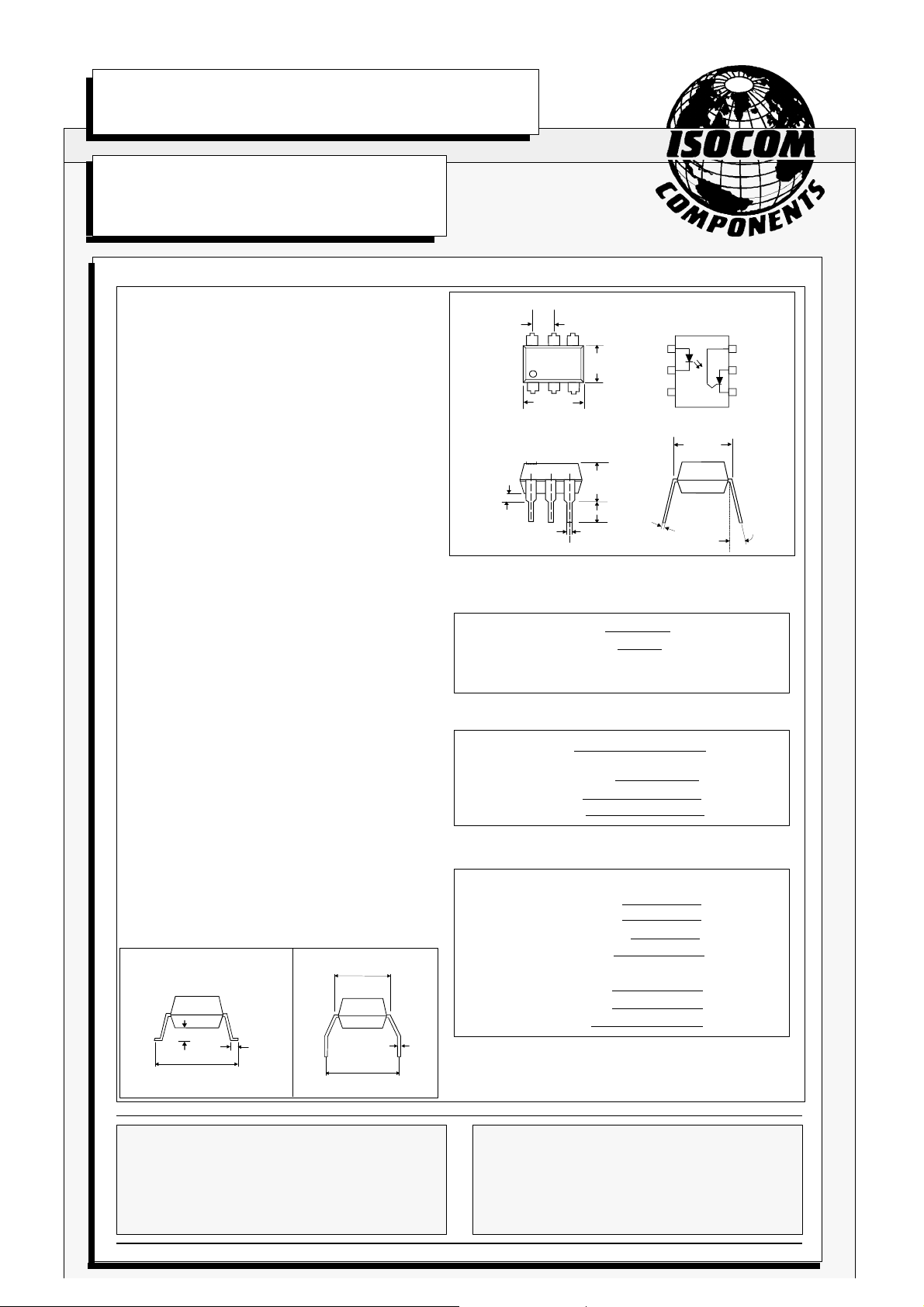
Dimensions in mm
1
2 5
3
8.3 max.
0.25
0.5
min.
2.54
7.0
6.0
7.62
max.
5.1
max.
3.9
3.1
0.48
ABSOLUTE MAXIMUM RATINGS
(25°C unless otherwise specified)
Storage Temperature -55°C to + 150°C
Operating Temperature -55°C to + 100°C
Lead Soldering Temperature
(1/16 inch (1.6mm) from case for 10 secs) 260°C
)
INPUT DIODE
Forward Current 60mA
Forward Current (Peak)
(1µs pulse, 300 pps) 3A
Reverse Voltage 6V
Power Dissipation 100mW
6
4
15°
Max
APPLICATIONS
l 10A, T
l 25W Logic Indicator Lamp Driver
l 400V Symmetrical transistor coupler
OPTION SM
SURFACE MOUNT
2
L compatible, Solid State Relay
OPTION G
1.2
0.6
10.2
9.5
1.4
0.9
8.3 max
10.16
ISOCOM COMPONENTS LTD
Unit 25B, Park View Road West,
Park View Industrial Estate, Brenda Road
Hartlepool, Cleveland, TS25 1YD
Tel: (01429) 863609 Fax :(01429) 863581
5/12/00
0.26
DETECTOR
Peak Forward Voltage
H11C1, H11C2, H11C3 200V*
H11C4, H11C5, H11C6 400V*
1
1
Peak Reverse Gate Voltage 6V
RMS On-state Current 300mA
Peak On-state Current
(100µs, 1% duty cycle) 10A
Surge Current (10ms) 5A
Power Dissipation 300mW
*1 IMPORTANT : A resistor must be connected
between gate and cathode (pins 4 & 6) to prevent false
firing (R
< 56kΩ)
GK
ISOCOM INC
1024 S. Greenville Ave, Suite 240,
Allen, TX 75002 USA
Tel: (214) 495-0755 Fax: (214) 495-0901
e-mail info@isocom.com
http://www.isocom.com
DB92010-AAS/A4
Page 2

ELECTRICAL CHARACTERISTICS ( TA= 25°C Unless otherwise noted )
PARAMETER MIN TYP MAX UNITS TEST CONDITION
Input Forward Voltage (VF) 1.2 1.5 V IF = 10mA
Reverse Voltage (VR) 3 V IR = 10µA
Output Peak Off-state Voltage (V
(note 2) H11C1, H11C2, H11C3 200 V RGK=10kΩ, ID= 50µA,
DM
)
TA= 100°C
H11C4, H11C5, H11C6 400 V RGK=10kΩ,ID=150µA,
TA=100°C
Peak Reverse Voltage (V
H11C1, H11C2, H11C3 200 V RGK=10kΩ, ID= 50µA,
RM
)
TA=100°C
H11C4, H11C5, H11C6 400 V RGK=10kΩ,ID=150µA,
TA=100°C
On-state Voltage (V
Off-state Current (I
H11C1, H11C2, H11C3 50 µA RGK=10kΩ, IF= 0,
) 1.1 1.3 V ITM = 300mA
TM
)
DM
VDM=200V, TA=100°C
H11C4, H11C5, H11C6 150 µA RGK=10kΩ, IF= 0,
VDM=400V, TA=100°C
Reverse Current (IR )
H11C1, H11C2, H11C3 50 µA RGK=10kΩ, IF= 0,
VDM=200V, TA=100°C
H11C4, H11C5, H11C6 150 µA RGK=10kΩ, IF= 0,
VDM=400V, TA=100°C
Coupled Input Current to Trigger ( I
) (note 2)
FT
H11C1, H11C2, H11C4, H11C5 20 mA VAK =50V, RGK=10kΩ
H11C3, H11C6 30 mA VAK =50V, RGK=10kΩ
H11C1, H11C2, H11C4, H11C5 11 mA VAK=100V, RGK=27kΩ
H11C3, H11C6 14 mA VAK=100V, RGK=27kΩ
Coupled dv/dt, Input to Output (dv/dt) 500 V/µs
Input to Output Isolation Voltage V
Input-output Isolation Resistance R
Input-output Capacitance Cf 2 pF V = 0, f =1MHz
5300 V
ISO
7500 V
11
10
ISO
RMS
PK
Ω V
See note 1
See note 1
= 500V (note 1)
IO
5/12/00
Note 1 Measured with input leads shorted together and output leads shorted together.
Note 2 Special Selections are available on request. Please consult the factory.
DB92010-AAS/A4
Page 3

µ
Input Current to Trigger vs.
Anode to Cathode Voltage
100
FT
40
20
RGK =300Ω
10
1kΩ
4
2
10kΩ
1.0
27kΩ
0.4
56kΩ
0.2
Normalized input current to trigger I
0.1
1 5 10 50 100 200
Anode to cathode voltage VAK ( V )
Normalized to
VAK = 50V
RGK =10kΩ
TA = 25 °C
Input Current to Trigger vs.
Ambient Temperature
12
FT
RGK =300Ω
10
1kΩ
4
2
10kΩ
1.0
27kΩ
0.4
56kΩ
0.2
Normalized input current to trigger I
0.1
Normalized to VAK = 50V,
RGK =10kΩ, TA = 25 °C
-60 -40 -20 0 20 40 60 80 100 120
Ambient temperature TA ( °C )
Input Current to Trigger Distribution
vs. Ambient Temperature
10
FT
Normalized to
VAK = 50V
4
RGK =10kΩ
TA = 25 °C
90th percentile
2
FT
100
40
20
10
4
1
10th percentile
0.4
2
1
Input Current to Trigger vs.
Pulse Width
RGK =300Ω
1kΩ
27kΩ
10kΩ
56kΩ
Normalized to
VAK = 50V
RGK =10kΩ
TA = 25 °C
0.4
0.2
Normalized input current to trigger I
0.1
-40 -20 0 20 40 60 80 100
Ambient temperature TA ( °C )
Turn on Time vs. Input Current
24
22
10kΩ
RGK=1kΩ
20
18
s)
(
16
on
VAK = 50V
ton = td + t
tr = 1µs
r
14
12
10
8
Turn on time t
56kΩ
6
4
2
0
0 10 20 30 40 50 60 70 80 90 100
Input current IF (mA)
5/12/00
0.2
Normalized input current to trigger I
0.1
1 2 4 6 10 20 40 60 100 200 400 1000
Pulse width ( µs )
Input Characteristics IF vs. V
100
40
20
10
(mA)
F
4
100°C
25°C
-55°C
2
1
0.4
Forward current I
0.2
0.1
0 0.5 1 1.5 2 2.5 3
Forward voltage VF ( V )
F
DB92010-AAS/A4
Page 4

µ
Holding Current vs. Ambient
µ
Temperature
10000
Normalized to
VAK = 50V
RGK =10kΩ
TA = 25 °C
A)
(
H
4000
2000
1000
RGK =300Ω
1kΩ
400
200
100
Holding current I
40
10kΩ
27kΩ
56kΩ
20
10
-60 -40 -20 0 20 40 60 80 100 120
Ambient temperature TA ( °C )
Maximum Transient Thermal Impedence
1000
1. Lead temperature measured at the
widest portion of the SCR anode lead.
400
2. Ambient temperature measured at
a point 1/2" from the device.
200
100
Junction to ambient
40
20
10
4
2
Transient thermal impedance ( °C / Watt )
1
0.001 0.01 0.1 1 2 4 10 100
Time (seconds)
Junction to lead
Off State Forward Current vs.
Ambient Temperature
10000
)
D
4000
2000
Normalized to
VAK = 50V
TA = 25 °C
1000
400
200
100
40
20
VAK = 400V
VAK = 50V
VAK = 200V
10
4
2
1
Normalized forward current off state ( I
0 25 50 75 100
Ambient temperature TA ( °C )
100
90
80
70
60
50
40
30
20
10
Maximum allowable temperature ( °C )
0
On State Current vs. Maximum
Allowable Temperature
1. Ambient temp. half-sine wave avg
2. Ambient temp. DC current
3. Anode lead temp. half-sine wave avg
4. Anode lead temp. DC current
1. 2. 4.3.
0 0.2 0.4 0.6 0.8 1.0
On state current ( Α )
s)
dV/dt vs. Ambient temperature
400
1000
RGK =300Ω
2
1
On State Characteristics
100
0.2
40
10
1kΩ
10kΩ
4
1
27kΩ
(A)
T
0.1
0.04
0.02
0.01
On state current I
0.4
56kΩ
0.1
25 50 75 100
Critical rate of rise applied forward voltage dV/dt (V/
5/12/00
Ambient temperature TA ( °C )
100°C
Junction temperature =
25°C
Junction temperature =
Increases to forward
breakover voltage
0 1 2 3 4
On state voltage VT ( V )
DB92010-AAS/A4
0.4
 Loading...