

ISOCM 6N137, ICPL2601 Datasheet
19/4/99
DB91063-AAS/A1
6N137
ICPL2601
HIGH CMR, VERY HIGH SPEED
OPTICALLY COUPLED ISOLATOR
LOGIC GATE OUTPUT
ABSOLUTE MAXIMUM RATINGS
(25°C unless otherwise specified)
Storage Temperature -55°C to + 125°C
Operating Temperature 0°C to + 70°C
Lead Soldering Temperature
(1/16 inch (1.6mm) from case for 10 secs) 260°C
INPUT DIODE
Average Forward Current 20mA
Reverse Voltage 5V
DETECTOR
Enable Input Voltage ( VE ) 5.5V
(not to exceed VCC by more than 500mV)
Reverse Supply Voltage(-VCC ) -500mV
Supply Voltage(VCC ) 7V
(1 minute maximum)
Output Current ( IO ) 25mA
Output Voltage ( VO ) 7V
Collector Output Power Dissipation 40mW
APPROVALS
l UL recognised, File No. E91231
DESCRIPTION
The 6N137 / ICPL2601 optocouplers consist of
a GaAsP light emitting diode and a high gain
integrated photo detector to provide 2500Volts
RMS
electrical isolation between input and output. An
enable input allows the detector to be strobed.
The output of the detector I.C. is an open
collector Schottky clamped transistor. The
ICPL2601 has an internal shield which provides
a guaranteed common mode transient immunity
specification of 1000V/µs minimum.This unique
design provides maximum ac and dc circuit
isolation while achieving TTL compatibility. The
coupled parameters are guaranteed over the
temperature range of 0°C to 70°C, such that a
maximum input signal of 5mA will provide a
minimum output sink current of 13mA(equivalent
to fan-out of eight gates)
FEATURES
l High speed - 10MBit/s
l High Common Mode Transient
Immunity 10kV/µs typical
l Logic gate output
l ICPL2601 has improved noise shield
for superior common mode rejection
l Options :-
10mm lead spread - add G after part no.
Surface mount - add SM after part no.
Tape&reel - add SMT&R after part no.
APPLICATIONS
l Line receiver, data transmission
l Computer-peripheral interface
l Data multiplexing
l Pulse transformer replacement
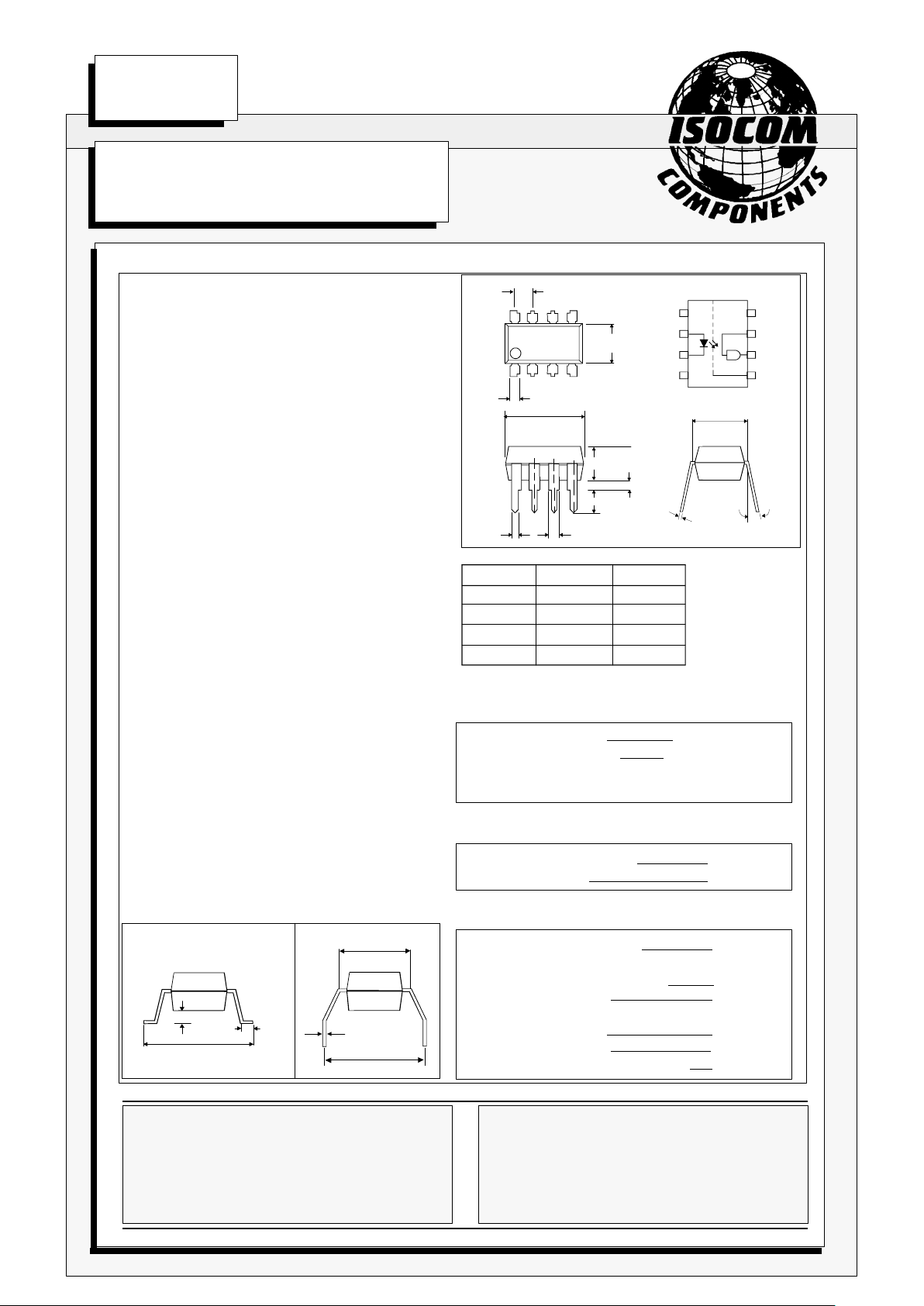
0.3
0.5
Dimensions in mm
6.9
6.3
1.3
15°
Max
3.3
4.0
3.6
2.54
9.7
9.1
0.5
1.3
* ICPL2601 NOISE SHIELD
7.62
4
3
2
1
8
7
6
5
*
OPTION GOPTION SM
10.16
10.2
9.5
0.3
1.2
0.6
1.4
0.9
7.62
SURFACE MOUNT
INPUT ENABLE OUTPUT
H H L
L H H
H L H
L L H
TRUTH TABLE
A 0.1µF bypass
capacitor must be
connected between
pins 8 and 5 ( See
note 1)
V
CC
GND
ISOCOM INC
1024 S. Greenville Ave, Suite 240,
Allen, TX 75002 USA
Tel: (214) 495-0755 Fax: (214) 495-0901
e-mail info@isocom.com
http://www.isocom.com
ISOCOM COMPONENTS LTD
Unit 25B, Park View Road West,
Park View Industrial Estate, Brenda Road
Hartlepool, TS25 1YD England Tel: (01429)863609
Fax : (01429) 863581 e-mail sales@isocom.co.uk
http://www.isocom.com
DB91063-AAS/A1
19/4/99
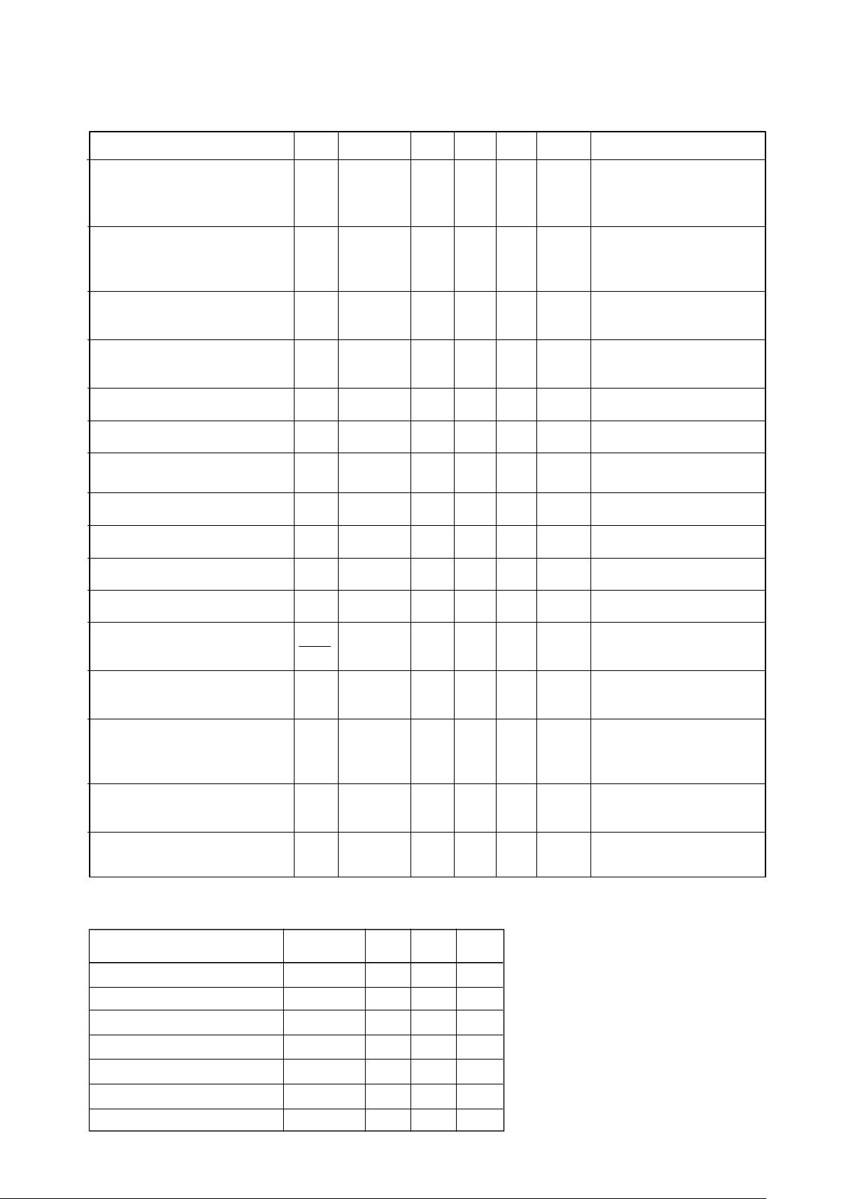
ELECTRICAL CHARACTERISTICS ( TA= 0°C to 70°C Unless otherwise noted )
PARAMETER SYM DEVICE MIN TYP* MAX UNITS TEST CONDITION
High Level Output Current I
OH
0.02 250 µA V
CC
= 5.5V, VO = 5.5V
IF = 250µA, VE = 2V
Low Level Output Voltage V
OL
0.4 0.6 V V
CC
= 5.5V, IF = 5mA
VE = 2V
IOL (sinking ) = 13mA
High Level Supply Current I
CCH
10 15 mA V
CC
= 5.5V, IF = 0mA
VE = 0.5V
Low Level Supply Current I
CCL
15 18 mA V
CC
= 5.5V, IF = 10mA
VE = 0.5V
High Level Enable Current I
EH
-1.0 mA V
CC
= 5.5V, VE = 2V
Low Level Enable Current I
EL
-1.5 -2.0 mA V
CC
= 5.5V, VE = 0.5V
High Level Enable Voltage V
EH
2 V V
CC
= 5.5V, IF = 10mA
(note 10)
Low Level Enable Voltage V
EL
0.8 V V
CC
= 5.5V, IF = 10mA
Input Forward Voltage V
F
1.55 1.75 V IF = 10mA, TA = 25oC
Input Reverse Breakdown Voltage V
BR
5 V IR = 10µA, TA = 25oC
Input Capacitance C
IN
60 pF VF = 0, f = 1MHz
Temperature Coefficient ∆V
F
-1.4 mV/°C IF = 10mA
of Forward Voltage ∆T
A
Input-output Isolation Voltage V
ISO
2500 5000 V
RMS
R.H.equal to or less than
(note 3) 50%, t = 1min, TA= 25°C
Input-output Insulation Leakage I
I-O
1 µA R.H. = 45%
Current (note 3) t = 5s, TA= 25°C
V
I-O
= 3000V dc
Resistance (Input to Output) R
I-O
10
12
Ω V
I-O
= 500V dc
(note 3)
Capacitance (Input to Output) C
I-O
0.6 pF f = 1MHz
(note 3)
* All typicals at TA= 25°C
RECOMMMENDED OPERATING CONDITIONS
PARAMETER SYMBOL MIN MAX UNITS
Input Current, Low Level I
FL
0 250 µA
Input Current, High Level I
FH
6.3* 15 mA
Supply Voltage, Output V
CC
4.5 5.5 V
Enable Voltage, Low Level V
EL
0 0.8 V
Enable Voltage, High Level V
EH
2.0 V
CC
V
Fan Out ( TTL Load ) N 8
Operating Temperature T
A
0 70 °C
*6.3mA is a guard banded
value which allows for at least
20% CTR degradation.
Initial input current threshold
value is 5.0mA or less
 Loading...