

ISOCM 4N37X, 4N37, 4N36X, 4N36, 4N35X Datasheet
...
24/11/00
4N35X, 4N36X, 4N37X,
4N35, 4N36, 4N37,
OPTICALLY COUPLED
ISOLATOR
PHOTOTRANSISTOR OUTPUT
APPROVALS
l UL recognised, File No. E91231
'X' SPECIFICATION APPROVALS
ll VDE 0884 in 3 available lead forms : -
- STD
- G form
- SMD approved to CECC 00802
l EN60950 approval pending
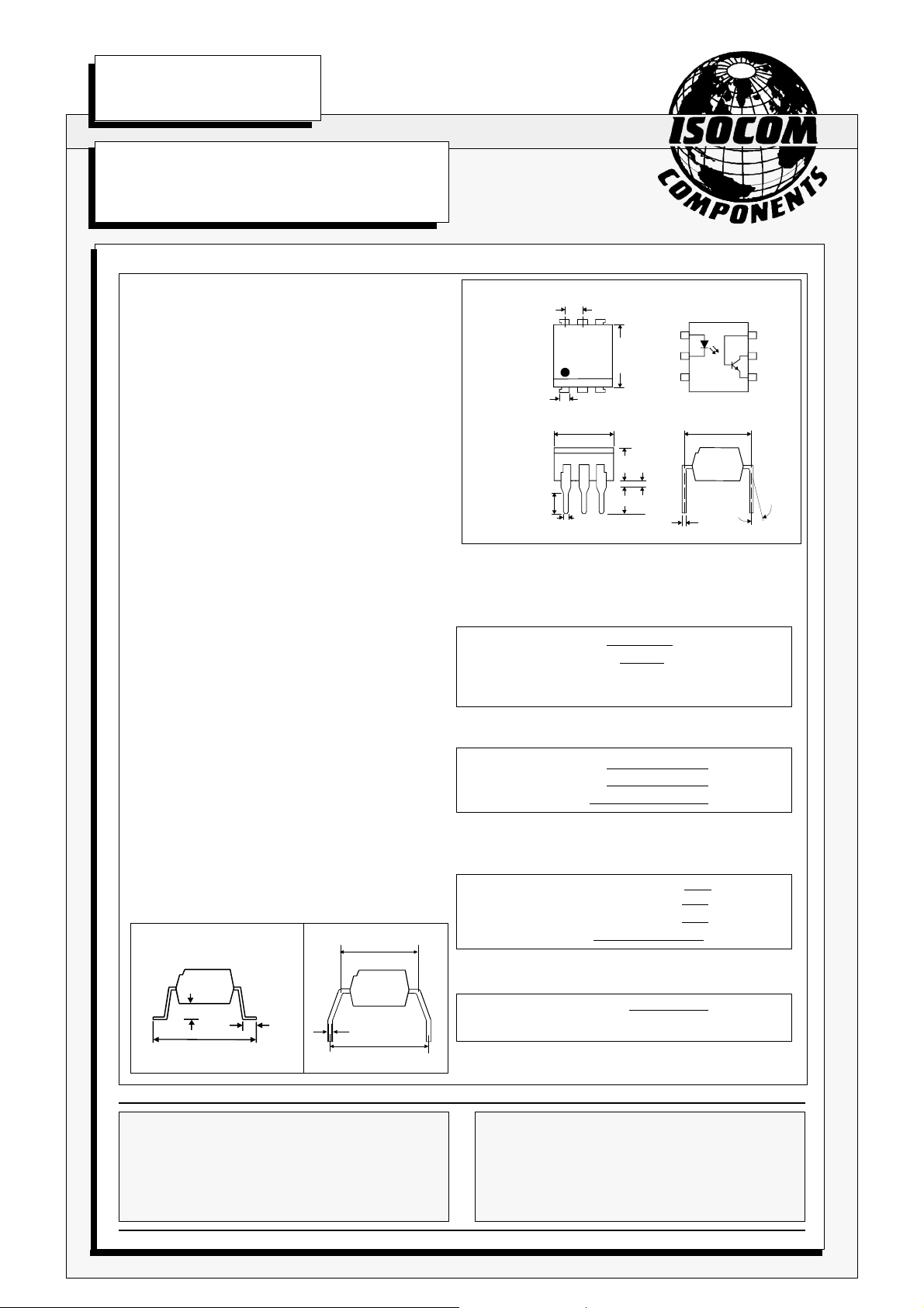
DESCRIPTION
The 4N35, 4N36, 4N37 series of optically
coupled isolators consist of infrared light
emitting diode and NPN silicon photo transistor
in a standard 6 pin dual in line plastic package.
FEATURES
l Options :-
10mm lead spread - add G after part no.
Surface mount - add SM after part no.
Tape&reel - add SMT&R after part no.
l High Current Transfer Ratio (100% min.)
l High Isolation Voltage (5.3kV
l All electrical parameters 100% tested
l Custom electrical selections available
RMS
,7.5kV
PK
APPLICATIONS
l DC motor controllers
l Industrial systems controllers
l Measuring instruments
l Signal transmission between systems of
different potentials and impedances
OPTION SM
SURFACE MOUNT
OPTION G
7.62
2.54
7.0
6.0
Dimensions in mm
1
2 5
3 4
1.2
7.62
6.62
4.0
3.0
0.5
3.0
0.5
3.35
ABSOLUTE MAXIMUM RATINGS
(25°C unless otherwise specified)
Storage Temperature -55°C to + 150°C
Operating Temperature -55°C to + 100°C
Lead Soldering Temperature
(1/16 inch (1.6mm) from case for 10 secs) 260°C
)
INPUT DIODE
Forward Current 60mA
Reverse Voltage 6V
Power Dissipation 105mW
OUTPUT TRANSISTOR
Collector-emitter Voltage BV
Collector-base Voltage BV
Emitter-collector Voltage BV
Power Dissipation 160mW
CEO
CBO
ECO
POWER DISSIPATION
6
7.62
13°
Max
0.26
30V
70V
6V
0.6
0.1
10.46
9.86
1.25
0.75
0.26
10.16
ISOCOM COMPONENTS LTD
Unit 25B, Park View Road West,
Park View Industrial Estate, Brenda Road
Hartlepool, Cleveland, TS25 1YD
Tel: (01429) 863609 Fax :(01429) 863581
Total Power Dissipation 200mW
(derate linearly 2.67mW/°C above 25°C)
ISOCOM INC
1024 S. Greenville Ave, Suite 240,
Allen, TX 75002 USA
Tel: (214) 495-0755 Fax: (214) 495-0901
e-mail info@isocom.com
http://www.isocom.com
DB90046M-AAS/A1
24/11/00
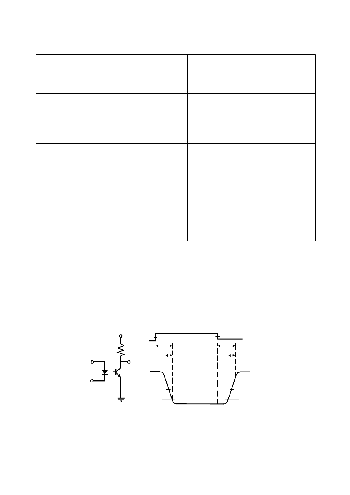
ELECTRICAL CHARACTERISTICS ( TA= 25°C Unless otherwise noted )
PARAMETER MIN TYP MAX UNITS TEST CONDITION
Input Forward Voltage (VF) 1.2 1.5 V IF = 10mA
Reverse Voltage (VR) 6 V IR = 10µA
Reverse Current (IR) 10 µA VR = 6V
Output Collector-emitter Breakdown (BV
( Note 2 )
Collector-base Breakdown (BV
Emitter-collector Breakdown (BV
Collector-emitter Dark Current (I
Collector-base Dark Current (I
) 30 V IC = 1mA
CEO
) 70 V IC = 100µA
CBO
) 6 V IE = 100µA
ECO
) 50 nA VCE = 10V
CEO
) 20 nA VCE = 10V
CBO
Coupled Current Transfer Ratio (CTR) 100 % 10mA IF , 10V V
Collector-emitter Saturation VoltageV
Input to Output Isolation Voltage V
Input-output Isolation Resistance R
CE(SAT)
5300 V
ISO
7500 V
10
5x10
ISO
0.3 V 10mA I
RMS
PK
Ω V
See note 1
See note 1
= 500V (note 1)
IO
, 0.5mA I
F
Turn-on Time ton 5 10 µs VCC = 10V ,
Turn-off Time toff 5 10 µs IC= 2mA, RL = 100Ω
Output Rise Time tr 3.5 µs ( FIG 1)
Output Fall Time tf 4.9 µs
Note 1 Measured with input leads shorted together and output leads shorted together.
Note 2 Special Selections are available on request. Please consult the factory.
CE
C
RL = 100Ω
V
CC
Input
Output
Output
10%
90%
t
on
t
r
FIG 1
t
off
t
f
10%
90%
DB90046M-AAS/A1
 Loading...