

iSMA iSMA-B-4I4O-H, iSMA-B-8I, iSMA-B-8U-IP, iSMA-B-4I4O-H-IP, iSMA-B-8I-IP User Manual
...Page 1
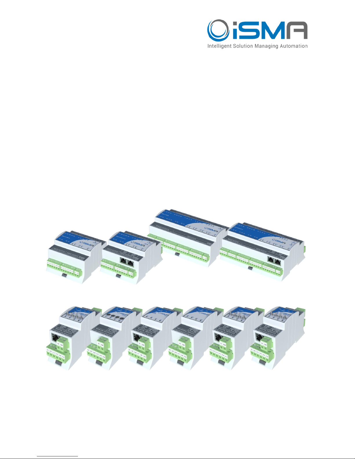
MINI and MIX Series
I/O modules
User Manual
Modbus
Global Control 5 Sp. z o.o.
Warsaw, Poland
www.gc5.pl
Page 2

Table of contents
1 Introduction ................................................................................................................................................ 5
1.1 Revision history .................................................................................................................................................... 5
1.2 Safety rules............................................................................................................................................................ 6
1.3 .Technical specifications .................................................................................................................................... 7
1.4 Summary table for all modules ......................................................................................................................... 9
1.5 Dimension ........................................................................................................................................................... 11
1.6 Power supply connection ................................................................................................................................ 12
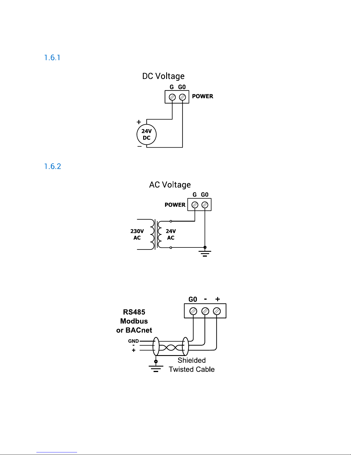
DC power connection.....................................................................................................................................................12
AC power connection .....................................................................................................................................................12
1.7 Connecting the communication bus (RS485) ............................................................................................. 12
1.8 LED Indicators ................................................................................................................................................... 13
1.9 Grounding and shielding .................................................................................................................................. 14
1.10 RS485 network termination ............................................................................................................................ 14
1.11 Setting Module Address on Modbus Network ............................................................................................ 15
1.12 Baud rate selection ........................................................................................................................................... 15
1.13 Protocol selection ............................................................................................................................................. 16
1.14 Restoring the default settings ........................................................................................................................ 16
1.15 Default Settings ................................................................................................................................................. 17
2 Configuration registers ........................................................................................................................... 18
2.1 Firmware version and module type (30001) ............................................................................................... 18
2.2 Module address (30002) ................................................................................................................................. 18
2.3 Baud rate and protocol (30003) ..................................................................................................................... 19
2.4 Counter of received messages (30004) ....................................................................................................... 19
2.5 Counter of error messages (30006) .............................................................................................................. 19
2.6 Counter of sent messages (30008) .............................................................................................................. 19
2.7 Up time (30012) ................................................................................................................................................ 19
2.8 Hardware_version (30130) .............................................................................................................................. 20
2.9 MAC_address (30131) ..................................................................................................................................... 20
2.10 Device actions (40001) .................................................................................................................................... 20
2.11 Baud rate (40136) ............................................................................................................................................. 20
2.12 Stop bits (40137)............................................................................................................................................... 20
2.13 Data bits (40138) .............................................................................................................................................. 21
2.14 Parity bit (40139) ............................................................................................................................................... 21
2.15 Response delay time (40140) ......................................................................................................................... 21
2.16 Watchdog time (40141) ................................................................................................................................... 21
3 Local I/O ................................................................................................................................................... 23
3.1 Universal Inputs connections ......................................................................................................................... 23
Connection of Universal Input to measure voltage 0 – 10V ..................................................................................23
Connection of Universal Input to measure current 0 – 20 mA .............................................................................23
Connection of Universal Input to measure temperature ........................................................................................24
Connection of Universal Input as a Digital Input (Dry Contact) .............................................................................24
3.2 Universal Inputs MODBUS Registers ............................................................................................................ 25
Status of Universal Inputs working as Digital Inputs (30017) ...............................................................................25
Universal Input measure voltage (current) 1 - 8 (30071, 30073, 30075, 30077, 30079, 30087, 30089, 30091)
25
Universal Input measure temperature 1 - 8 (30072, 30074, 30076, 30078, 30080, 30095, 30097, 30099) 25
Universal Input measure resistance 1 - 8 (30103, 30104 – 30117, 30118) .......................................................25
Universal Input configuration 1 - 8 (40151 – 40158) ..............................................................................................25
Filter time constant of the Universal Input 1 - 8 (40159 – 40166) .......................................................................26
Resolution of the universal inputs (40167) ...............................................................................................................26
3.3 Digital Inputs Connections .............................................................................................................................. 27
Connection of Digital Input (Dry Contact) ..................................................................................................................27
Page 3

MINI and MIX Series I/O modules/Modbus
version 1.3 www.gc5.pl Page 3 / 73
3.4 Digital Inputs MODBUS Registers .................................................................................................................. 27
State of Digital Inputs (30016) .....................................................................................................................................27
Counter 1 – 12 (40023, 40024 – 40045, 40046) .....................................................................................................27
Resetting counters (40022)..........................................................................................................................................28
3.5 Analog Outputs Connections .......................................................................................................................... 28
Connection of Analog Output 0 – 10 V ......................................................................................................................28
Connecting relay to Analog Output .............................................................................................................................28
Connection an actuator to Analog Output .................................................................................................................29
3.6 Analog Outputs MODBUS Registers ............................................................................................................. 29
State of Analog Outputs working as Digital Outputs (40019) ...............................................................................29
Value of the analog outputs 1 – 6 (40121 – 40126) ..............................................................................................29
Default state of the analog outputs (digital) (40144) ..............................................................................................29
Default state of the Analog Output 1 – 6 (40145 – 40150) .................................................................................. 30
Configuration mode of Analog Output 1 – 6 (40168 – 40173) ............................................................................ 30
Hand control status of analog outputs (30015) ...................................................................................................... 30
Hand control value of Analog Outputs 1 – 4 (30125 - 20128)...............................................................................31
3.7 Digital Outputs (relays) Connections ............................................................................................................ 32
Connecting the solenoid valve to the Digital Output ...............................................................................................32
Connecting a resistive load to the Digital Output .....................................................................................................32
Connecting a inductive load to the Digital Output ...................................................................................................32
3.8 Digital Outputs (relays) MODBUS Registers ................................................................................................ 33
State of Digital Outputs (40018) ..................................................................................................................................33
Default state of Digital Outputs (40143) ....................................................................................................................33
Hand control status of Digital Outputs (30015) .......................................................................................................33
3.9 Triac Outputs Connections ............................................................................................................................. 34
Connecting the solenoid valve to the Triac Output ..................................................................................................34
Connecting a resistive load to the Triac Output .......................................................................................................34
3.10 Triac Outputs MODBUS Registers ................................................................................................................. 35
State of Triac Outputs (40018) ....................................................................................................................................35
Default state of triac outputs (40143) ........................................................................................................................35
Value of the Triac PWM outputs 1 – 4 (40121 – 40124) ......................................................................................35
Default state of the Triac PWM outputs 1 – 4 (40145 – 40148) ..........................................................................35
Configuration mode of Triac Output 1 – 4 (40168 – 40171).................................................................................35
Hand control status of Triac Outputs (30015) ..........................................................................................................36
3.11 Special application modes for 4I4O-H, 4I4O-H-IP, 4U4O-H and 4U4O-H-IP ........................................... 37
Operation Mode registers (40176,40180,40184,40188) .........................................................................................38
Time Value registers (40177,40181,40185,40189) ..................................................................................................41
Command register (40020) ..........................................................................................................................................42
Block Inputs register (40021) .......................................................................................................................................42
Setpoint registers (40178,40182,40186,40190) .......................................................................................................42
Differential registers (40179,40183,40187,40191) ..................................................................................................42
4 WEB Configuration- only IP version ...................................................................................................... 43
4.1 Web server access ............................................................................................................................................ 43
4.2 Device page ........................................................................................................................................................ 43
4.3 Local I/O status and configuration ................................................................................................................ 44
Universal Inputs ..............................................................................................................................................................44
Special application modes configuration ..................................................................................................................45
Digital Inputs ....................................................................................................................................................................46
Digital Outputs.................................................................................................................................................................46
Analog Outputs ...............................................................................................................................................................47
4.4 RS485 Configuration ........................................................................................................................................ 48
4.5 IP Configuration................................................................................................................................................. 49
4.6 Device management ........................................................................................................................................ 50
4.7 Contact ................................................................................................................................................................ 50
5 Modbus TCP/IP modules ....................................................................................................................... 51
5.1 Modbus TCP/IP ................................................................................................................................................. 51
Page 4

MINI and MIX Series I/O modules/Modbus
version 1.3 www.gc5.pl Page 4 / 73
5.2 Module as Modbus TCP/IP Gateway to RS485 .......................................................................................... 51
6 List of all Modbus Registers .................................................................................................................. 53
7 List of supported temperature sensors ................................................................................................ 62
Page 5

MINI and MIX Series I/O modules/Modbus
version 1.3 www.gc5.pl Page 5 / 73
1 Introduction
1.1 Revision history
Rev
Date
Description
1.0 2015.08.28
First edition
1.1 2016.02.01
The reason for the creation of new version of the document:
• At 12.2015 GC5 released a new hardware version for MIX module with more
powerful processor and USB port. For this hardware and for all MINI series
devices we released firmware 4.0 which contains bug fix, firmware
improvement and also rebuilt BACnet protocol (new object, COV).
• All modules purchased as of 2016 have improved versions of the relays, which
allow to increase the capacitive load. Details of the technical specifications.
• Note: This document was created for devices with firmware version 4.0 and
above. For previous firmware version please read Modbus Manual version 1.0.
• Changes in Document:
• Added to the technical specifications information about the capacitive load
relay.
• Added to the technical specifications information about load Triac Outputs.
• Added description of the new MINI module 4x Triac Outputs: 4TO-H and 4TO-H-
IP.
• MINI - 4I40-H and 4I40-H-IP Module built in application: Change of logic in the
Time relay mode. Now, timer counts from falling edge (before from rising
edge).
• New gateway functionality blocking Send Modbus Error.
• Changed tables with PT1000 and NI1000 for more accurate, because new FW
measure resistance for this sensors with accuracy 0,1 Ω.
1.2
2017.01.03
The reason for the creation of new version of the document:
New functions:
• New HVAC functions Heating and Cooling in 4U4O based on output
thermostatic control with a setpoint and differential value setting;
• Added new input mode for 4I4O: Time Relay NC [ms], Time Relay NO and NC in
seconds, Input Forwarding;
• Added new input mode for 4U4O: Ordinary IO, Monostable Relay, Bistable Relay,
Time Relay NO and NC [ms], Time Relay NO and NC in seconds, Input
Forwarding, Heating, Cooling with corresponding BACnet objects and Modbus
registers;
• Added reset output to default after input mode change in 4U4O and 4I4O;
Improvements:
• Improved BACnet COV Increment can now have values with resolution 0.1;
• Added BACnet COV Increment access (read/write) through USB;
• Added power Led flashing after IO watchdog triggered;
• Changed IO watchdog reset after read/write registers through USB;
• Added immediately detecting sensors short circuit and disconnection
regardless of filter settings on universal inputs;
Fixed bugs:
• Fixed bug with Stop bits, was always 1;
1.3
2017.05.16
The reason for the creation of new version of the document:
Page 6

MINI and MIX Series I/O modules/Modbus
version 1.3 www.gc5.pl Page 6 / 73
New functions:
• added Hardware Version information on main tab in web page and Modbus
register
• new action in the Modbus register no 0 – enter bootloader
• added RS485 biasing control for MINI modules with a hardware version >= 2.0
(option unavailable in MIX modules)
• www page: RS485 Biasing Resistors activation option (shows only in MINI
modules with a hardware >= 2.0)
Improvements:
• fixed modules names on web page (added -H for all modules with hand
operation switches)
Table 1 Revision history
1.2 Safety rules
• Note: Incorrect wiring of this product can damage it and lead to other hazards.
Make sure the product has been correctly wired before turning the power ON.
• Before wiring, or removing/mounting the product, be sure to turn the power OFF.
Failure to do so might cause an electric shock.
• Do not touch electrically charged parts such as the power terminals. Doing so might
cause an electric shock.
• Do not disassemble the product. Doing so might cause an electric shock or faulty
operation.
• Use the product within the operating ranges recommended in the specification
(temperature, humidity, voltage, shock, mounting direction, atmosphere etc.).
Failure to do so might cause a fire or faulty operation
• Firmly tighten the wires to the terminal. Insufficient tightening of the wires to the
terminal might cause a fire.
Page 7

MINI and MIX Series I/O modules/Modbus
version 1.3 www.gc5.pl Page 7 / 73
1.3 Technical specifications
Power supply
Voltage
24 V AC/DC ± 20%
Power consumption
Module type
@ 24 VDC
@ 24 VAC
8I
0.4 W
0.6 VA
8I-IP
1.4 W
2.1 VA
8U
0.5 W
0.8 VA
8U-IP
1.5 W
2.3 VA
4I4O-H
1.2 W
1.8 VA
4I4O-H-IP
2.2 W
3.3 VA
4U4O-H
1.2 W
1.8 VA
4U4O-H-IP
2.2 W
3.3 VA
4U4A-H
2.2 W
3.3 VA
4U4A-H-IP
3.2 W
4.8 VA
4O-H
1.6 W
2.4 VA
4O-H-IP
2.6 W
3.9 VA
4TO-H
1.0 W
1.5 VA
4TO-H-IP
2.0 W
3.0 VA
MIX18
3.0 W
4.5 VA
MIX18-IP
4.4 W
6.6 VA
MIX38
5.0 W
7.5 VA
MIX38-IP
7.4 W
11.1 VA
Universal Inputs
Temperature input
• Measurement with attached RTDs
• accuracy ±0,1˚C
• For sensor Pt1000 and Ni1000 use 16-bit
resolution
Voltage input
• Voltage measurement from 0 - 10 V
• Input impedance 100 kΩ
• Measurement accuracy ±0,1%
• Measurement resolution 3 mV@12-bit and 1
mV@ 16-bit
Current input
• Current measurement 0 - 20 mA
• Required external resistor 200 Ω
• Measurement accuracy ±1,1%
• Measurement resolution 15 µA @ 12-bit and 5 µA
@ 16-bit
Resistive input
• Measurement of resistance from 0 to 1000 kΩ
• Measurement resolution for 20 kΩ load 20 Ω@12-
bit and 1 Ω@16-bit
• Measurement resolution for PT1000 and NI1000
0,1Ω@16bit
Page 8

MINI and MIX Series I/O modules/Modbus
version 1.3 www.gc5.pl Page 8 / 73
Resistance measurement method
The voltage divider
Dry contact input
Output current ~1 mA
Measurement resolution
12-bits (default) or 16-bits
Processing time
• 10 ms/channel at 12-bits
• 140 ms/channel at 16-bits
Digital Inputs
Type
Dry contact
Max input frequency
100 Hz
Analog Outputs
Voltage range
0 to 10 V
Max. load current
20 mA
Resolution
12-bits
Accuracy
±0.5%
Digital Outputs
(relays)
Contact material
AgSnO2
Resistive load AC1
3 A @ 230 VAC or 3 A @ 30 VDC
Inductive load AC3
75 VA @ 230 VAC or 30 W @ 30 VDC
Capacitive load
• 50 W @ LED + PS 230 VAC
• 100 W @ fluorescent lamps with electronic
ballast
• 75 W @ CFL Compact fluorescent lamp
Digital Outputs
(relays)
4O-H and 4O-H-IP
Contact material
AgSnO2
Resistive load AC1
8 A @ 230 VAC or 8 A @ 30 VDC
Inductive load AC3
360 VA@ 230 VAC or 90 W @ 30 VDC
Capacitive load
• 120 W @ LED + PS 230 VAC
• 240 W @ fluorescent lamps with electronic
ballast
• 180 W @ CFL Compact fluorescent lamp
Triac Outputs
Continuous load per channel
0,5 A @ 20 VAC up to max. 250 VAC
Peak load per channel
1,5 A @ 20 VAC up to max. 250 VAC (30 s)
Gate Control
Zero crossing turn ON
Frequency Range
47 to 63 Hz
Snubber
Snubberless Triac
RS485 Interface
RS485
Up to 128 devices
Communication protocols
Modbus RTU, Modbus ASCII
or BACnet set by switch
Baud rate
From 2400 to 115200 set by switch
Address
0 to 99 set by switch
Ethernet
MIX18-IP, MIX38-IP
2x Fast Ethernet
Switch mode
Baud rate
10/100 Mb/s
8I-IP, 8U-IP, 4I4O-H-IP, 4U4O-H-IP, 4U4A-H-IP, 4O-H-IP, TO-H-IP
Page 9

MINI and MIX Series I/O modules/Modbus
version 1.3 www.gc5.pl Page 9 / 73
1x Fast Ethernet
IP Interface
Baud rate
10/100 Mb/s
USB
USB
Mini USB 2.0
Ingress protection
IP
IP40
Temperature
Storage
-40˚C to +85˚C
Operating
-10˚C to +50˚C
Humidity
Relative
5% to 95%
Connectors
Type
Removable
Maximum cable size
2.5 mm2
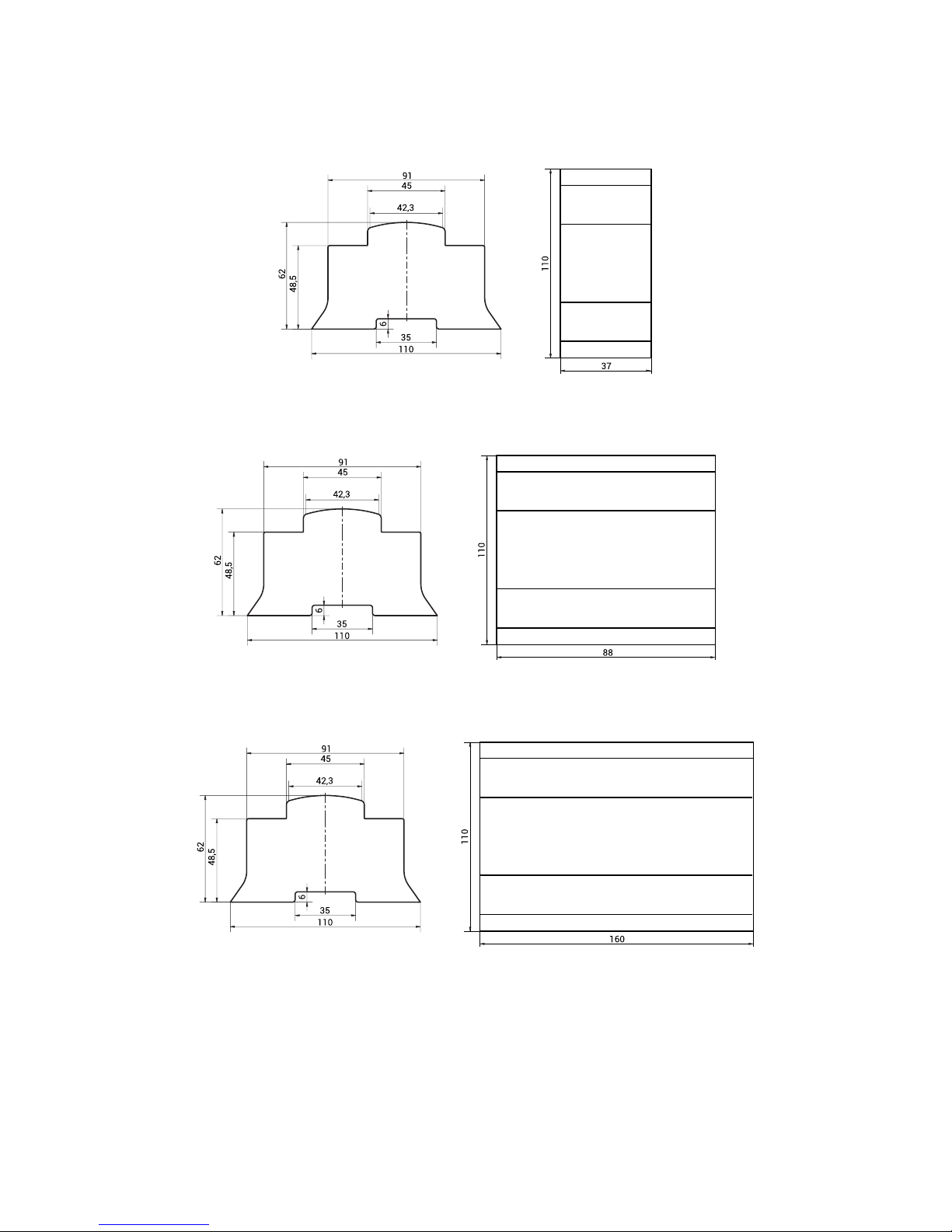
Dimension
MIX18, MIX18-IP
Width
110 mm
Length
88 mm
Height
62 mm
MIX38, MIX38-IP
Width
110 mm
Length
160 mm
Height
62 mm
MINI Series
Width
110 mm
Length
37 mm
Height
62 mm
Table 2 Technical specification
1.4 Summary table for all modules
Module
type
UI
DI
AO
DO
TO
Modbu
s
RS485
Modbus
TCP/IP
BACnet
MSTP
BA
Cn
et
IP
4I4O-H
4 4
✓ ✓
4I4O-H-IP
4 4
✓
✓ ✓
4O-H
4 (NC/NO-8A)
✓ ✓
4O-H-IP
4 (NC/NO-8A)
✓
✓ ✓
4U4A-H
4 4
✓ ✓
4U4A-H-IP
4 4
✓
✓ ✓
4U4O-H
4 4
✓ ✓
4U4O-H-IP
4 4
✓
✓ ✓
8I
8
✓ ✓
8I-IP
8
✓
✓ ✓
8U
8
✓ ✓
8U-IP
8
✓
✓ ✓
Page 10

MINI and MIX Series I/O modules/Modbus
version 1.3 www.gc5.pl Page 10 / 73
4TO-H
4
✓
✓ ✓
4TO-H-IP
4
✓
✓ ✓
MIX18
5 5 4 4
✓ ✓
MIX18-IP
5 5 4 4
✓
✓ ✓
MIX38
8
12 6 12
✓ ✓
MIX38-IP
8
12 6 12
✓
✓ ✓
RTU
ASCII
Modbus
Gateway
IP/RS485
Master
Slave
Table 3 Summary table for all modules
Page 11
MINI and MIX Series I/O modules/Modbus
version 1.3 www.gc5.pl Page 11 / 73
1.5 Dimension
Figure 1 MINI series dimension
Figure 2 MIX18 and MIX18-IP dimension
Figure 3 MIX38 and MIX38-IP dimension
Page 12
MINI and MIX Series I/O modules/Modbus
version 1.3 www.gc5.pl Page 12 / 73
1.6 Power supply connection
DC power connection
Figure 4 DC power supply connection
AC power connection
Figure 5 AC power supply connection
1.7 Connecting the communication bus (RS485)
Figure 6 RS485 connection
Page 13
MINI and MIX Series I/O modules/Modbus
version 1.3 www.gc5.pl Page 13 / 73
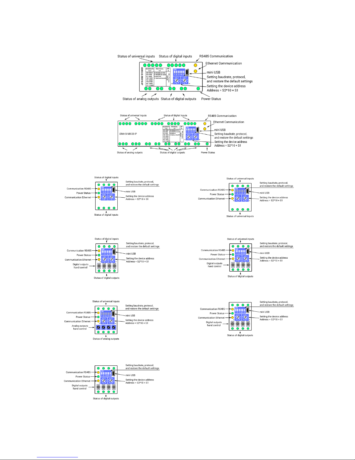
1.8 LED Indicators
Figure 7 Top panel MIX18-IP
Figure 8 Top panel MIX38-IP
Figure 9 Top panel 8I and 8I-IP
Figure 10 Top panel 8U and 8U-IP
Figure 11 Top panel 4I4O-H and 4I4O-H-IP
Figure 12 Top panel 4U4O-H and 4U4O-H-IP
Figure 13 Top panel 4U4A-H and 4U4A-H-IP
Figure 14 Top panel 4O-H and 4O-H-IP
Figure 15 Top panel 4TO-H and 4TO-H-IP
Page 14

MINI and MIX Series I/O modules/Modbus
version 1.3 www.gc5.pl Page 14 / 73
• The power LED is ON (green) when the module runs properly.
• Communication LED is ON (orange) for 20 ms after sending each message.
If the module receives/sends a lot of messages LED can be lit continuously.
• LEDs indicate the status of the Universal Inputs are lit when resistance connected to
the input is less than 5 kΩ (Dry Contact input is active).
WARNING! The LED also lights up when voltage connected to the input has a very low
potential.
• LEDs indicate the status of the digital inputs are lit when the input is active.
• LEDs indicate the status of the analog outputs are lit when output voltage or PWM
factor is different from 0.
• LEDs indicate the status of the digital outputs are lit when output is enabled.
1.9 Grounding and shielding
In most cases, IO modules will be installed in an enclosure along with other devices which
generate electromagnetic radiation. Relays, contactors, transformers, motor invertors etc.
are the examples of these devices. This electromagnetic radiation can induce electrical
noise into both power and signal lines, as well as direct radiation into the module causing
negative effects on the system. Appropriate grounding, shielding and other protective steps
should be taken at the installation stage to prevent these effects. These protective steps
include control cabinet grounding, cable shield grounding, protective elements for
electromagnetic switching devices, correct wiring as well as consideration of cable types
and their cross sections.
1.10 RS485 network termination
Transmission line effects often present a problem on data communication networks. These
problems include reflections and signal attenuation.
To eliminate the presence of reflections from the end of the cable, the cable must be
terminated at both ends with a resistor across the line equal to its characteristic
impedance. The both ends must be terminated since the direction of propagation is
bidirectional. In the case of an RS485 twisted pair cable this termination is typically 120 Ω.
Page 15
MINI and MIX Series I/O modules/Modbus
version 1.3 www.gc5.pl Page 15 / 73
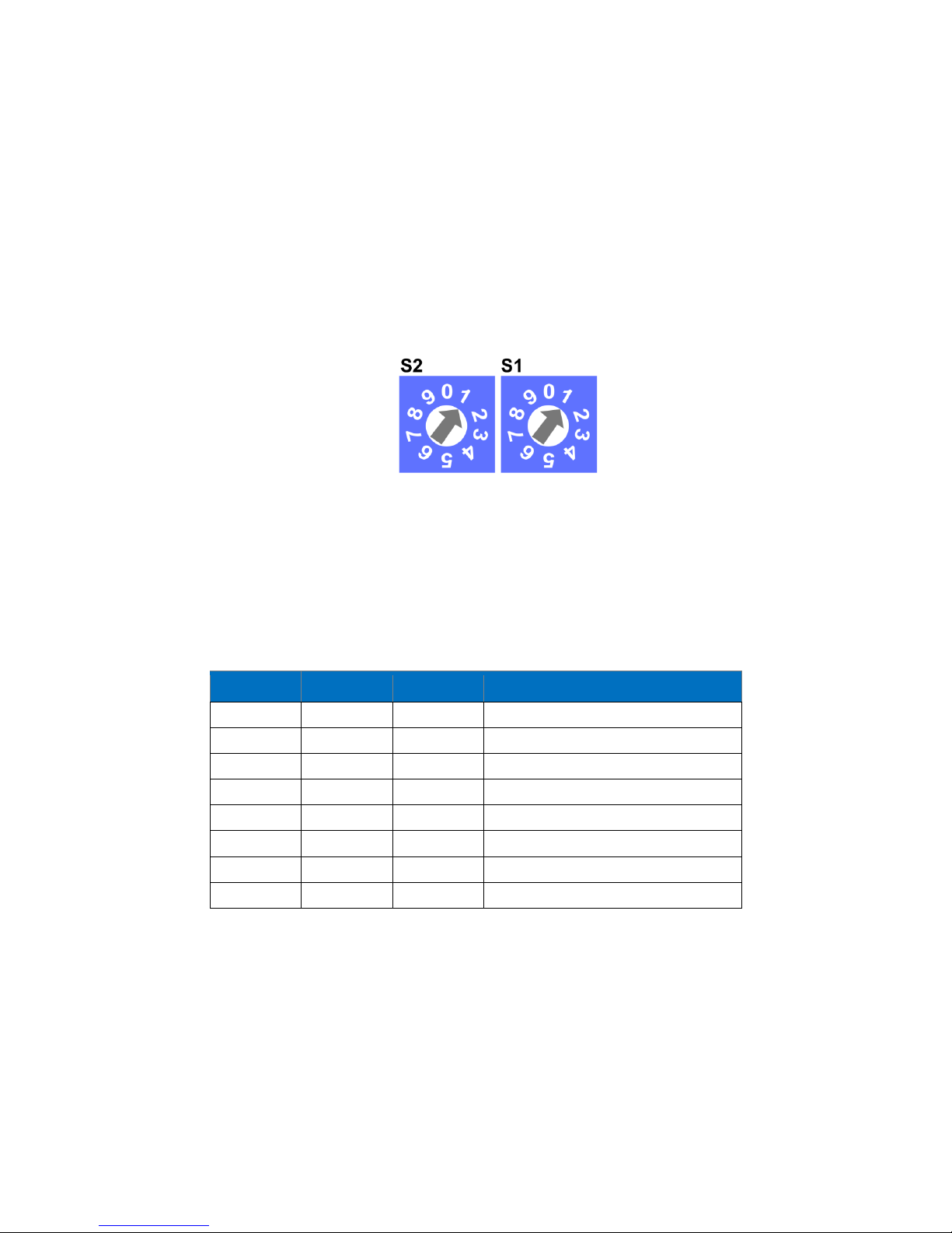
1.11 Setting Module Address on Modbus Network
To determine the address on the Modbus network, module provides two rotary switches S1
and S2 located on the top panel of the device.
It is possible to set the device address from 0 to 99.
The formula for setting the address:
Address = S2 • 10 + S1
Where S1 and S2 are values of switches.
The example:
Figure 16 Sample of setting address
Switches set as in figure above will set the module address to 11.
1.12 Baud rate selection
Transmission baud rate is determined by S3 switch (sections 1, 2 and 3) in accordance with
the following table:
1 2 3
Baud rate
OFF (0)
OFF (0)
OFF (0)
Defined by the user in the registry
OFF (0)
OFF (0)
ON (1)
76800
OFF (0)
ON (1)
OFF (0)
4800
OFF (0)
ON (1)
ON (1)
9600
ON (1)
OFF (0)
OFF (0)
19200
ON (1)
OFF (0)
ON (1)
38400
ON (1)
ON (1)
OFF (0)
57600
ON (1)
ON (1)
ON (1)
115200 (factory set)
Table 4 Baud rate selection
Page 16

MINI and MIX Series I/O modules/Modbus
version 1.3 www.gc5.pl Page 16 / 73
1.13 Protocol selection
Protocol selection is done by sections 4 and 5 of the S3 switch according to table below:
4 5 Protocol
OFF (0)
OFF (0)
Modbus RTU
OFF (0)
ON (1)
Modbus ASCII
ON (1)
OFF (0)
BACnet Master
ON (1)
ON (1)
BACnet Slave
Table 5 Protocol selection
1.14 Restoring the default settings
To restore the default configuration of all registers, follow the steps below:
1. Turn off power supply
2. Set section 6 of S3 switch to ON
3. Turn on power supply, power LED blinking
4. Switch section 6 of S3 switch to OFF to restore the default settings. To cancel the
reset, turn off the power and switch section 6 of S3 switch to the OFF position.
Page 17

MINI and MIX Series I/O modules/Modbus
version 1.3 www.gc5.pl Page 17 / 73
1.15 Default Settings
Out of the box device as well as after restoring default values procedure, has got the
following default registers values:
Register Name
Default Value
COUNTER
0
BAUD RATE
76800 (76800 bps)
STOP BITS
1
DATA BITS
8
PARITY BITS
0
RESPONSE DELAY
0
WATCHDOG TIME
0 ( disabled)
STATE OF THE DIGITAL OUTPUTS AFTER START
0
STATE OF THE ANALOG OUTPUTS (DIGITAL)
AFTER START
0
STATE OF THE ANALOG OUTPUTS AFTER START
0
UNIVERSAL INPUT CONFIGURATION
1
INPUT FILTER TIME CONSTANT
2
UNIVERSAL INPUT RESOLUTION
0
ANALOG OUTPUT CONFIGURATION
0
Only for modules with IP
USERNAME
platform
PASSWORD
1000
IP ADDRESS
192.168.1.123
MASK
255.255.255.0
GATEWAY
192.168.1.1
HTTP PORT
80
MODBUS TCP PORT
502
MODBUS TCP TIMEOUT
60s
RS485 TIMEOUT
1000ms
SEND MODBUS ERRORS
DISABLE
BACNET ID
826001
BACNET UDP PORT
47808 (0xBAC0)
Table 6 Default values
Page 18

MINI and MIX Series I/O modules/Modbus
version 1.3 www.gc5.pl Page 18 / 73
2 Configuration registers
WARNING! Changing the parameters concerning the transmission configuration (except to
registers which value is read from the switch) will only take effect after restarting the unit.
2.1 Firmware version and module type (30001)
In this register are encoded type and firmware version of module.
Low byte contains information about the type of module in accordance with table below:
Value
Type
8110 (0x5116)
8I
9110 (0x5B16)
8I-IP
8410 (0x5416)
8U
9410 (0x5E16)
8U-IP
8310 (0x5316)
4I4O-H
9310 (0x5D16)
4I4O-H-IP
8510 (0x5516)
4U4O-H
9510 (0x5F16)
4U4O-H-IP
8610 (0x5616)
4U4A-H
9610 (0x6016)
4U4A-H-IP
8210 (0x5216)
4O-H
9210 (0x5C16)
4O-H-IP
8710 (0x5716)
4TO-H
9710 (0x6116)
4TO-H-IP
5010 (0x3216)
MIX18
5110 (0x3316)
MIX38
5210 (0x3416)
MIX18-IP
5310 (0x3516)
MIX38-IP
Table 7 Firmware version and module type
High byte contains the module firmware version multiplied by 10.
The example:
In register 30001 is number 1281010 = 0x320A16. It means that it is a module MIX18 (0x32)
with firmware in version 1.0 (0x0A
16
= 1010)
2.2 Module address (30002)
This register contains information about the address of the Modbus module. This address
is set using switches S1 and S2 (see section Setting Module Address on Modbus Network).
Page 19

MINI and MIX Series I/O modules/Modbus
version 1.3 www.gc5.pl Page 19 / 73
2.3 Baud rate and protocol (30003)
The register contains information about the baud rate and type of protocol in accordance
with the table below. This register reflects the state of the switch S3.
Baud rate
Protocol
Bit 0
Bit 1
Bit 2
Baud rate
Bit 3
Bit 4
Protocol
0 0 0
User defined
0 0 Modbus RTU
0 0 1
76800
0 1 Modbus ASCII
0 1 0
4800
1 0 BACnet Master
0 1 1
9600
1 1 BACnet Slave
1 0 0
19200
1 0 1
38400
1 1 0
57600
1 1 1
115200
Table 8 Baud rate and protocol
2.4 Counter of received messages (30004)
32-bit register with the number of valid Modbus received messages by the module from
last powered up. The value is reset after power cycle or after changing transmission
parameters (speed, stop bits, parity, etc.).
2.5 Counter of error messages (30006)
32-bit register with the number of error Modbus received messages by the module from
last powered up. The value is reset after power cycle or after changing transmission
parameters (speed, stop bits, parity, etc.).
2.6 Counter of sent messages (30008)
32-bit register with the number of Modbus sent messages by the module from last powered
up. The value is reset after power cycle or after changing transmission parameters (speed,
stop bits, parity, etc.).
2.7 Up time (30012)
This 16-bits register contains module working time in seconds from last power up or
module reset.
Page 20

MINI and MIX Series I/O modules/Modbus
version 1.3 www.gc5.pl Page 20 / 73
2.8 Hardware_version (30130)
This 16-bits register contains the module hardware version multiplied by 10.
2.9 MAC_address (30131)
This 32-bits register contains the module MAC address information.
2.10 Device actions (40001)
Setting register 40001 according to the table below will enable 1 of 4 available actions: reset
module, reload settings, set to default and enter bootloader.
Value
Action
511
Reset
767
Reload settings
1023
Set to default
1279
Enter Bootloader
Table 9 Device actions
2.11 Baud rate (40136)
When sections 1, 2 and 3 of S3 switch are in off position, baud rate is determined in
accordance with this register. Baud rate is determined by the following formula:
Baud rate = Register value • 10
2.12 Stop bits (40137)
Number of stop bits is determined on the basis of this register in accordance with the
following table:
Value
No of stop bits
1 (default)
1 2 2
256
RS485 biasing*
Table 10 Stop bits
*Bit no 8 activates RS485 biasing resistors in order to pull-up voltage on the RS485 bus.
When the bit no 8 is true (bit 8 = 1) then RS485 biasing resistors are activated. The function
is only available in MINI modules with a hardware version >= 2.0
The biasing resistors are useful in case when iSMA modules are connected with a third part
devices with the same RS485 bus and communication errors appears on the network.
WARNING! The only one single device in the network can have biasing resistors activated !
Page 21
MINI and MIX Series I/O modules/Modbus
version 1.3 www.gc5.pl Page 21 / 73
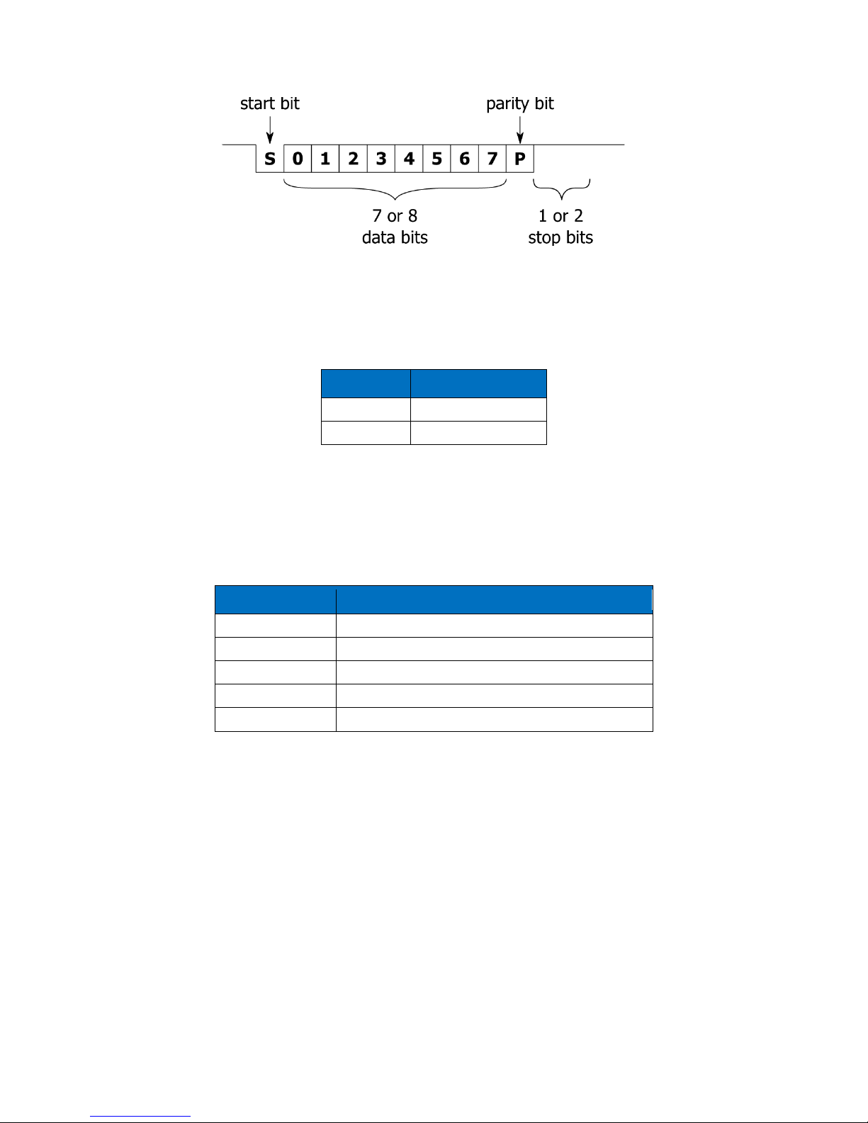
Figure 17 Modbus message frame
2.13 Data bits (40138)
Number of data bits transmitted in a single byte is determined according to the following
table:
Value
No of data bits
7
7
8 (default)
8
Table 11 Data bits
2.14 Parity bit (40139)
Each byte of data being transferred may have additional protection as a parity bit added
before stop bit (bits).
The method of calculating parity bit determines the table below:
Register value
Type of parity bit
0 (default)
none
1
Odd (number of all ones in a byte is odd)
2
Even (number of all ones in a byte is even)
3
Always 1
4
Always 0
Table 12 Parity bit
2.15 Response delay time (40140)
The value of this 16-bits register determines the number of milliseconds to wait before the
unit answers the question. This time is used to extend the interval between question and
answer. The default value of 0 means no delay (the answer is sent once during the 3.5
character required by the protocol Modbus RTU).
2.16 Watchdog time (40141)
This 16-bits register specifies the time in seconds to watchdog reset. If module does not
receive any valid message within that time, all Digital and Analog Outputs will be set to
Page 22

MINI and MIX Series I/O modules/Modbus
version 1.3 www.gc5.pl Page 22 / 73
default state.
This feature is useful if for some reason there is an interruption in data transmission and
for security reasons output states must be set to the appropriate state endanger the safety
of persons or property.
The default value is 0 seconds which means the watchdog function is disabled.
When the watchdog is triggered the Power LED blinks with the specified sequence (3 blinks
with 20Hz frequency and 1 second pause).
Page 23

MINI and MIX Series I/O modules/Modbus
version 1.3 www.gc5.pl Page 23 / 73
3 Local I/O
3.1 Universal Inputs connections
Connection of Universal Input to measure voltage 0 – 10V
Figure 18 Connection of UI to measure 0-10 VDC for MIX38 and MIX38-IP
Connection of Universal Input to measure current 0 – 20 mA
Current measurement is realized by voltage measurement and 200 Ω resistance. According
to the Ohm’s law the current is directly proportional to the voltage and the resistance as the
constant of proportionality.
According to the Ohm’s low equation for 20 mA current with 200 Ω resistance the output
voltage is 4 V. It means that the voltage 4 V on the Universal Input corresponds to 20 mA
current.
The result is expressed in millivolts.
Figure 19 Connection of UI to measure 0-20 mA for MIX38 and MIX38-IP
Page 24

MINI and MIX Series I/O modules/Modbus
version 1.3 www.gc5.pl Page 24 / 73
Connection of Universal Input to measure temperature
Figure 20 Connection of UI to measure temperature for MIX18 and MIX18-IP
Connection of Universal Input as a Digital Input (Dry Contact)
Figure 21 Connection of UI to work as DI for MIX38 and MIX38-IP
Page 25

MINI and MIX Series I/O modules/Modbus
version 1.3 www.gc5.pl Page 25 / 73
3.2 Universal Inputs MODBUS Registers
Status of Universal Inputs working as Digital Inputs (30017)
This 16-bits register contains information about the status of Digital Inputs (dry contact).
When the input is shortcut to the ground the corresponding bit value is set to 1 in
accordance with the following table:
No of bit in register
No of Universal Input
0 1 1 2 2 3 3 4 4 5 5 6 6 7 7
8
Table 13 UI register working as DI for MIX38 and MIX38-IP
Universal Input measure voltage (current) 1 - 8 (30071, 30073, 30075,
30077, 30079, 30087, 30089, 30091)
In these 16-bits registers are the results of measuring the voltage for each input. The result
is expressed in millivolts.
Measuring the current for each input results are stored in the same registers. In that case
the current value has to be calculated according to the equation:
[mA]
Universal Input measure temperature 1 - 8 (30072, 30074, 30076,
30078, 30080, 30095, 30097, 30099)
n these 16-bit registers. . The result is expressed in Celsius degrees • 10
Universal Input measure resistance 1 - 8 (30103, 30104 – 30117,
30118)
n these 32-bit registers. . The result is expressed in Ω or in 0,1 Ω for PT1000 and NI1000
configuration. In the register with lower number it is storage lower part of result and higher
register storage higher part of result.
Universal Input configuration 1 - 8 (40151 – 40158)
These 16-bit registers are used to configure Universal Inputs in accordance with the
following table:
Page 26

MINI and MIX Series I/O modules/Modbus
version 1.3 www.gc5.pl Page 26 / 73
Register value
Description
0
Off resistance measurement (only measuring the voltage, dry contact off)
1 (default)
The temperature sensor 10K3A1 NTC B=3975K
2
The temperature sensor 10K4A1 NTC B=3695K
3
The temperature sensor 10K NTC B=3435K Carel
4
The temperature sensor 20K6A1 NTC B=4262K
5
The temperature sensor 2,2K3A1 NTC B=3975K
6
The temperature sensor 3K3A1 NTC B=3975K
7
The temperature sensor 30K6A1 NTC B=4262K
8
The temperature sensor SIE1
9
The temperature sensor TAC1
10
The temperature sensor SAT1
16
The temperature sensor Pt1000
17
The temperature sensor Ni1000
+128
(set 7. bit of register)
Off voltage measurement
Table 14 Universal inputs configuration
Filter time constant of the Universal Input 1 - 8 (40159 – 40166)
These 16-bit registers consist a time constant low pass filter. The value is expressed in
seconds. Valid values must be between 0 and 60 seconds. The default filter value is 2
seconds. Setting value 0 will disable the filter.
In the case of UI shortcut or open-loop the filter is reset and UI value filtering stopped.
Resolution of the universal inputs (40167)
This register is used to determine the bit resolution for each Universal Input.
Setting the bit to 0 will set the resolution of converter to 12-bit. Setting the bit to 1 sets the
resolution of converter to 16-bit.
WARNING! Setting 16-bit resolution increases measurement time of one channel from
10 ms to 140 ms. Total time taken to measure all the channels increases from 50 ms to
700 ms.
Each input can be configured separately in accordance with the following table:
No of bit in register
No of Universal Input
0 1 1 2 2 3 3 4 4 5 5
6
Page 27

MINI and MIX Series I/O modules/Modbus
version 1.3 www.gc5.pl Page 27 / 73
6 7 7
8
Table 15 Universal inputs resolution for MIX38 and MIX38-IP
3.3 Digital Inputs Connections
Connection of Digital Input (Dry Contact)
Figure 22 Connection of DI for MIX38 and MIX38-IP
3.4 Digital Inputs MODBUS Registers
State of Digital Inputs (30016)
This 16-bit register contains the status of the Digital Inputs. Short-circuit input to GND sets
the corresponding bit in the register in accordance with the table below:
No of bit in register
No of Digital Input
0 1 1 2 … … 10
11
11
12
Table 16 Status of DI for MIX38 and MIX38-IP
Counter 1 – 12 (40023, 40024 – 40045, 40046)
The modules have 32-bit counters, one for each Digital Input.
In the register with lower number is stored lower byte of the counter and in the register with
higher number is stored higher byte of the counter.
In the case you would like to change the value of the register you can write any value (called
preset) for pulse counting registers. In the particular case, you can reset the counter by
entering 0. Reset counter is also possible via the registry 40022.
Page 28

MINI and MIX Series I/O modules/Modbus
version 1.3 www.gc5.pl Page 28 / 73
Resetting counters (40022)
Setting true value of particular bit of this 16-bit register causes reset (sets to 0) the
corresponding counter in accordance with the following table:
No of bit in register
No of Digital Input
0 1 1 2 … … 10
11
11
12
Table 17 Resetting counters for MIX38 and MIX38-IP
Setting true value of particular bit of the register causes continuously reset of the counter.
Setting the bit to 0 restores normal operation.
3.5 Analog Outputs Connections
Connection of Analog Output 0 – 10 V
Figure 23 Connection of AO for MIX38 and MIX38-IP
Connecting relay to Analog Output
Figure 24 Connection of AO to the relay for MIX38 and MIX38-IP
Page 29

MINI and MIX Series I/O modules/Modbus
version 1.3 www.gc5.pl Page 29 / 73
Connection an actuator to Analog Output
Figure 25 Connection an actuator to AO
3.6 Analog Outputs MODBUS Registers
State of Analog Outputs working as Digital Outputs (40019)
Set/setting true value of particular bit of this 16-bit register causes setting maximum output
voltage (10 V) on corresponding output and setting to 0 corresponding register with Analog
Output value (40121 – 40126).
Bits of register correspond to the following Analog Outputs.
No of bit in
register
No of Analog Output
0 1 1 2 2 3 3 4 4 5 5
6
Table 18 AO working as DO for MIX38 and MIX38-IP
Value of the analog outputs 1 – 6 (40121 – 40126)
In these 16-bit registers are stored value in mV of voltage that appears at the Analog Output.
Default state of the analog outputs (digital) (40144)
Setting true value of particular bit of this 16-bits register sets the maximum voltage (10V)
on the corresponding Analog Output after power on or watchdog reset.
Page 30

MINI and MIX Series I/O modules/Modbus
version 1.3 www.gc5.pl Page 30 / 73
Bits in register correspond to the following Analog Outputs:
No of bit in
register
No of Analog Output
0 1 1 2 2 3 3 4 4 5 5
6
Table 19 Default state of AO working as DO for MIX38 and MIX38-IP
Default state of the Analog Output 1 – 6 (40145 – 40150)
In these 16-bits registers are stored values in mV of voltage which appear on the Analog
Outputs after power on or watchdog reset.
Configuration mode of Analog Output 1 – 6 (40168 – 40173)
These 16-bit registers contain information about the mode of the Analog Outputs according
to following table:
Register
value
Description
0 (default)
Voltage output 0 – 10V
1
PWM 1Hz
2
PWM 10Hz
3
PWM 100Hz
4
PWM 0.1Hz
5
PWM 0.01Hz
Table 20 AO type settings
Hand control status of analog outputs (30015)
This register is available only for the modules with manual control of Analog Outputs.
No of bit in
register
Description
0,1
Hand status of outputs
1
2,3
Hand status of outputs
2
4,5
Hand status of outputs
3
Page 31

MINI and MIX Series I/O modules/Modbus
version 1.3 www.gc5.pl Page 31 / 73
6,7
Hand status of outputs
4
Table 21 AO Hand status bits
Value of Hand
status
Status
Description
0
AUTO
1
HAND CONTROL
Table 22 AO Hand status value
The current value of output in the hand mode determines register 30125 to 30128.
Hand control value of Analog Outputs 1 – 4 (30125 - 20128)
The registers contain a percentage value of manual control for outputs from 1 to 4.
Page 32

MINI and MIX Series I/O modules/Modbus
version 1.3 www.gc5.pl Page 32 / 73
3.7 Digital Outputs (relays) Connections
Connecting the solenoid valve to the Digital Output
Figure 26 Connection of solenoid valve to DO for MIX38 and MIX38-IP
Connecting a resistive load to the Digital Output
Figure 27Connection of resistive load to DO for MIX38 and MIX38-IP
Connecting a inductive load to the Digital Output
Figure 28 Connection of inductive load to DO for MIX38 and MIX38-IP
Page 33

MINI and MIX Series I/O modules/Modbus
version 1.3 www.gc5.pl Page 33 / 73
3.8 Digital Outputs (relays) MODBUS Registers
State of Digital Outputs (40018)
This 16-bit register contains the state of the Digital Outputs. Set/setting the particular bit in
the register enables the corresponding Digital Output according to the following table:
No of bit in
register
No of Digital Output
0 1 1 2 2 3 3 4 4 5 5
6
Table 23 State of DO for MIX38 and MIX38-IP
Default state of Digital Outputs (40143)
This 16-bit register contains the default state of the Digital Output device after the start or
watchdog reset. Register bits correspond to the Digital Outputs according to the following
table:
No of bit in
register
No of Digital Output
0 1 1 2 2 3 3 4 4 5 5
6
Table 24 Default status of DO for MIX38 and MIX38-IP
Hand control status of Digital Outputs (30015)
This register is available only for the modules with manual control of outputs.
No of bit in
register
Description
0,1
Hand status of output 1
2,3
Hand status of output 2
4,5
Hand status of output 3
6,7
Hand status of output 4
Table 25 DO Hand status bits
Page 34

MINI and MIX Series I/O modules/Modbus
version 1.3 www.gc5.pl Page 34 / 73
Value of Hand
status
Status
Description
0
AUTO
2
HAND OUT = 0
3
HAND OUT = 1
Table 26 DO Hand status value
3.9 Triac Outputs Connections
Connecting the solenoid valve to the Triac Output
Figure 28 Connection of solenoid valve to TO for 4TO-H and 4TO-H-IP
Connecting a resistive load to the Triac Output
Figure 29 Connection of resistive load to TO for 4TO-H and 4TO-H-IP
Page 35

MINI and MIX Series I/O modules/Modbus
version 1.3 www.gc5.pl Page 35 / 73
3.10 Triac Outputs MODBUS Registers
State of Triac Outputs (40018)
This 16-bit register contains the state of the Triac Outputs in digital mode. /Setting
particular bit in the register enables the corresponding Triac Output according to the
following table:
No of bit in
register
No of Triac Output
0 1 1 2 2 3 3
4
Table 27 State of TO for 4TO-H and 4TO-H-IP
Default state of triac outputs (40143)
This 16-bits register contains the default state of the Triac Output device after the start or
watchdog reset.
The register bits correspond to the Triac Outputs according to the following table:
No of bit in
register
No of Digital Output
0 1 1 2 2 3 3
4
Table 28 Default status of TO for 4TO-H and 4TO-H-IP
Value of the Triac PWM outputs 1 – 4 (40121 – 40124)
In these 16-bit registers are stored value in percent’s of duty that appears on the PWM
output. Output working mode is defined by CONFIGURATION mode of Triac Output.
Default state of the Triac PWM outputs 1 – 4 (40145 – 40148)
In these 16-bit registers are stored value in percent’s of duty that appears on the Analog
Output after power on or watchdog reset.
Configuration mode of Triac Output 1 – 4 (40168 – 40171)
These 16-bits registers contain information about the mode of the Triac Outputs according
to the following table:
Page 36

MINI and MIX Series I/O modules/Modbus
version 1.3 www.gc5.pl Page 36 / 73
Register
value
Description
1 (default)
Digital Output
2
PWM 1Hz
3
PWM 10Hz
4
Not supported
5
PWM 0.1 HZ
6
PWM 0.01Hz
Table 29 TO type settings
Hand control status of Triac Outputs (30015)
This register is available only for the modules with manual control of outputs.
No of bit in
register
Description
0,1
Hand status of outputs 1
2,3
Hand status of outputs 2
4,5
Hand status of outputs 3
6,7
Hand status of outputs 4
Table 30 TO Hand status bits
Value of Hand
status
Status
Description
0
AUTO
2
HAND OUT = 0
3
HAND OUT = 1
Table 31 TO Hand status value
Page 37

MINI and MIX Series I/O modules/Modbus
version 1.3 www.gc5.pl Page 37 / 73
3.11 Special application modes for 4I4O-H, 4I4O-H-IP, 4U4O-H and 4U4O-
H-IP
In 4I4O-H, 4I4O-H-IP, 4U4O-H, 4U4O-H-IP modules simple applications have been built which
can be used to control building devices. The applications make logic between signal from
Digital Input and control Digital Output state. Relation between Inputs and Outputs is shown
in the table below and it cannot be changed.
Digital Input
Digital Output
DI1
DO1
DI2
DO2
DI3
DO3
DI4
DO4
Table 32 Built in application relation between input and output
The Digital Inputs in modules type 4I4O-H, 4I4O-H-IP, 4U4O-H, 4U4O-H-IP can be set to work
in different modes. There are dedicated registers for operation mode (40176, 40180, 40184,
40188), time parameters (40177, 40181, 40185, 40189), setpoints for heating/cooling
modes (40178, 40182, 40186, 40190 4U4O-H and 4U4O-H-IP only) and for differential value
in heating/cooling modes (40179, 40183, 40187, 40191 4U4O-H and 4U4O-H-IP only).
Register
Description
40176
DI1 OPERATION MODE
40177
DI1 TIME VALUE
40178
DI1 SETPOINT
(4U4O-H and 4U4O-H-IP only)
40179
DI1 DIFFERENTIAL
(4U4O-H and 4U4O-H-IP only)
40180
DI2 OPERATION MODE
40181
DI2 TIME VALUE
40182
DI2 SETPOINT
(4U4O-H and 4U4O-H-IP only)
40183
DI2 DIFFERENTIAL
(4U4O-H and 4U4O-H-IP only)
40184
DI3 OPERATION MODE
40185
DI3 TIME VALUE
40186
DI3 SETPOINT
(4U4O-H and 4U4O-H-IP only)
40187
DI3 DIFFERENTIAL
(4U4O-H and 4U4O-H-IP only)
40188
DI4 OPERATION MODE
40189
DI4 TIME VALUE
Page 38

MINI and MIX Series I/O modules/Modbus
version 1.3 www.gc5.pl Page 38 / 73
40190
DI4 SETPOINT
(4U4O-H and 4U4O-H-IP only)
40191
DI4 DIFFERENTIAL
(4U4O-H and 4U4O-H-IP only)
Table 33 List of registers dedicated for special application mode
Operation Mode registers (40176,40180,40184,40188)
This register contains information about module working mode. Available modes and
register values are shown in the table below:
Value
OPERATION MODE Register
0
Ordinary IO(def)
1
Monostabile Relay
2
Bistabile Relay
3
Time Relay NO [ms]
4
Time Relay NC [ms]
5
Time Relay NO [s]
6
Time Relay NC [s]
7
Input Forwarding
8
Heating
(4U4O-H and 4U4O-H-IP only)
9
Cooling
(4U4O-H and 4U4O-H-IP only)
Table 34 Special application modes
Operating mode can be changed by writing right value in the Operation Mode register.
Special modes are initialized after 3 seconds from power-up or restart of the module (the
time value needed to stabilize the analog transmitter working).
Each Input mode change sets assigned Output to default state and reset the timer (used in
Time-based modes). When the new selected operating mode is running output is controlled
according to the new mode functioning.
3.11.1.1 Ordinary IO
In this mode, module works as a standard IO; inputs and outputs are not related which each
other.
3.11.1.2 Monostabile Relay
In this mode both rising and falling edge on digital input change output state. The action of
monostable relay can by executed remotely by changing the state of bit from false to true
in COMMAND register (40020). Outputs can by also overwritten by DIGITAL OUTPUT
register (40018), which allows remote control from BMS.
Page 39

MINI and MIX Series I/O modules/Modbus
version 1.3 www.gc5.pl Page 39 / 73
3.11.1.3 Bistabile Relay
In this mode only rising edge on digital input change output state. The action of bistable
relay can by executed remotely by changing the state of bit from false to true in COMMAND
register (40020). Outputs can by also overwritten by DIGITAL OUTPUT register (40018 ),
which allows remote control from BMS.
3.11.1.4 Time Relay NO [ms]
In this mode when the output value is false, rising edge on digital input set output to true
value. Every falling edge on digital input starts the counter from the beginning what means
that the output will stay in true value for a time defined in TIME VALUE register (expressed
in milliseconds), counting from the last falling edge of digital input. The action of time relay
can be executed remotely by changing state from false to true in relevant COMMAND
register (40020). Outputs can be also overwritten by module DIGITAL OUTPUT register
(40018), which allows to remote control from BMS.
3.11.1.5 Time Relay NC [ms]
In this mode when the output value is false, falling edge on digital input set output to true
value. Every rising edge on digital input starts the counter from the beginning what means
that the output will stay in true value for a time defined in TIME VALUE register (expressed
in milliseconds), counting from the last rising edge of digital input. The action of time relay
can be executed remotely by changing state from false to true in relevant COMMAND
register (40020). Outputs can be also overwritten by module DIGITAL OUTPUT register
(40018), which allows to remote control from BMS.
3.11.1.6 Time Relay NO [s]
In this mode when the output value is false, rising edge on digital input set output to true
value. Every falling edge on digital input starts the counter from the beginning what means
that the output will stay in true value for a time defined in TIME VALUE register (expressed
in seconds), counting from the last falling edge of digital input. The action of time relay can
be executed remotely by changing state from false to true in relevant COMMAND register
(40020). Outputs can be also overwritten by module DIGITAL OUTPUT register (40018),
which allows to remote control from BMS.
3.11.1.7 Time Relay NC [s]
In this mode when the output value is false, falling edge on digital input set output to true
value. Every rising edge on digital input starts the counter from the beginning what means
that the output will stay in true value for a time defined in TIME VALUE register (expressed
in seconds), counting from the last rising edge of digital input. The action of time relay can
be executed remotely by changing state from false to true in relevant COMMAND register
(40020). Outputs can be also overwritten by module DIGITAL OUTPUT register (40018),
which allows to remote control from BMS.
Page 40

MINI and MIX Series I/O modules/Modbus
version 1.3 www.gc5.pl Page 40 / 73
3.11.1.8 Input Forwarding
In this mode, any signal from the input is transferred directly to the assigned output without
any modifications. The input forwarding mode functioning can be stopped by Block Input
function (see Block Inputs register).
3.11.1.9 Heating mode (4U4O-H and 4U4O-H-IP only)
In this mode output is controlled as a typical thermostat, based on Setpoint register and
Control value (Input value) with differential parameter defined in Differential register. The
output signal works in 2 states low and high.
When Control value is lower or equal the difference of Setpoint register and differential
register the output is in low state.
When Control value is higher or equal the sum of Setpoint register and differential register
the output is in high state.
Output in low state:
Control value >= Setpoint + Differential
Output in high state:
Control value <= Setpoint – Differential
The heating mode algorithm is shown in chart below.
Figure 30 Heating mode algorithm functioning
WARNING! In the case when temperature sensor is failed (disconnected or shortcut) then
heating mode does not work and output stays in the false state.
Page 41

MINI and MIX Series I/O modules/Modbus
version 1.3 www.gc5.pl Page 41 / 73
3.11.1.10 Cooling mode (4U4O-H and 4U4O-H-IP only)
In this mode output is controlled as a typical thermostat, based on Setpoint register and
Control value (Input signal) with differential parameter defined in Differential register.
The output signal works in 2 states - low and high.
When Control value is lower or equal the difference of Setpoint register and Differential
register the output is in low state.
When Control value is higher or equal the sum of Setpoint register and Differential register
the output is in high state.
Output in low state:
Control value <= Setpoint – Differential
Output in high state:
Control value >= Setpoint + Differential
The cooling mode algorithm is shown in chart below.
Figure 31 Cooling mode algorithm functioning
WARNING! In the case when temperature sensor is failed (disconnected or shortcut) then
heating mode does not work and output stays in the false state.
Time Value registers (40177,40181,40185,40189)
The registers contain time values for TIME RELAY modes. The time unit depends on
selected mode [milliseconds] or [seconds].
Page 42

MINI and MIX Series I/O modules/Modbus
version 1.3 www.gc5.pl Page 42 / 73
Command register (40020)
The module have special register COMMAND (40020). The command register is used for
remotely execute action ( simulate light switch/PIR). The action is executed by changing
state of relevant bit (changing from false to true). All special application modes can be
executed except Input Forwarding, Heating and Cooling modes.
No of bit in register
(40020)
Command input
number
0 1 1 2 2 3 3
4
Table 32 Command register for special application modes
Block Inputs register (40021)
The Block Inputs register is used to block physical input signals to take action in logic. By
setting true value on relevant bit the module block input and no action will be executed.
Setting false value restores normal operation. The block input function does not work when
the heating/cooling input mode is set.
No of bit in register
(40021)
Block input
number
0 1 1 2 2 3 3
4
Table 35 Block inputs register.
Setpoint registers (40178,40182,40186,40190)
The SETPOINT registers contain values which are used in heating/cooling modes (4U4O-H
and 4U4O-H-IP only) as the setpoints for heating/cooling control algorithm
The default Setpoint value is 21. (read more in Heating mode, Cooling mode).
The register stores the setpoint multiplied by 10.
Differential registers (40179,40183,40187,40191)
The DIFFERENTIAL registers contain values which are used in heating/cooling modes
(4U4O-H and 4U4O-H-IP only) as the differential for heating/cooling control algorithm.
Setpoint registers and Differential registers create deadband of the Control values which
has no influence on output.
Deadband = (Setpoint – Differential, Setpoint + Differential)
Page 43

MINI and MIX Series I/O modules/Modbus
version 1.3 www.gc5.pl Page 43 / 73
The default Differential value is 1. (read more in Heating mode, Cooling mode).
The register stores the differential multiplied by 10.
4 WEB Configuration- only IP version
4.1 Web server access
All IP version modules have built in web server, which allows to show module status and to
change configuration.
To access web server open browser and entre IP address of the module, default address
for new module ( default IP address is 192.168.1.123 ). Please use the following credentials :
Username: platform
Password: 1000 ( by default )
4.2 Device page
This page contains information and technical specification of the device. The Basic
Information section includes information about module type, firmware version and uptime.
In the Device Specification there are information about: Power Supply, Inputs / Outputs
parameters, Interfaces and Mechanical.
Figure 32 Device page of 8U-IP
Page 44

MINI and MIX Series I/O modules/Modbus
version 1.3 www.gc5.pl Page 44 / 73
4.3 Local I/O status and configuration
Universal Inputs
This page allows to enter configuration parameters and show actual value of Universal
Inputs. To open this page please navigate to Local IO tab and choose Universal Inputs from
submenu.
Figure 30 Universal Inputs page of 8U-IP
•
Figure 34 Types of sensors
Universal Input table has the following fields:
• Sensor type (Read & Write) allows to set different type of sensor.
• Resolution (Read & Write), resolution measurement 12bits / 16bits (for PT1000 and
Ni1000 sensors please use 16bits).
• UI Flag (Read Only), status of UI as DI.
• Disable Voltage Measurement (Read & Write), disable voltage measuring for resistance
measurement only.
• L.P. Filter Constant (Read & Write),parameter time constant low pass filter in seconds.
Valid values must be between 0 and 60 seconds (default 2s). Setting value 0 will
disable the filter.
• Resistance (Read Only), in ohms from 0 to 1000k [Ω].
Page 45

MINI and MIX Series I/O modules/Modbus
version 1.3 www.gc5.pl Page 45 / 73
• Temperature (Read Only), in Celsius with an accuracy of 1 decimal [°C].
• Voltage (Read Only) in millivolts [mV].
WARNING! To save changes please use “Submit” button
.
Special application modes configuration
This page allows to enter configuration parameters and show actual value of Special
application modes. To open this page please navigate to Local IO tab and choose Universal
Inputs from submenu.
Figure 35 Universal Inputs page of 4U4O-IP
Figure 36 Special application modes
Special Modes Configuration table has the following fields:
• Block Input (Read & Write) allows to block particular input (except heating/cooling
modes).
• Input Mode (Read & Write), allows to select the Special Application Mode for particular
input (Ordinary IO in default).
• Command (Read & Write), execution of the Special Application Modes (except input
forwarding, heating/cooling modes).
• Mode Time (Read & Write), Time base for time relay application modes (unit depends
on selected mode [ms] or [s]).
• Setpoint (Read & Write, 4U4O-H-IP only), setpoint value for heating/cooling modes.
Page 46

MINI and MIX Series I/O modules/Modbus
version 1.3 www.gc5.pl Page 46 / 73
In default 0.
• Differential (Read & Write, 4U4O-H-IP only), differential value for heating/cooling modes.
In default 0.
WARNING! To save changes please use “Submit” button
.
Digital Inputs
This page allows to enter configuration parameters and shows actual value of Digital
Inputs. To open this page please navigate to Local IO tab and choose Digital Inputs from
submenu.
Figure 37 Digital Inputs page of MIX38-IP
Digital Input table has the following fields:
• State (Read Only), actual input state.
• Reset Flag (Read & Write), reset of pulses value (leaving reset active will case resetting
pulses value).
• Counter State (Read Only), actual value of pulses save in EEPROM.
• Counter State To Set (Read & Write ), allows to set value of counter.
WARNING! To save changes please use “Submit” button
.
Digital Outputs
This page allows to enter configuration parameters and shows actual value of Digital
Outputs. To open this page please navigate to Local IO tab and choose Digital Outputs from
submenu.
Page 47

MINI and MIX Series I/O modules/Modbus
version 1.3 www.gc5.pl Page 47 / 73
Figure 38 Digital Outputs page of MIX38-IP
Digital Outputs table has the following fields:
• State (Read & Write), actual state of digital output.
• Default State (Read & Write), output state after power up and watchdog.
• Watchdog (Read & Write),device watchdog value in seconds.
WARNING! To save changes please use “Submit” button
.
Analog Outputs
This page allows to enter configuration parameters and shows actual value of Analog
Outputs. To open this page please navigate to Local IO tab and choose Analog Outputs from
submenu.
Figure 39 Analog Outputs page of 4U4A-H-IP
Analog Outputs table has the following fields:
• Value (Read & Write), actual value of analog output in millivolts [mV].
• Type (Read & Write), analog output working mode voltage / PWM.
• Default Value (Read & Write). default output value after power up and watchdog.
• Digital Output (Read & Write). output status flag for DO mode.
• Default Digital Output (Read & Write). default output status for DO mode.
• Watchdog (Read & Write), device watchdog value in seconds.
Page 48

MINI and MIX Series I/O modules/Modbus
version 1.3 www.gc5.pl Page 48 / 73
• Hand State Output (Read Only, MINI series only), manual overrides potentiometer
status
WARNING! To save changes please use “Submit” button
.
4.4 RS485 Configuration
This page allow to enter configuration parameters and show information of controllers
RS485 port.
Figure 40 RS485 configuration page
This page allows to set parameters such as:
• Baud rate (Read Only ), RS485 baud rate from 2400 up to 115200.
• Modbus Config (Read Only ), Modbus Protocol Type- RTU or ASCII.
• Stop Bits (Read & Write), number of stop bits (1 or 2).
• Data Bits (Read & Write), number of data bits transmitted in a single byte
(7 or 8).
• Parity Bits (Read & Write), transmission protection as a parity bit added before stop bit
(bits).
• RS485 Biasing Resistors , biasing resistors activation only for MINI modules with a
hardware version >= 2.0 (option unavailable in MIX modules)
• Received Frames (Read Only), number of received frames.
• Transmitted Frames (Read Only), number of transmitted frames.
• Error Frames (Read Only), number of error frames.
WARNING! To save changes please use “Submit” button
.
Page 49

MINI and MIX Series I/O modules/Modbus
version 1.3 www.gc5.pl Page 49 / 73
4.5 IP Configuration
This page allows to change parameters of Ethernet port, Modbus TCP and BACnet IP.
Figure 41 IP configuration page
This page allows to set parameters such as:
• IP Address (Read & Write), controller Ethernet interface IP address.
• Mask (Read & Write), network mask.
• Gateway (Read & Write), network default gateway.
• Http Port (Read & Write), http port.
• Mac Address (Read Only), Ethernet interface MAC address.
• Protocol Type (Read Only), Dip Switch protocol selection.
• Modbus TCP Port (Read & Write), Modbus TCP port number, default 502.
• Modbus Address (Read Only). Modbus device address set by rotary switches.
• Modbus TCP Communication Timeout (Read & Write), timeout for TCP/IP messages.
• RS485 Timeout (Read & Write), timeout for Modbus RTU/ASCII messages.
• Send Modbus Errors (Read Only), Enable / Disable sending Modbus error messages.
• BACnet ID (Read & Write), BACnet ID set by rotary switches, this value can be
overridden by the user, once overridden by user changing rotary switches will not affect
BACnet ID.
• BACnet UDP port (Read & Write),BACnet IP port.
WARNING! To save changes please first click “Submit” button and then “Reboot” button
Page 50

MINI and MIX Series I/O modules/Modbus
version 1.3 www.gc5.pl Page 50 / 73
4.6 Device management
This page allows to change password and remote reboot device.
Figure 42 Device management page
Procedure of changing device password:
a) enter current device password in field - Current Device Password,
b) enter new device password in field - New Device Password,
c) enter again new device password in field - Confirm New Device Password,
d) to confirm password change please click “Submit” button,
e) please Logout and Login again using new password.
WARNING! To reset password to default refer to “Restoring default settings”
4.7 Contact
This page displays information about Manufacture web address and email to technical
support.
Figure 43 Contact page view
Page 51

MINI and MIX Series I/O modules/Modbus
version 1.3 www.gc5.pl Page 51 / 73
5 Modbus TCP/IP modules
5.1 Modbus TCP/IP
The device simultaneously supports up to 4 Modbus TCP clients. If the fifth device will want
to connect to the module, TCP connection will be rejected. In order to secure the module
before filling up the call list, it was introduced a mechanism for monitoring each Modbus
TCP connection. There is a parameter called Modbus TCP Communication Timeout
(default 60s), If during this time will not come any request from the Modbus TCP client,
module will close the connection.
To read internal registers of the module need to generate the correct MODBUS TCP frame
with address according to the setting of dipswitch, If the address is different the frame will
be sent to the RS485 port.
If module receive an incorrect MODBUS TCP frame, it sends back a frame with error code:
0x01 - if the function code in the query is not supported
0x02 - if the address of the register is invalid
0x03 - If in the query disagrees the amount of data
If the query is correct, device instantly generates answer with the data or acknowledgment
of receipt of data, depending on the query.
5.2 Module as Modbus TCP/IP Gateway to RS485
All IP version modules have built in Modbus TCP/IP to RS485 gateway which allows to
connects using RS485 an additional I/O modules or 3rd party Modbus devices. In order to
ensure proper operation of Modbus Gateway please make sure that all parameters of
RS485 ( Baud Rate, Stop Bits ect.) of all the devices connected to RS485 ( Gateway and an
addition I/O modules/devices) are same.
Operation of gateway is based on checking the MODBUS address in the MODBUS TCP
query. If the address is different from the set on the dipswitch, data frame from query is
converted to MODBUS RTU/ASCII, and sent to the RS485 port. Then the module waits for
an answer from device connected to the RS485, if slave does not respond within the
estimated time defined by the RS485 Timeout (default 500ms), an exception response will
be given: error code 0x0B. If the slave answered the correct frame, it is converted to Modbus
TCP and sent to the master.
Module in gateway functionality in case of not receive valid frame, send error code 0x0B.
Some systems upon receipt of this error code, no repeats the query according to the
settings. No retry may result in immediate going point to down mode. That is why modules
have the ability to block the sending information about errors (Send Modbus Errors setting
from built in web or iSMA-Configurator). Then in the absence of any response, the system
retry the request according to the settings.
Page 52

MINI and MIX Series I/O modules/Modbus
version 1.3 www.gc5.pl Page 52 / 73
Figure 44 Modbus TCP/IP to RS485 Gateway an example
Page 53

MINI and MIX Series I/O modules/Modbus
version 1.3 www.gc5.pl Page 53 / 73
6 List of all Modbus Registers
Below is a table with all the registers available for all types of modules. Please notice that
for some types of modules some of the registers are not available according to the physical
number and types of Inputs and Outputs.
Modbus
Addr
Dec
Addr
Hex
Addr
Register name
Access
Description
30001
0
0x00
VERSION AND MODULE
TYPE
Read Only
30002
1
0x01
MODULE ADDRESS (state
of switch)
Read Only
30003
2
0x02
BAUD RATE AND
PROTOCOL
(state of switch)
Read Only
30004
3
0x03
COUNTER OF RECEIVED
FRAMES (32 – bits)
Read Only
Default state is 0 Reset at the unit start
and change of transmission
parameters.
30006
5
0x05
COUNTER OF FRAMES
WITH ERROR (32 – bits)
Read Only
Default state is 0 Reset at the unit start
and change of transmission
parameters.
30008
7
0x07
COUNTER OF SENT
FRAMES
(32 – bits)
Read Only
Default state is 0 Reset at the unit start
and change of transmission
parameters.
30015
14
0xE
STATUS OF MANUAL
OPERATION
Read Only
Status of manual operation DO, TO and
AO for modules MINI series
30016
15
0x0F
STATE OF DIGITAL INPUTS
Read Only
30017
16
0x10
STATE OF UNIVERSAL
INPUTS
WORKING AS DIGITAL
INPUTS
Read Only
Status of Universal Inputs working as
digital inputs
40001
0
0x00
DEVICE ACTIONS
Read &
Write
Allows to enable 1 of 3 device actions
40018
17
0x11
STATE OF DIGITAL
OUTPUTS
Read &
Write
State of Digital Outputs
40019
18
0x12
STATE OF ANALOG
OUTUTS
WORKING AS DIGITAL
OUTPUTS
Read &
Write
State of Analog Outputs working as
Digital Outputs
40020
19
0x13
DIGITAL INPUTS
COMMAND REGISTER
Read &
Write
Digital Inputs command register
40021
20
0x14
DIGITAL INPUTS
BLOCKING
Read &
Write
Digital Inputs blocking register
40022
21
0x15
COUNTER RESET
Read &
Set bit in register to reset corresponding
Page 54

MINI and MIX Series I/O modules/Modbus
version 1.3 www.gc5.pl Page 54 / 73
Modbus
Addr
Dec
Addr
Hex
Addr
Register name
Access
Description
Write
counter.
40023
22
0x16
COUNTER 1 LSB
Read &
Write
Memory
32-bit counters for each Digital Input
counting pulses.
40024
23
0x17
COUNTER 1 MSB
40025
24
0x18
COUNTER 2 LSB
Read &
Write
Memory
40026
25
0x19
COUNTER 2 MSB
40027
26
0x1A
COUNTER 3 LSB
Read &
Write
Memory
40028
27
0x1B
COUNTER 3 MSB
40029
28
0x1C
COUNTER 4 LSB
Read &
Write
Memory
40030
29
0x1D
COUNTER 4 MSB
40031
30
0x1E
COUNTER 5 LSB
Read &
Write
Memory
40032
31
0x1F
COUNTER 5 MSB
40033
32
0x20
COUNTER 6 LSB
Read &
Write
Memory
40034
33
0x21
COUNTER 6 MSB
40035
34
0x22
COUNTER 7 LSB
Read &
Write
Memory
40036
35
0x23
COUNTER 7 MSB
40037
36
0x24
COUNTER 8 LSB
Read &
Write
Memory
40038
37
0x25
COUNTER 8 MSB
40039
38
0x26
COUNTER 9 LSB
Read &
Write
Memory
40040
39
0x27
COUNTER 9 MSB
40041
40
0x28
COUNTER 10 LSB
Read &
Write
Memory
40042
41
0x29
COUNTER 10 MSB
40043
42
0x2A
COUNTER 11 LSB
Read &
Write
Memory
40044
43
0x2B
COUNTER 11 MSB
40045
44
0x2C
COUNTER 12 LSB
Read &
Write
Memory
40046
45
0x2D
COUNTER 12 MSB
30071
70
0x46
UIVERSAL INPUT VOLTAGE
1
Read Only
Voltage measurement value is
expressed in mV.
30072
71
0x47
UIVERSAL INPUT
TEMPERATURE 1
Read Only
Page 55

MINI and MIX Series I/O modules/Modbus
version 1.3 www.gc5.pl Page 55 / 73
Modbus
Addr
Dec
Addr
Hex
Addr
Register name
Access
Description
30073
72
0x48
UIVERSAL INPUT VOLTAGE
2
Read Only
Formula for the current measurements:
where: U – register value,
500 – value of attached resistor
Temperature is expressed in Celsius
degrees * 10
For a result, divide the registry value by
10:
Selection of the type sensor is done
using UNIVERSAL INPUT
CONFIGURATION register from 40151
to 40158 for each input separately
30074
73
0x49
UIVERSAL INPUT
TEMPERATURE 2
Read Only
30075
74
0x4A
UIVERSAL INPUT VOLTAGE
3
Read Only
30076
75
0x4B
UIVERSAL INPUT
TEMPERATURE 3
Read Only
30077
76
0x4C
UIVERSAL INPUT VOLTAGE
4
Read Only
30078
77
0x4D
UIVERSAL INPUT
TEMPERATURE 4
Read Only
30079
78
0x4E
UIVERSAL INPUT VOLTAGE
5
Read Only
30080
79
0x4F
UIVERSAL INPUT
TEMPERATURE 5
Read Only
30081
80
0x50
UIVERSAL INPUT VOLTAGE
6
Read Only
30082
81
0x51
UIVERSAL INPUT
TEMPERATURE 6
Read Only
30083
82
0x52
UIVERSAL INPUT VOLTAGE
7
Read Only
30084
83
0x53
UIVERSAL INPUT
TEMPERATURE 7
Read Only
30085
84
0x54
UIVERSAL INPUT VOLTAGE
8
Read Only
30086
85
0x55
UIVERSAL INPUT
TEMPERATURE 8
Read Only
30087
86
0x56
UIVERSAL INPUT VOLTAGE
1
Read Only
30088
87
0x57
UIVERSAL INPUT VOLTAGE
2
Read Only
30089
88
0x58
UIVERSAL INPUT VOLTAGE
3
Read Only
30090
89
0x59
UIVERSAL INPUT VOLTAGE
4
Read Only
30091
90
0x5A
UIVERSAL INPUT VOLTAGE
5
Read Only
30092
91
0x5B
UIVERSAL INPUT VOLTAGE
6
Read Only
30093
92
0x5C
UIVERSAL INPUT VOLTAGE
Read Only
Page 56

MINI and MIX Series I/O modules/Modbus
version 1.3 www.gc5.pl Page 56 / 73
Modbus
Addr
Dec
Addr
Hex
Addr
Register name
Access
Description
7
30094
93
0x5D
UIVERSAL INPUT VOLTAGE
8
Read Only
30095
94
0x5E
UIVERSAL INPUT
TEMPERATURE 1
Read Only
30096
95
0x5F
UIVERSAL INPUT
TEMPERATURE 2
Read Only
30097
96
0x60
UIVERSAL INPUT
TEMPERATURE 3
Read Only
30098
97
0x61
UIVERSAL INPUT
TEMPERATURE 4
Read Only
30099
98
0x62
UIVERSAL INPUT
TEMPERATURE 5
Read Only
30100
99
0x63
UIVERSAL INPUT
TEMPERATURE 6
Read Only
30101
100
0x64
UIVERSAL INPUT
TEMPERATURE 7
Read Only
30102
101
0x65
UIVERSAL INPUT
TEMPERATURE 8
Read Only
30103
102
0x66
RESISTIVE INPUT 1 LSB
Read Only
Resistance measurement result
expressed in Ω
30104
103
0x67
RESISTIVE INPUT 1 MSB
Read Only
30105
104
0x68
RESISTIVE INPUT 2 LSB
Read Only
30106
105
0x69
RESISTIVE INPUT 2 MSB
Read Only
30107
106
0x6A
RESISTIVE INPUT 3 LSB
Read Only
30108
107
0x6B
RESISTIVE INPUT 3 MSB
Read Only
30109
108
0x6C
RESISTIVE INPUT 4 LSB
Read Only
30110
109
0x6D
RESISTIVE INPUT 4 MSB
Read Only
30111
110
0x6E
RESISTIVE INPUT 5 LSB
Read Only
30112
111
0x6F
RESISTIVE INPUT 5 MSB
Read Only
30113
112
0x70
RESISTIVE INPUT 6 LSB
Read Only
30114
113
0x71
RESISTIVE INPUT 6 MSB
Read Only
30115
114
0x72
RESISTIVE INPUT 7 LSB
Read Only
30116
115
0x73
RESISTIVE INPUT 7 MSB
Read Only
30117
116
0x74
RESISTIVE INPUT 8 LSB
Read Only
30118
117
0x75
RESISTIVE INPUT 8 MSB
Read Only
40121
120
0x78
VALUE OF ANALOG
OUTPUT 1
Read &
Write
The voltage at the Analog Outputs given
40122
121
0x79
VALUE OF ANALOG
Read &
Page 57

MINI and MIX Series I/O modules/Modbus
version 1.3 www.gc5.pl Page 57 / 73
Modbus
Addr
Dec
Addr
Hex
Addr
Register name
Access
Description
OUTPUT 2
Write
in the mV range from 0 to 10000mV
40123
122
0x7A
VALUE OF ANALOG
OUTPUT 3
Read &
Write
40124
123
0x7B
VALUE OF ANALOG
OUTPUT 4
Read &
Write
40125
124
0x7C
VALUE OF ANALOG
OUTPUT 5
Read &
Write
40126
125
0x7D
VALUE OF ANALOG
OUTPUT 6
Read &
Write
30125
124
0x7C
HAND STATUS VALUE 1
Read Only
The current value of Analog Output in
the hand mode for MINI with AO
30126
125
0x7D
HAND STATUS VALUE 2
Read Only
30127
126
0x7E
HAND STATUS VALUE 3
Read Only
30128
127
0x7F
HAND STATUS VALUE 4
Read Only
30130
129
0x81
HARDWARE_VERSION
Read Only
The current hardware version of a
device
30131
130
0x82
MAC_ADDRESS (32 – bits)
Read Only
The MAC address of a device
40136
135
0x87
BAUD RATE
Read &
Write
Memory
Transmission speed is defined by the
user calculated using the formula:
The value is considered only when
sections 1, 2 and 3 of S3 switch is in the
OFF position
The default value is 7680 (76800 bps)
40137
136
0x88
STOP BITS
Read &
Write
Memory
Supported values are 1 and 2
The default value 1
40138
137
0x89
DATA BITS
Read &
Write
Memory
Supported values are 7 and 8
The default value 8
40139
138
0x8A
PARITY BIT
Read &
Write
Memory
Parity bit (40139) The default value is 0
(no parity)
Allowed values:
Value
Description
0 (default)
none
1
Odd 2 Even
3
Always 1
4
Always 0
40140
139
0x8B
RESPONSE DELAY
Read &
Write
Delay in ms before sending response
The default value is 0.
Page 58

MINI and MIX Series I/O modules/Modbus
version 1.3 www.gc5.pl Page 58 / 73
Modbus
Addr
Dec
Addr
Hex
Addr
Register name
Access
Description
Memory
40141
140
0x8C
WATCHDOG TIME
Read &
Write
Memory
Time in second before watchdog reset
in case no transmission.
A value of 0 disables Watchdog.
The default value is 0s
40143
142
0x8E
DEFAULT STATE OF
DIGITAL OUTPUTS
Read &
Write
Memory
State of Digital Outputs assigned at the
start of the module and watchdog reset.
The default value is 0.
40144
143
0x8F
DEFAULT STATE OF
ANALOG OUTPUTS
(DIGITAL)
Read &
Write
Memory
State of Analog Outputs assigned at the
start of the module and watchdog reset.
The default value is 0.
40145
144
0x90
DEFAULT STATE OF
ANALOG OUTPUT 1
Read &
Write
Memory
In the registers is stored value that
appears at the Analog Output after
power on or watchdog reset.
The default value is 0.
40146
145
0x91
DEFAULT STATE OF
ANALOG OUTPUT 2
Read &
Write
Memory
40147
146
0x92
DEFAULT STATE OF
ANALOG OUTPUT 3
Read &
Write
Memory
40148
147
0x93
DEFAULT STATE OF
ANALOG OUTPUT 4
Read &
Write
Memory
40149
148
0x94
DEFAULT STATE OF
ANALOG OUTPUT 5
Read &
Write
Memory
40150
149
0x95
DEFAULT STATE OF
ANALOG OUTPUT 6
Read &
Write
Memory
40151
150
0x96
UNIVERSAL INPUT
CONFIGURATION 1
Read &
Write
Memory
Configuration of Universal Input and
type of temperature sensor.
The default value is 1.
Valu
e
Description / Sensor
0
Resistance
measurement off
1
10K3A1 NTC
2
10K4A1 NTC
3
10K NTC Carel
40152
151
0x97
UNIVERSAL INPUT
CONFIGURATION 2
Read &
Write
Memory
40153
152
0x98
UNIVERSAL INPUT
CONFIGURATION 3
Read &
Write
Memory
40154
153
0x99
UNIVERSAL INPUT
CONFIGURATION 4
Read &
Write
Memory
40155
154
0x9A
UNIVERSAL INPUT
Read &
Page 59

MINI and MIX Series I/O modules/Modbus
version 1.3 www.gc5.pl Page 59 / 73
Modbus
Addr
Dec
Addr
Hex
Addr
Register name
Access
Description
CONFIGURATION 5
Write
Memory
4 20K6A1 NTC
5
2,2K3A1 NTC B=3975K
6
3K3A1 NTC
7
30K6A1 NTC
8
SIE1
9
TAC1
10
SAT1
16
Pt1000
17
Ni1000
+128
Voltage measurement
off
40156
155
0x9B
UNIVERSAL INPUT
CONFIGURATION 6
Read &
Write
Memory
40157
156
0x9C
UNIVERSAL INPUT
CONFIGURATION 7
Read &
Write
Memory
40158
157
0x9D
UNIVERSAL INPUT
CONFIGURATION 8
Read &
Write
Memory
40159
158
0x9E
FILTER TIME CONSTANT
OF THE UNIVERSAL INPUT
1
Read &
Write
Memory
Filter time constant, expressed in
seconds in the range from 0 to 60
seconds.
A value of 0 disables the filter.
The default value is 2s.
40160
159
0x9F
FILTER TIME CONSTANT
OF THE UNIVERSAL INPUT
2
Read &
Write
Memory
40161
160
0xA0
FILTER TIME CONSTANT
OF THE UNIVERSAL INPUT
3
Read &
Write
Memory
40162
161
0xA1
FILTER TIME CONSTANT
OF THE UNIVERSAL INPUT
4
Read &
Write
Memory
40163
162
0xA2
FILTER TIME CONSTANT
OF THE UNIVERSAL INPUT
5
Read &
Write
Memory
40164
163
0xA3
FILTER TIME CONSTANT
OF THE UNIVERSAL INPUT
6
Read &
Write
Memory
40165
164
0xA4
FILTER TIME CONSTANT
OF THE UNIVERSAL INPUT
7
Read &
Write
Memory
40166
165
0xA5
FILTER TIME CONSTANT
OF THE UNIVERSAL INPUT
8
Read &
Write
Memory
40167
166
0xA6
RESOLUTION OF THE
UNIVERSAL INPUTS
Read &
Write
Memory
Resolution of Analog Inputs. When bit is
set measurement at corresponding
input is done with 16-bit resolution.
By default, all measurements are done
Page 60

MINI and MIX Series I/O modules/Modbus
version 1.3 www.gc5.pl Page 60 / 73
Modbus
Addr
Dec
Addr
Hex
Addr
Register name
Access
Description
with 12-bit resolution.
40168
167
0xA7
ANALOG OUTPUT
CONFIGURATION 1
Read &
Write
Memory
Configuring the mode of Analog Output
according to the following table:
Value
Description
0 (default)
Voltage output 0-10V
1
PWM 1Hz
2
PWM 10Hz
3
PWM 100Hz
4
PWM 0.1Hz
5
PWM 0.01Hz
40169
168
0xA8
ANALOG OUTPUT
CONFIGURATION 2
Read &
Write
Memory
40170
169
0xA9
ANALOG OUTPUT
CONFIGURATION 3
Read &
Write
Memory
40171
170
0xAA
ANALOG OUTPUT
CONFIGURATION 4
Read &
Write
Memory
40172
171
0xAB
ANALOG OUTPUT
CONFIGURATION 5
Read &
Write
Memory
40173
172
0xAC
ANALOG OUTPUT
CONFIGURATION 6
Read &
Write
Memory
40176
175
0xAF
DIGITAL INPUT 1
CONFIGURATIO MODE
Read &
Write
Memory
DIGITAL INPUT CONFIGURATIO MODE
table:
Value
Description
0
Ordinary IO
1
Monostable Relay
2
Bistable Relay
3
Time Relay
DIGITAL INPUT TIME VALUE in [ms] or
in [s] – depends on mode selection
SETPOINT in oC multiplied by 10
Default value = 0
40177
176
0xB0
DIGITAL INPUT 1
TIME VALUE
Read &
Write
Memory
40178
177
0xB1
DIGITAL INPUT 1
SETPOINT
Read &
Write
Memory
40179
178
0xB2
DIGITAL INPUT 1
DIFFERENTIAL
Read &
Write
Memory
40180
179
0xB3
DIGITAL INPUT 2
CONFIGURATIO MODE
Read &
Write
Memory
40181
180
0xB4
DIGITAL INPUT 2
TIME VALUE
Read &
Write
Memory
40182
181
0xB5
DIGITAL INPUT 2
SETPOINT
Read &
Write
Memory
40183
182
0xB6
DIGITAL INPUT 2
DIFFERENTIAL
Read &
Write
Memory
Page 61

MINI and MIX Series I/O modules/Modbus
version 1.3 www.gc5.pl Page 61 / 73
Modbus
Addr
Dec
Addr
Hex
Addr
Register name
Access
Description
40184
183
0xB7
DIGITAL INPUT 3
CONFIGURATIO MODE
Read &
Write
Memory
DIFFERENTIAL in oC multiplied by 10
Default value = 0
40185
184
0XB8
DIGITAL INPUT 3
TIME VALUE
Read &
Write
Memory
40186
185
0xB9
DIGITAL INPUT 3
SETPOINT
Read &
Write
Memory
40187
186
0xBA
DIGITAL INPUT 3
DIFFERENTIAL
Read &
Write
Memory
40188
187
0xBB
DIGITAL INPUT 4
CONFIGURATIO MODE
Read &
Write
Memory
40189
188
0xBC
DIGITAL INPUT 4
TIME VALUE
Read &
Write
Memory
40190
189
0xBD
DIGITAL INPUT 4
SETPOINT
Read &
Write
Memory
40191
190
0xBE
DIGITAL INPUT 4
DIFFERENTIAL
Read &
Write
Memory
Page 62

MINI and MIX Series I/O modules/Modbus
version 1.3 www.gc5.pl Page 62 / 73
7 List of supported temperature sensors
No 1 No
2
Sensor
10K3A1
Sensor
10K4A1
β coeffictient
3975K
β coeffictient
3695K
Manufacturers
Aquatrol, Cylon, Honeywell,
Johnson, Satchwell,
Seachange
Manufacturers
Andover, Delta
Controls, Siebe, York
°C Ω °C
Ω
-50
667828
-50
441667
-45
491749
-45
330749
-40
335671
-40
239831
-35
241840
-35
181532
-30
176683
-30
135233
-25
131251
-25
105081
-20
96974
-20
78930
-15
72895
-15
61030
-10
55298
-10
47549
-5
42314
-5
37316 0 32650
0
29490 5 25396
5
23462
10
19904
10
18787
15
15714
15
15136
20
12494
20
12268
25
10000
25
10000
30
8056
30
8197
35
6530
35
6754
40
5325
40
5594
45
4367
45
4656
50
3601
50
3893
55
2985
55
3271
60
2487
60
2760
65
2082
65
2339
70
1751
70
1990
75
1480
75
1700
80
1256
80
1458
85
1070
85
1255
Page 63

MINI and MIX Series I/O modules/Modbus
version 1.3 www.gc5.pl Page 63 / 73
No 1 No
2
90
916
90
1084
95
787
95
939
100
678
100
817
105
587
105
713
110
510
110
624
115
444
115
547
120
388
120
482
125
340
125
426
Page 64

MINI and MIX Series I/O modules/Modbus
version 1.3 www.gc5.pl Page 64 / 73
No 3 No
4
Sensor
10K Carel
Sensor
20K6A1
β coeffictient
3435K
β coeffictient
4262K
°C
Ω
Manufacturers
Honeywell
-50
329500
°C
Ω
-45
247700
-40
806800
-40
188500
-35
574400
-35
144100
-30
413400
-30
111300
-25
300400
-25
86430
-20
220600
-20
67770
-15
163480
-15
53410
-10
122260
-10
42470
-5
92220
-5
33900
0
70140 0 27280
5
53780 5 22050
10
41540
10
17960
15
32340
15
14690
20
25340
20
12090
25
20000
25
10000
30
15886
30
8313
35
12698
35
6940
40
10212
40
5827
45
8260
45
4912
50
6718
50
4161
55
5494
55
3536
60
4518
60
3020
65
3732
65
2588
70
3098
70
2228
75
2586
75
1924
80
2166
80
1668
85
1823
85
1451
90
1541
90
1266
95
1308
95
1108
100
1114
100
973
105
953
105
857
110
818
Page 65

MINI and MIX Series I/O modules/Modbus
version 1.3 www.gc5.pl Page 65 / 73
No 3 No
4
110
758
115
704
115
672
120
609
120
597
125
528
125
531
Page 66

MINI and MIX Series I/O modules/Modbus
version 1.3 www.gc5.pl Page 66 / 73
No 5 No
6
Sensor
2.2K3A1
Sensor
3K3A1
β coeffictient
3975K
β coeffictient
3975K
Manufacturers
Ambiflex, Johnson
Manufacturers
Alerton
°C Ω °C
Ω
-50
329500
-50
200348
-45
247700
-45
150524
-40
188500
-40
100701
-35
144100
-35
76853
-30
111300
-30
53005
-25
86430
-25
41048
-20
67770
-20
29092
-15
53410
-15
21868
-10
42470
-10
16589
-5
33900
-5
12694 0 27280
0
9795 5 22050
5
7619
10
17960
10
5971
15
14690
15
4714
20
12090
20
3748
25
10000
25
3000
30
8313
30
2417
35
6940
35
1959
40
5827
40
1598
45
4912
45
1310
50
4161
50
1080
55
3536
55
896
60
3020
60
746
65
2588
65
625
70
2228
70
526
75
1924
75
444
80
1668
80
377
85
1451
85
321
90
1266
90
275
95
1108
95
236
100
973
100
204
Page 67

MINI and MIX Series I/O modules/Modbus
version 1.3 www.gc5.pl Page 67 / 73
No 5 No
6
105
857
105
176
110
758
110
153
115
672
115
133
120
597
120
117
125
531
125
102
Page 68

MINI and MIX Series I/O modules/Modbus
version 1.3 www.gc5.pl Page 68 / 73
No 7 No
8
Sensor
30K6A1
Sensor
SIE1
β coeffictient
4262K
Manufacturers
Barber Colman, Siebe
Manufacturers
Drayton
°C Ω °C
Ω
-50
10732
-30
622911
-45
10624
-25
477393
-40
10517
-20
331876
-35
10344
-15
245785
-30
10172
-10
183697
-25
9913
-5
138502
-20
9654 0 105305
-15
9320 5 60713
-10
8933
10
62347
-5
8496
15
48511
0
8044
20
38019
5
7489
25
30000
10
6938
30
23828
15
6370
35
19046
20
5798
40
15317
25
5238
45
12390
30
4696
50
10079
35
4185
55
8243
40
3707
60
6777
45
3271
65
5600
50
2875
70
4650
55
2521
75
3879
60
2206
80
3251
65
1929
85
2737
70
1685
90
2313
75
1472
95
1963
80
1287
100
1672
85
1127
105
1430
90
986
110
1228
95
866
115
1058
100
760
120
915
105
670
Page 69

MINI and MIX Series I/O modules/Modbus
version 1.3 www.gc5.pl Page 69 / 73
No 7 No
8
125
793
110
590
115
522
120
462
125
410
Page 70

MINI and MIX Series I/O modules/Modbus
version 1.3 www.gc5.pl Page 70 / 73
No 9 No
10
Sensor
TAC1
Sensor
SAT1
β coeffictient
3500K
Manufacturers
Satchwell
Manufacturers
TAC
°C Ω °C
Ω
-50
9719
-40
39024
-45
9652
-35
29358
-40
9584
-30
22284
-35
9467
-25
17073
-30
9349
-20
13192
-25
9159
-15
10276
-20
8968
-10
8068
-15
8708
-5
6382
-10
8396 0 5085
-5
8031 5 4078
0
7614
10
3294
5
7150
15
2676
10
6649
20
2188
15
6121
25
1800
20
5580
30
1488
25
5039
35
1237
30
4513
40
1034
35
4012
45
869
40
3545
50
733
45
3117
55
622
50
2730
60
529
55
2386
65
453
60
2082
70
389
65
1816
75
335
70
1585
80
290
75
1385
85
252
80
1213
90
220
85
1064
95
192
90
937
100
169
95
828
105
149
100
734
110
131
105
654
Page 71

MINI and MIX Series I/O modules/Modbus
version 1.3 www.gc5.pl Page 71 / 73
No 9 No
10
115
116
110
585
120
103
115
525
125
92
120
474
125
429
Page 72

MINI and MIX Series I/O modules/Modbus
version 1.3 www.gc5.pl Page 72 / 73
No
16
No
16
Sensor
Pt1000
Sensor
Pt1000
Manufacturers
Honeywell, Sauter, Serck,
Siebe, Cylon
Manufacturers
Honeywell, Sauter,
Serck, Siebe, Cylon
°C Ω °C
Ω
-50
803,1
310
2156,1
-40
842,7
320
2191,5
-30
882,2
330
2226,8
-20
921,6
340
2262,1
-10
960,9
350
2297,2 0 1000,0
360
2332,1
10
1039,0
370
2367,0
20
1077,9
380
2401,8
30
1116,7
390
2436,4
40
1155,4
400
2470,9
50
1194,0
60
1232,4
No
17
70
1270,8
Sensor
Ni1000
80
1309,0
Manufacturers
Sauter
90
1347,1
°C
Ω
100
1385,1
-50
742,6
110
1422,9
-40
791,3
120
1460,7
-30
841,5
130
1498,3
-20
893,0
140
1535,8
-10
945,8
150
1573,3
0
1000,0
160
1610,5
10
1055,5
170
1647,7
20
1112,4
180
1684,8
30
1170,6
190
1721,7
40
1230,1
200
1758,6
50
1291,1
210
1795,3
60
1353,4
220
1831,9
70
1417,2
230
1868,4
80
1482,5
240
1904,7
90
1549,4
250
1941,0
100
1617,8
Page 73

MINI and MIX Series I/O modules/Modbus
version 1.3 www.gc5.pl Page 73 / 73
No
16
No
16
260
1977,1
110
1687,9
270
2013,1
120
1759,8
280
2049,0
130
1833,4
290
2084,8
140
1909,0
300
2120,5
150
1986,6
 Loading...