


iSenseTek Technology, Inc
Approved
Checked
Designed
Checked
Received
Approval Sheet
Model : BLE module (nRF51xxx)
Part No : ISBLE1810-P51xxxxxA
ISBLE1506-A51xxxxxA
Datasheet Version : v2.1
Date : 2016/07/14
Customer name
Model
P/N
:
:
:
1

Index
1. Overall Introduction .................................................................................................... 3
1.1 Applications ........................................................................................................................ 3
1.2 Features .............................................................................................................................. 4
2. P/N Number Define .................................................................................................... 5
3. Module Dimension ..................................................................................................... 6
3.1 Product Dimensions .......................................................................................................... 6
3.2 Pin Descriptions ................................................................................................................. 7
3.3 PCB Layout Guide........................................................................................................... 12
4. Main Chip Solution ................................................................................................... 13
5. Shipment Packing Information ................................................................................. 13
6. Specification ............................................................................................................ 14
6.1 Absolute Maximum Ratings ........................................................................................... 14
6.2 Operation Conditions ...................................................................................................... 15
6.3 Electrical Specifications .................................................................................................. 15
6.3.1 Radio Transceiver ........................................................................................................... 15
6.3.2 Transmitter Specifications .............................................................................................. 16
6.3.3 Receiver Specifications .................................................................................................. 17
6.3.4 Radio Timing Parameters............................................................................................... 19
6.3.5 RSSI Specifications ......................................................................................................... 19
6.3.6 CPU ................................................................................................................................... 19
6.3.7 Power Management ........................................................................................................ 20
7. Reference Circuit ....................................................................................................... 21
7.1 Schematic with Internal LDO ......................................................................................... 21
7.2 Schematic with Internal DC/DC Converter .................................................................. 22
8. Development Kit ...................................................................................................... 23
9. Antenna Forbidden Zone Description ...................................................................... 25
10. Statements .............................................................................................................. 27
11. Document History .................................................................................................... 28
2

1. Overall Introduction
Mouse
Keyboard
Multi-touch trackpad
Remote control
Gaming controller
Health/fitness sensor and monitor devices
Medical devices
Key-fobs + Wrist watch
Remote control toys
Length
Width
Height
Part No
18 ± 0.3mm
10 ± 0.3mm
1.95 ± 0.2mm
ISBLE1810-P51xxxxxA
15 ± 0.3mm
6 ± 0.3mm
2 ± 0.2mm
ISBLE1506-A51xxxxxA
iSenseTek’s ISBLE is a Bluetooth smart (Bluetooth low energy or BLE) module designed
based on Nordic solution. The feature of the module.
Based on the Nordic nRF51822 SoC
Multiple protocol of BLE & RF 2.4GHz & ANT+ upon customer preference
Dimension:
Low power requirements, Ultra-low peak, Average and idle mode power
Consumption
Compatible with a large installed based of mobiles phones, tablets and computers
Fully coverage of wireless applications
BLE & RF transmission switching may help products to fit all operation system
BLE & RF transmission switching may help products to fit all kinds of hardwares
1.1 Applications
Computer peripherals and I/O devices
Interactive entertainment devices
Beacons
Personal area networks
3

1.2 Features
-93 dBm sensitivity in Bluetooth® low energy mode
250 kbps, 1 Mbps, 2 Mbps supported data rates
TX Power -20 to +4 dBm in 4 dB steps
TX Power -30 dBm Whisper mode
RSSI (1 dB resolution)
Serial Wire Debug (SWD)
256 kB or 128 kB embedded flash program memory
16 kB or 32 kB RAM
Supply voltage range 1.8 V to 3.6 V
4.2 μs wake-up using 16 MHz RCOSC
0.6 μA at 3 V OFF mode
1.2 μA at 3 V in OFF mode + 1 region RAM retention
2.6 μA at 3 V ON mode, all blocks IDLE
2.4GHz transceiver
ARM® Cortex™-M0 32 bit processor
Memory
Flexible Power Management
S100 series Soft Device ready
On-air compatibility with nRF24L series
8/9/10 bit ADC - 8 configurable channels
32 General Purpose I/O Pins
One 32 bit and two 16 bit timers with counter mode
SPI Master/Slave
Low power comparator
Temperature sensor
Two-wire Master (I2C compatible)
UART (CTS/RTS)
CPU independent Programmable Peripheral Interconnect (PPI)
Quadrature Decoder (QDEC)
AES HW encryption
Real Timer Counter (RTC)
4
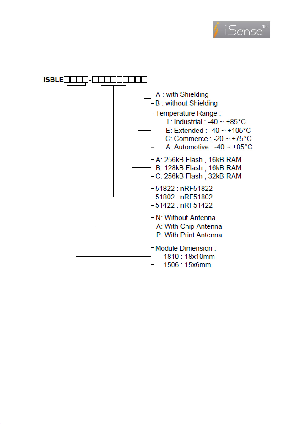
2. P/N Number Define
Figure 1 : P/N Number Define
5

3. Module Dimension
Unit : mm
3.1 Product Dimensions
ISBLE1810-P51xxxxxA
Figure 2 : Product Dimensions (ISBLE1810-P51xxxxxA)
ISBLE1506-A51xxxxxA
Figure 3 : Product Dimensions (ISBLE1506-A51xxxxxA)
6

3.2 Pin Descriptions
Pin NO.
Name
Pin function
Description
1
GND
Ground
The pad must be connected to a solid ground plane
2
GND
Ground
The pad must be connected to a solid ground plane
3
GND
Ground
The pad must be connected to a solid ground plane
4
P0.21
Digital I/O
General-purpose digital I/O
5
P0.22
Digital I/O
General-purpose digital I/O
6
P0.23
Digital I/O
General-purpose digital I/O
7
P0.24
Digital I/O
General-purpose digital I/O
8
P0.25
Digital I/O
General-purpose digital I/O
9
AVDD
Power
Analog power supply
10
P0.29
Digital I/O
General-purpose digital I/O
11
P0.28
Digital I/O
General-purpose digital I/O
12
DCC
Power
DC/DC output voltage to external LC filter
13
VDD_NRF
Power
Power supply
14
VDD_NRF
Power
Power supply
ISBLE1810-P51xxxxxA
Figure 4 : Module Pin Descriptions (ISBLE1810-P51xxxxxA)
7

Pin NO.
Name
Pin function
Description
15
GND
Ground
The pad must be connected to a solid ground plane
16
GND
Ground
The pad must be connected to a solid ground plane
17
P0.26
Digital I/O
General-purpose digital I/O
AIN0
Analog input
ADC input 2
XL2
Analog output
Connector for 32.768KHz crystal
18
P0.27
Digital I/O
General-purpose digital I/O
AIN1
Analog input
ADC input 2
XL1
Analog output
Connector for 32.768KHz crystal
19
P0.30
Digital I/O
General-purpose digital I/O
20
P0.00
Digital I/O
General-purpose digital I/O
AREF0
Analog input
ADC Reference voltage
21
P0.01
Digital I/O
General-purpose digital I/O
AIN2
Analog input
ADC input 2
22
P0.02
Digital I/O
General-purpose digital I/O
AIN3
Analog input
ADC input 3
23
P0.03
Digital I/O
General-purpose digital I/O
AIN4
Analog input
ADC input 4
24
P0.04
Digital I/O
General-purpose digital I/O
AIN5
Analog input
ADC input 5
25
P0.05
Digital I/O
General-purpose digital I/O
AIN6
Analog input
ADC input 6
26
P0.06
Digital I/O
General-purpose digital I/O
AIN7
Analog input
ADC input 7
AREF1
Analog input
ADC Reference voltage
27
P0.07
Digital I/O
General-purpose digital I/O
28
N.C.
/
/
29
GND
Ground
The pad must be connected to a solid ground plane
30
P0.08
Digital I/O
General-purpose digital I/O
31
P0.09
Digital I/O
General-purpose digital I/O
32
P0.10
Digital I/O
General-purpose digital I/O
33
P0.11
Digital I/O
General-purpose digital I/O
34
P0.12
Digital I/O
General-purpose digital I/O
35
P0.13
Digital I/O
General-purpose digital I/O
36
P0.14
Digital I/O
General-purpose digital I/O
37
P0.15
Digital I/O
General-purpose digital I/O
38
P0.16
Digital I/O
General-purpose digital I/O
8

Pin NO.
Name
Pin function
Description
39
P0.17
Digital I/O
General-purpose digital I/O
40
SWDIO
Digital I/O
Also HW debug and flash programming I/O
RESET
Digital I/O
System reset(active low).
41
SWDCLK
Digital input
HW debug and flash programming. Connect a 12K ohm
resister to GND for flash programming .
42
P0.18
Digital I/O
General-purpose digital I/O
43
P0.19
Digital I/O
General-purpose digital I/O
44
P0.20
Digital I/O
General-purpose digital I/O
45
GND
Ground
The pad must be connected to a solid ground plane
46
GND
Ground
The pad must be connected to a solid ground plane
1. Digital I/O pad with 5mA source/sink capability.
Table 1 : Pin function (ISBLE1810-P51xxxxxA)
ISBLE1506-A51xxxxxA
Figure 5 : Module Pin Descriptions (ISBLE1506-A51xxxxxA)
9
Pin NO.
Name
Pin function
Description
1
P0.18
Digital I/O
General-purpose digital I/O
2
P0.20
Digital I/O
General-purpose digital I/O
3
SWDCLK
Digital input
HW debug and flash programming. Connect a 12K ohm
resister to GND for flash programming .
4
SWDIO
Digital I/O
Also HW debug and flash programming I/O
RESET
Digital I/O
System reset(active low)
5
P0.17
Digital I/O
General-purpose digital I/O
6
P0.19
Digital I/O
General-purpose digital I/O
7
P0.16
Digital I/O
General-purpose digital I/O
8
P0.15
Digital I/O
General-purpose digital I/O
9
P0.12
Digital I/O
General-purpose digital I/O
10
P0.11
Digital I/O
General-purpose digital I/O
11
P0.09
Digital I/O
General-purpose digital I/O
12
P0.08
Digital I/O
General-purpose digital I/O
13
P0.14
Digital I/O
General-purpose digital I/O
14
P0.13
Digital I/O
General-purpose digital I/O
15
P0.10
Digital I/O
General-purpose digital I/O
16
GND
Ground
The pad must be connected to a solid ground plane
17
P0.07
Digital I/O
General-purpose digital I/O
18
P0.05
Digital I/O
General-purpose digital I/O
AIN6
Analog input
ADC input 6
19
P0.06
Digital I/O
General-purpose digital I/O
AIN7
Analog input
ADC input 7
AREF1
Analog input
ADC Reference voltage
20
P0.03
Digital I/O
General-purpose digital I/O
AIN4
Analog input
ADC input 4
21
P0.01
Digital I/O
General-purpose digital I/O
AIN2
Analog input
ADC input 2
22
P0.02
Digital I/O
General-purpose digital I/O
AIN3
Analog input
ADC input 3
23
P0.00
Digital I/O
General-purpose digital I/O
AREF0
Analog input
ADC Reference voltage
24
GND
Ground
The pad must be connected to a solid ground plane
25
DCC
Power
DC/DC output voltage to external LC filter
26
P0.04
Digital Input
General-purpose digital I/O
AIN5
Analog input
ADC input 5
10

Pin NO.
Name
Pin function
Description
27
P0.31
Digital I/O
General-purpose digital I/O
28
P0.30
Digital I/O
General-purpose digital I/O
29
VCC_nRF
Power
Power supply
30
AVDD
Power
Analog power supply
31
P0.29
Digital I/O
General-purpose digital I/O
32
P0.28
Digital I/O
General-purpose digital I/O
33
P0.27
Digital I/O
General-purpose digital I/O
AIN1
Analog input
ADC input 1
XL1
Analog input
Connector for 32.768KHz crystal
34
P0.26
Digital I/O
General-purpose digital I/O
AIN0
Analog input
ADC input 0
XL2
Analog output
Connector for 32.768KHz crystal
35
P0.24
Digital I/O
General-purpose digital I/O
36
P0.21
Digital I/O
General-purpose digital I/O
37
P0.22
Digital I/O
General-purpose digital I/O
38
P0.25
Digital I/O
General-purpose digital I/O
39
P0.23
Digital I/O
General-purpose digital I/O
40
RF
RFout
2.4GHz 50ohm RF out, not need to mount.
41
GND
Ground
The pad must be connected to a solid ground plane
42
GND
Ground
The pad must be connected to a solid ground plane
1. Digital I/O pad with 5mA source/sink capability.
Table 2 : Pin function (ISBLE1506-A51xxxxxA)
11

3.3 PCB Layout Guide
ISBLE1810-P51xxxxxA
Figure 6 : PCB Layout Guide (ISBLE1810-P51xxxxxA)
ISBLE1506-A51xxxxxA
Figure 7 : PCB Layout Guide (ISBLE1506-A51xxxxxA)
12
4. Main Chip Solution
RF IC
Crystal Frequency
Nordic nRF51822-QFAA
16MHz
Nordic nRF51822-CEAA
16MHz
Part Number
Package
ISBLE1810-P51822ACA
500 PCS/BOX
ISBLE1506-A51822ACA
500 PCS/BOX
Table 3 : Main Chip Solution
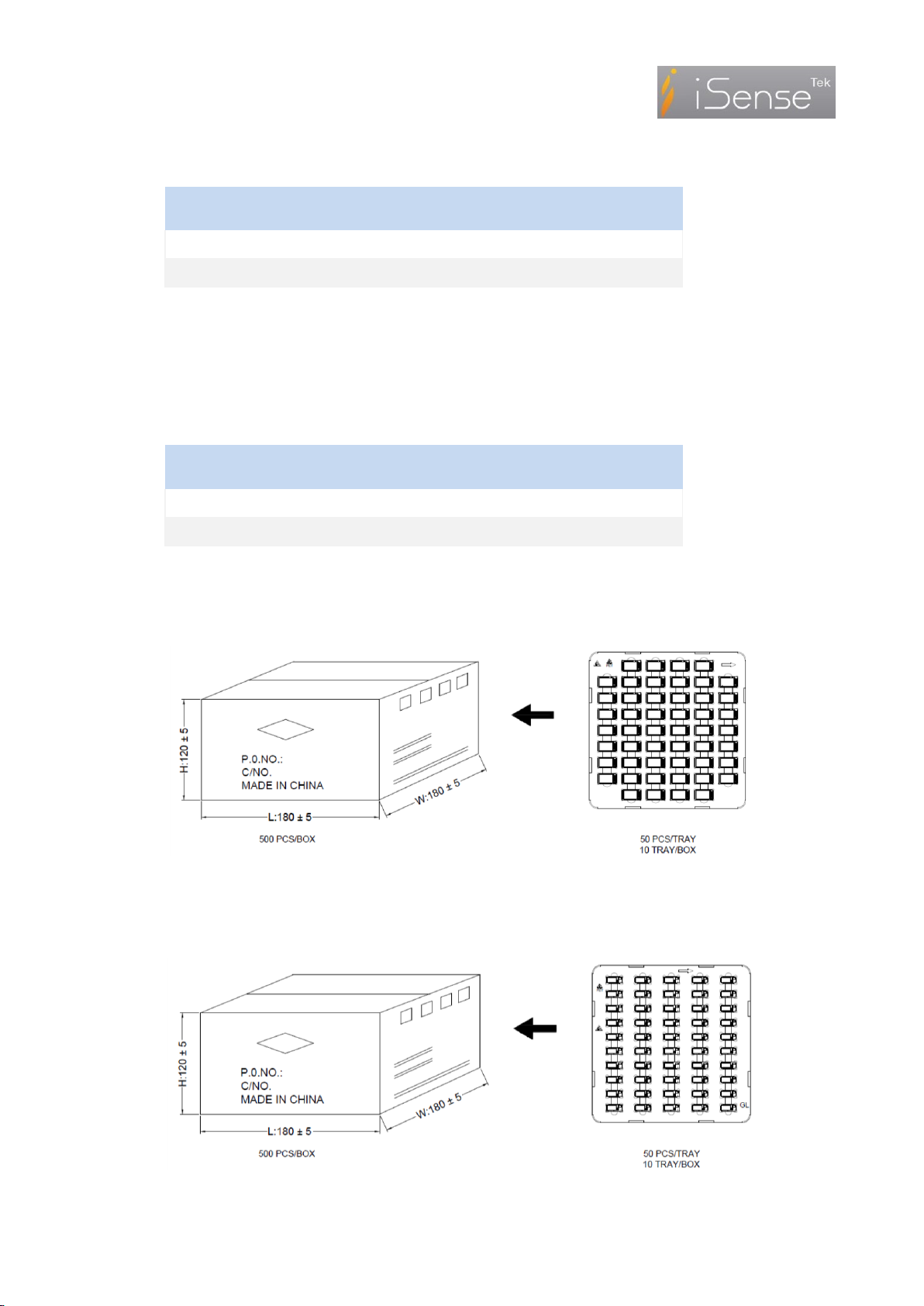
5. Shipment Packing Information
ISBLE1810-P51xxxxxA
Figure 8 : Packing Information (ISBLE1810-P51xxxxxA)
ISBLE1506-A51xxxxxA
Table 4 : Shipment Packing Information
Figure 9 : Packing Information (ISBLE1810-P51xxxxxA)
13
6. Specification
Symbol
Parameter
Min.
Max.
Units
Supply voltages
VDD -0.3
+3.9
V
DEC2 2 V
VSS 0 V
I/O pin voltage
VIO -0.3
VDD+0.3
V
Environmental QFN48 package
Storage temperature
-40
+125
°C
MSL
Moisture Sensitivity Level
2
ESD HBM
Human Body Model
3 kV
ESD CDM
Charged Device Model
750
V
Environmental WLCSP package
Storage temperature
-40
+125
°C
MSL
Moisture Sensitivity Level
1
ESD HBM
Human Body Model
4 kV
ESD CDM
Charged Device Model
500
V
Flash memory
Endurance
20000 1
Write /
erase cycles
Retention
10 years at 40 °C
50 years at 25 °C
Number of times an address
can be written between
erase cycles
2 times
6.1 Absolute Maximum Ratings
Maximum ratings are the extreme limits the chip can be exposed to without causing
permanent damage. Exposure to absolute maximum ratings for prolonged periods of time
may affect the reliability of the chip.
Table 5 specifies the absolute maximum ratings.
1. Flash endurance is 20,000 erase cycles. The smallest element of flash that can be written is a 32 bit word.
Table 5 : Absolute maximum ratings
14

6.2 Operation Conditions
Symbol
Parameter
Notes
Min.
Typ.
Max.
Units
VDD
Supply voltage, internal LDO setup
1.8
3.0
3.6
V
VDD
Supply voltage, DC/DC converter setup
2.1
3.0
3.6
V
VDD
Supply voltage, low voltage mode setup
1
1.75
1.8
1.95
V
t
R_VDD
Supply rise time (0 V to VDD)
2
100
ms
TA
Operating temperature
-25
25
75
°C
Symbol
Parameter
Notes
Min.
Typ.
Max.
Units
Test
Level
fOP
Operating frequencies.
1 MHz channel
spacing
2400
2483
MHz
N/A
PLL
res
PLL programming resolution.
1 MHz
N/A
Δf
250
Frequency deviation at 250 kbps.
±170
kHz
2
Δf1M
Frequency deviation at 1 Mbps.
±170
kHz
2
Δf2M
Frequency deviation at 2 Mbps.
±320
kHz
2
Δf
BLE
Frequency deviation at BLE.
±225
±250
±275
kHz
4
bps
FSK
On-air data rate.
250
2000
kbps
N/A
Symbol
Parameter
Notes
Min.
Typ.
Max.
Units
Test
Level
I
TX,+4dBm
TX only run current at P
OUT
= +4 dBm.
1
16 mA
4
I
TX,0dBm
TX only run current at P
OUT
= 0 dBm.
1
10.5 mA
4
I
TX,-4dBm
TX only run current at P
OUT
= -4 dBm.
1 8 mA
2
I
TX,-8dBm
TX only run current at P
OUT
= -8 dBm.
1 7 mA
2
The operating conditions are the physical parameters that the chip can operate within as
defined in Table 6.
1. DEC2 shall be connected to VDD in this mode.
2. The on-chip power-on reset circuitry may not function properly for rise times outside the specified interval.
Table 6 : Operating conditions
6.3 Electrical Specifications
6.3.1 Radio Transceiver
General radio characteristics
Table 7 : General radio characteristics
Radio current consumption
15

Symbol
Parameter
Notes
Min.
Typ.
Max.
Units
Test
Level
I
TX,-12dBm
TX only run current at P
OUT
= -12 dBm.
1
6.5 mA
2
I
TX,-16dBm
TX only run current at P
OUT
= -16 dBm.
1 6 mA
2
I
TX,-20dBm
TX only run current at P
OUT
= -20 dBm.
1
5.5 mA
2
I
TX,-30dBm
TX only run current at P
OUT
= -30 dBm.
1
5.5 mA
2
I
START,TX
TX startup current.
2 7 mA
1
I
RX,250
RX only run current at 250 kbps.
12.6 mA
1
I
RX,1M
RX only run current at 1 Mbps.
13 mA
4
I
RX,2M
RX only run current at 2 Mbps.
13.4 mA
1
I
START
RX startup current.
3
8.7 mA
1
Symbol
Description
Min.
Typ.
Max.
Units
Test
Level
PRF
Maximum output power.
4
dBm
4
P
RFC
RF power control range.
20
24 dB
2
P
RFCR
RF power accuracy.
±4
dB
1
P
WHISP
RF power whisper mode.
-30 dBm
2
P
BW2
20 dB bandwidth for modulated carrier (2 Mbps).
1800
2000
kHz
2
P
BW1
20 dB bandwidth for modulated carrier (1 Mbps).
950
1100
kHz
2
P
BW250
20 dB bandwidth for modulated carrier (250 kbps).
700
800
kHz
2
P
RF1.2
1st Adjacent Channel Transmit Power.
±2 MHz (2 Mbps).
-20
dBc
2
P
RF2.2
2nd Adjacent Channel Transmit Power.
±4 MHz (2 Mbps).
-45
dBc
2
P
RF1.1
1st Adjacent Channel Transmit Power.
±1 MHz (1 Mbps).
-20
dBc
2
P
RF2.1
2nd Adjacent Channel Transmit Power.
±2 MHz (1 Mbps).
-40
dBc
2
P
RF1.250
1st Adjacent Channel Transmit Power.
±1 MHz (250 kbps).
-25
dBc
2
P
RF2.250
2nd Adjacent Channel Transmit Power.
±2 MHz (250 kbps).
-40
dBc
2
1. Valid for data rates 250 kbps, 1 Mbps, and 2 Mbps.
2. Average current consumption (at 0 dBm TX output power) for TX startup (130 μs), and when changing mode from RX toTX (130 μs).
3. Average current consumption for RX startup (130 μs), and when changing mode from TX to RX (130 μs).
Table 8 : Radio current consumption
6.3.2 Transmitter Specifications
16

Symbol
Description
Min.
Typ.
Max.
Units
Test
Level
t
TX,30
Maximum consecutive transmission time,
f
TOL
< ±30 ppm.
16
ms
1
t
TX,60
Maximum consecutive transmission time,
f
TOL
< ±60 ppm.
4
ms
1
Symbol
Description
Min.
Typ.
Max.
Units
Test
Level
Receiver operation
PRX
MAX
Maximum received signal strength at < 0.1%
PER.
0
dBm
1
PRX
SENS,2M
Sensitivity (0.1% BER) at 2 Mbps.
-85 dBm
2
PRX
SENS,1M
Sensitivity (0.1% BER) at 1 Mbps.
-90 dBm
2
PRX
SENS,250k
Sensitivity (0.1% BER) at 250 kbps.
-96 dBm
2
P
SENS
IT
1 Mbps BLE
Receiver sensitivity: Ideal transmitter.
-93 dBm
2
P
SENS
DT
1 Mbps BLE
Receiver sensitivity: Dirty transmitter.1
-91 dBm
2
RX selectivity - modulated interfering signal
2
2 Mbps
C/ICO
C/I co-channel.
12 dB
2
C/I
1ST
1
st
ACS, C/I 2 MHz.
-4 dB
2
C/I
2ND
2nd ACS, C/I 4 MHz.
-24 dB
2
C/I
3RD
3rd ACS, C/I 6 MHz.
-28 dB
2
C/I
6th
6th ACS, C/I 12 MHz.
-44 dB
2
C/I
Nth
Nth ACS, C/I fi > 25 MHz.
-50 dB
2
1 Mbps
C/ICO
C/I co-channel (1 Mbps).
12 dB
2
C/I
1ST
1st ACS, C/I 1 MHz.
4
dB
2
C/I
2ND
2nd ACS, C/I 2 MHz.
-24 dB
2
C/I
3RD
3rd ACS, C/I 3 MHz.
-30 dB
2
C/I
6th
6th ACS, C/I 6 MHz.
-40 dB
2
C/I
12th
12th ACS, C/I 12 MHz.
-50 dB
2
C/I
Nth
Nth ACS, C/I fi > 25 MHz.
-53 dB
2
Table 9 : Transmitter specifications
6.3.3 Receiver Specifications
17

Symbol
Description
Min.
Typ.
Max.
Units
Test
Level
250 kbps
C/ICO
C/I co-channel.
4
dB
2
C/I
1ST
1st ACS, C/I 1 MHz.
-10 dB
2
C/I
2ND
2nd ACS, C/I 2 MHz.
-34 dB
2
C/I
3RD
3rd ACS, C/I 3 MHz.
-39 dB
2
C/I
6th
6th ACS, C/I fi > 6 MHz.
-50 dB
2
C/I
12th
12th ACS, C/I 12 MHz.
-55 dB
2
C/I
Nth
Nth ACS, C/I fi > 25 MHz.
-60 dB
2
Bluetooth Low Energy RX selectivity
C/ICO
C/I co-channel.
10 dB
2
C/I
1ST
1st ACS, C/I 1 MHz.
1
dB
2
C/I
2ND
2nd ACS, C/I 2 MHz.
-25 dB
2
C/I3+N
ACS, C/I (3+n) MHz offset [n = 0, 1, 2, . . .].
-51 dB
2
C/IImage
lmage blocking level.
-30 dB
2
C/IImage±1MHz
Adjacent channel to image blocking level
(±1 MHz).
-31 dB
2
RX intermodulation
3
P_IMD
2Mbps
IMD performance, 2 Mbps,
3rd, 4th, and 5th offset channel.
-41 dBm
2
P_IMD
1Mbps
IMD performance, 1 Mbps,
3rd, 4th, and 5th offset channel.
-40 dBm
2
P_IMD
250kbps
IMD performance, 250 kbps,
3rd, 4th, and 5th offset channel.
-36 dBm
2
P_IMD
BLE
IMD performance, 1 Mbps BLE,
3rd, 4th, and 5th offset channel.
-39 dBm
2
1. As defined in the Bluetooth Core Specification v4.0 Volume 6: Core System Package (Low Energy Controller Volume).
2. Wanted signal level at PIN = -67 dBm. One interferer is used, having equal modulation as the wanted signal. The input power of the
interferer where the sensitivity equals BER = 0.1% is presented.
3. Wanted signal level at PIN = -64 dBm. Two interferers with equal input power are used. The interferer closest in fre-quency is not
modulated, the other interferer is modulated equal with the wanted signal. The input power of interferers where the s ensitivity
equals BER = 0.1% is presented.
Table 10 : Receiver specifications
18

6.3.4 Radio Timing Parameters
Symbol
Description
250 k
1 M
2 M
BLE
Jitter
Units
t
TXEN
Time between TXEN task and
READY event.
132
132
132
140 0 μs
t
TXDISABLE
Time between DISABLE task
and DISABLED event when the
radio was in TX.
10 4 3 4 1
μs
t
RXEN
Time between the RXEN task
and READY event.
130
130
130
138 0 μs
t
RXDISABLE
Time between DISABLE task
and DISABLED event when the
radio was in RX.
0 0 0 0 1
μs
t
TXCHAIN
TX chain delay.
5 1 0.5 1 0
μs
t
RXCHAIN
RX chain delay.
12.5 3 2 3 0
μs
Symbol
Description
Notes
Min.
Typ.
Max.
Units
Test
Level
RSSI
ACC
RSSI accuracy.
Valid range
-50 dBm to -80 dBm.
±6
dB
2
RSSI
RESOLUTION
RSSI resolution.
1
dB
1
RSSI
PERIOD
Sample period.
8.8
μs
1
RSSI
CURRENT
Current consumption in
addition to IRX.
250 μA
1
Symbol
Description
Min.
Typ.
Max.
Units
Test
Level
I
CPU, FLASH
Run current at 16 MHz (XOSC). Executing
code from flash memory.
4.1 mA
2
I
CPU, RAM
Run current at 16 MHz (XOSC). Executing
code from RAM.
2.4 mA
1
I
START, CPU
CPU startup current.
600 μA
1
t
START, CPU
IDLE to CPU execute.
0
μs
1
6.3.5 RSSI Specifications
Table 12 : RSSI specifications
6.3.6 CPU
Table 11 : Radio timing
Table 13 : RSSI specifications
19

6.3.7 Power Management
Symbol
Description
Min.
Typ.
Max.
Units
Test
Level
I
OFF
Current in SYSTEM OFF, no RAM retention.
0.6 1 μA
2
I
OFF, RET, 8k
Additional current in SYSTEM OFF per
retained RAM block (8 kB).
0.6 1 μA
2
I
OFF2ON
OFF to CPU execute transition current.
400 μA
1
t
OFF2ON
OFF to CPU execute.
9.6
10.6
μs
1
I
ON,16k
SYSTEM-ON base current with 16 kB RAM
enabled.
2.6 1 μA
2
I
ON,32k
SYSTEM-ON base current with 32 kB RAM
enabled.
3.8 1 μA
2
t
1V2
Startup time for 1V2 regulator.
2.3 μs
1
I
1V2XO16
Current drawn by 1V2 regulator and 16 MHz
XOSC when both are on at the same time.
810 2
μA
1
I
1V2XO32
Current drawn by 1V2 regulator and 32 MHz
XOSC when both are on at the same time.
840 2
μA
1
I
1V2RC16
Current drawn by 1V2 regulator and 16 MHz
RCOSC when both are on at the same time.
880 2
μA
1
I
1V2XO16,1M
For HFCLK in 1 MHz mode3. Current drawn
by 1V2 regulator and 16 MHz XOSC when
both are on at the same time.
520 2
μA
1
I
1V2XO32,1M
For HFCLK in 1 MHz mode3. Current drawn
by 1V2 regulator and 32 MHz XOSC when
both are on at the same time.
560 2
μA
1
I
1V2RC16,1M
For HFCLK in 1 MHz mode3. Current drawn
by 1V2 regulator and 16 MHz RCOSC when
both are on at the same time.
630 2
μA
1
tXO
Startup time for the clock management
system when the XTAL is in standby.
2.3 μs
1
t
1V7
Startup time for 1V7 regulator.
2 3.6
μs
1
I
1V7
Current drawn by 1V7 regulator.
105 μA
2
F
DCDC
DC/DC converter current conversion factor.
0.65 4
1.2 4 1
1. Add 1 μA to the current value if the device is used in Low voltage mode.
2. This number includes the current used by the automated power and clock management system.
3. For details on 1 MHz mode, see Section 4.2 “Timer/counters (TIMER)” on page 33.
4. FDCDC will vary depending on VDD and internal radio current consumption (IDD). Please refer to the nRF51 Series Refer-ence
Manual, v3.0 or later, for a method to calculate IDD,DCDC. See Figure 11 on page 51 for a DC/DC conversion factor chart.
Table 14 : Power management
20

7. Reference Circuit
7.1 Schematic with Internal LDO
Figure 10 : Schematic with internal LDO
21

7.2 Schematic with Internal DC/DC Converter
Figure 11 : Schematic with internal DC/DC converter
22

8. Development Kit
Support USB to UART for DTM use
Button *4 and LED *4
32 Pin GPIO to 2.54mm Female Pin Holder
Support Module Test Socket
Development Kit for ISBLE1810
Figure 12 : Development Kit for ISBLE1810
23

Development Kit for ISBLE1506
Support USB to UART for DTM use
Button *4 and LED *4
32 Pin GPIO to 2.54mm Female Pin Holder
Support Module Test Socket
Figure 13 : Development Kit for ISBLE1506
24

9. Antenna Forbidden Zone Description
Material \ Dimension
A B C
D
FR4 (without Copper)
≧ 1mm
≧ 3mm
≧ 1mm
≧ 3mm
FR4 (with Copper)
≧ 4mm
≧ 7mm
≧ 10mm
≧ 4mm
Metal
≧ 4mm
≧ 3.5mm
≧ 10mm
≧ 3mm
Plastic
≧ 1mm
≧ 1mm
≧ 1mm
≧ 3mm
The PCB and mechanism design need to meet antenna forbidden zone description Table.
Otherwise affect the efficiency of the antenna.
ISBLE1810-P51xxxxxA
Figure 14 : Antenna Forbidden Zone Description (ISBLE1810-P51xxxxxA)
Table 15 : Antenna Forbidden Zone List (ISBLE1810-P51xxxxxA)
25

ISBLE1506-A51xxxxxA
Material \ Dimension
A B C
D
FR4 (without Copper)
≧ 2mm
≧ 3mm
≧ 0.5mm
≧ 5mm
FR4 (with Copper)
≧ 6mm
≧ 6mm
≧ 3mm
≧ 8mm
Metal
≧ 6mm
≧ 6mm
≧ 3mm
≧ 8mm
Plastic
≧ 2mm
≧ 2mm
≧ 0.5mm
≧ 3.5mm
Figure 15 : Antenna Forbidden Zone Description (ISBLE1506-P51xxxxxA)
Table 16 : Antenna Forbidden Zone List (ISBLE1506-P51xxxxxA)
26

10. Statements
Federal Communications Commission (FCC) Statement
15.21
You are cautioned that changes or modifications not expressly approved by the part
responsible for compliance could void the user’s authority to operate the equipment.
15.105(b)
This equipment has been tested and found to comply with the limits for a Class B digital
device, pursuant to part 15 of the FCC rules. These limits are designed to provide
reasonable protection against harmful interference in a residential installation. This
equipment generates, uses and can radiate radio frequency energy and, if not installed and
used in accordance with the instructions, may cause harmful interference to radio
communications. However, there is no guarantee that interference will not occur in a
particular installation. If this equipment does cause harmful interference to radio or
television reception, which can be determined by turning the equipment off and on, the user
is encouraged to try to correct the interference by one or more of the following measures:
- Reorient or relocate the receiving antenna.
- Increase the separation between the equipment and receiver.
- Connect the equipment into an outlet on a circuit different from that to which the
receiver is connected.
- Consult the dealer or an experienced radio/TV technician for help.
This device complies with Part 15 of the FCC Rules. Operation is subject to the following
two conditions:
1) this device may not cause harmful interference, and
2) this device must accept any interference received, including interference that may cause
undesired operation of the device.
FCC RF Radiation Exposure Statement :
This equipment complies with FCC radiation exposure limits set forth for an uncontrolled
environment. End users must follow the specific operating instructions for satisfying RF
exposure compliance. This transmitter must not be co-located or operating in conjunction
with any other antenna or transmitter.
Note: The end product shall have the words “Contains Transmitter Module FCC ID:
2AI2V-ISBLE1810X5 “
27

11. Document History
Revision
Date
Description/Changes
1.0
2014/01/22
First Release
1.1
2014/09/18
Update EVB information
2.0
2016/04/25
New Approval Sheet
2.1
2016/07/14
1. Modify ISBLE1506-A51xxxxxA capacitive C8、C9 position.
2. Update P/N Number Define. P5
3. ISBLE1506-A51xxxxxA & ISBLE1810-P51xxxxxA add shielding
Marking and test point for PCB Bottom layer. P6
4. Update PCB layout guide information. P12
5. Update development kit information & Photos. P23、24
6. Add RF Exposure Warning Statement. P28
28
 Loading...