

Page 1
Spezialelektronik GmbH
iseg Spezialelektronik GmbH Email: sales@iseg-hv.de Phone ++ 49 351 / 26 996 - 0
Bautzner Landstr. 23 http://www.iseg-hv.com Fax ++ 49 351 / 26 996 - 21
D - 01454 Radeberg / Rossendorf Germany
Precision High Voltage Supply VME STANDARD series
Operators Manual
Contents:
1. General information
2. Technical Data
3. VHQ Description
4. Front panel
5. Handling
6. VME Interface
7. Program example
Appendix A: Block diagram
Appendix B: Rotary switch locations
Attention!
-It is not allowed to use the unit if the covers have been
removed.
-We decline all responsibility for damages and injuries
caused by an improper use of the module. It is highly
recommended to read the operators manual before any
kind of operation.
Note
The information in this manual is subject to change without notice. We take no responsibility whatsoever for any
error in the document. We reserve the right to make changes in the product design without reservation and
without notification to the users.
Filename VHQx0x.___; version 3.00 as of 24.09.2004
Page 2
Spezialelektronik GmbH
iseg Spezialelektronik GmbH Email: sales@iseg-hv.de Phone ++ 49 351 / 26 996 - 0
Bautzner Landstr. 23 http://www.iseg-hv.com Fax ++ 49 351 / 26 996 - 21
D - 01454 Radeberg / Rossendorf Germany 2
1. General information
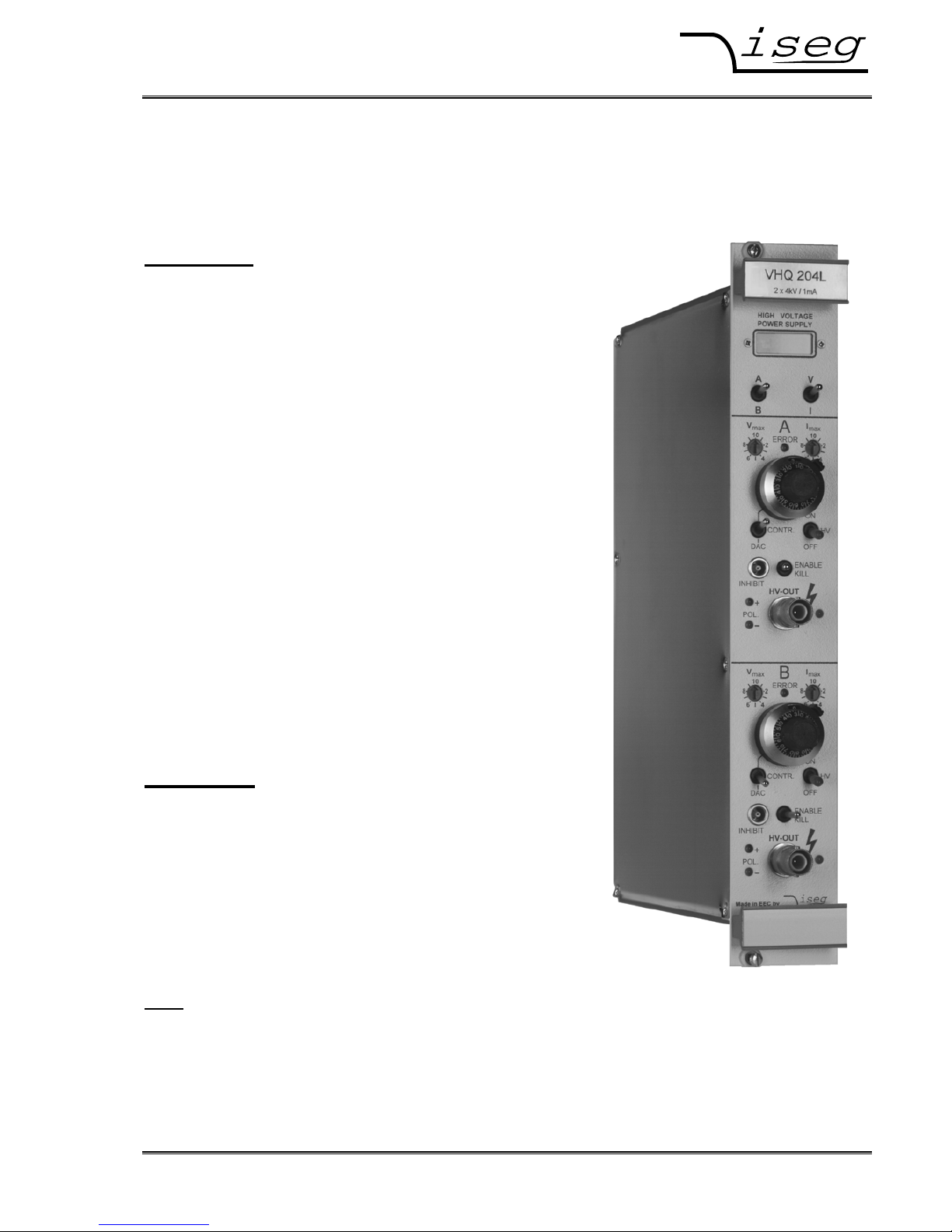
The VHQ´s are two channel high voltage supplies in 6U VME format, 164 mm deep, double width. The units
offers manual control and operation via VME bus. The use of the VME interface supports more then the manual
control functionality.
The high voltage supplies special provide high precision output voltage together with very low ripple and noise,
even under full load. Separate 10%-steps hardware switches put voltage and current limits. An INHIBIT input
protects connected sensitive devices. Additionally, the maximal output current per channel is programmable via
the interface. The high voltage outputs protected against overload and short circuit. The output polarity can be
switched over. The HV-GND is connected to the chassis and the powering GND.
2. Technical data:
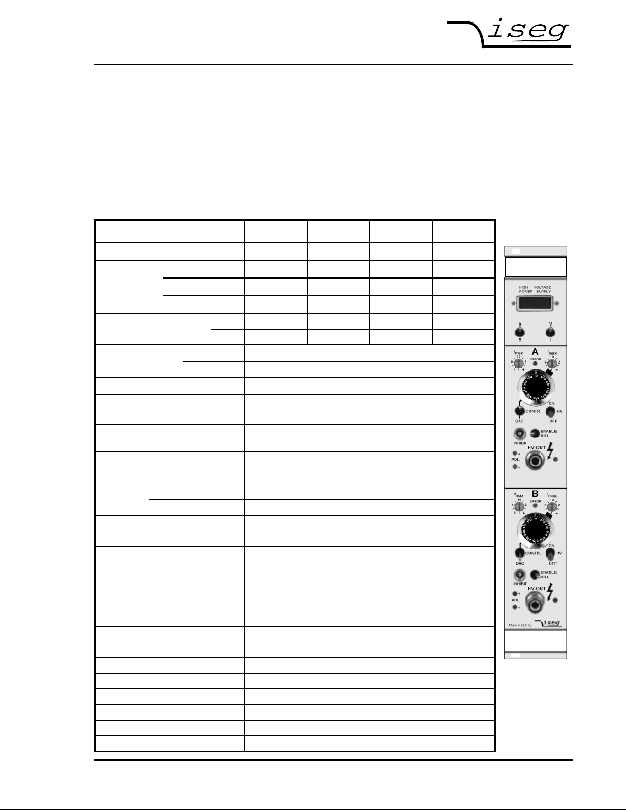
VHQ two channel 202 M 203 M 204 L 205 L
Output voltage V
O
0 ... 2 kV 0 ... 3 kV 0 ... 4 kV 0 ... 5 kV
Output current per channel I
O
0 ... 3 mA 0 ... 2 mA 0 ... 1 mA 0 ... 1 mA
with option M - h
0 ... 6 mA 0 ... 4 mA 0 ... 3 mA 0 ... 2 mA
with option _104
100 µA 100 µA 100 µA 100 µA
Ripple typ. < 0,5 mV
P-P
< 0,5 mV
P-P
< 1 mV
P-P
< 2 mV
P-P
max. 2 mV
P-P
2 mV
P-P
2 mV
P-P
5 mV
P-P
Stability
∆V
O
<5 ∗ 10
-5
(idle to max. load)
∆V
O
/∆V
INPUT
<5 ∗ 10
-5
Temperature coefficient
<5 ∗ 10
-5
/K
LCD Display 4 digits with sign, switch controlled
voltage display in [V] / current display in [µA]
Resolution of measurement
Current: 1 µA, with option _104: 100 nA
Voltage: 1 V
Accuracy current measurement
±(0,05% I
O
+ 0,02% I
O max
+ 1 digit) (for one year)
Accuracy voltage measurement
±(0,05% V
O
+ 0,02% V
O max
+ 1 digit) (for one year)
Voltage CONTROL switch in upper position: 10 - turn potentiometer
control lower position (DAC): control via interface
Rate of change of hardware ramp 500 V/s (on HV-ON/ -OFF)
output voltage software ramp: 2 . . . 255 V/s
Protection - separate current and voltage limit
(hardware, rotary switch in 10%-steps)
- INHIBIT (ext. signal TTL-level,
Low = active ⇒ V
OUT
=0)
- programmable current limit (software)
Current trip reaction time < 60 ms
Power requirements V
INPUT
± 12 V ( < 850 mA, with option M - h < 1,6 A)
+ 5 V ( < 300 mA)
Packing VME #2 / 6U / 164 mm deep
Connector 96-pin VME connector according to DIN 41612
HV connector SHV-Connector at the front panel
INHIBIT connector 1-pin Lemo-hub
Operating temperature 0 ... +50 °C
Storage temperature -20 ... +60 °C
VHQ 205L
2 x 5 kV / 1 mA
Page 3
Spezialelektronik GmbH
iseg Spezialelektronik GmbH Email: sales@iseg-hv.de Phone ++ 49 351 / 26 996 - 0
Bautzner Landstr. 23 http://www.iseg-hv.com Fax ++ 49 351 / 26 996 - 21
D - 01454 Radeberg / Rossendorf Germany 3
3. VHQ Description
The function is described at a block diagram of the VHQ. This can be found in Appendix A.
High voltage supply
A patented high efficiency resonance converter circuit, which provides a low harmonic sine voltage on the HVtransformer, is used to generate the high voltage. The high voltage is rectified using a high speed HV-rectifier,
and the polarity is selected via a high-voltage switch. A consecutive active HV-filter damps the residual ripple
and ensures low ripple and noise values as well as the stability of the output voltage. A precision voltage divider
is integrated into the HV-filter to provide the set value of the output voltage, an additional voltage divider
supplies the measuring signal for the maximum voltage control. A precision measuring and AGC amplifier
compares the actual output voltage with the set value given by the DAC (computer control) or the potentiometer
(manual control). Signals for the control of the resonance converter and the stabilizer circuit are derived from
the result of the comparison. The two-stage layout of the control circuit results in an output voltage, stabilized
with very high precision to the set point.
Separate security circuits prevent exceeding the front-panel switch settings for the current I
max
and voltage V
max
limits. A monitoring circuit prevents malfunction caused by low supply voltage.
The internal error detection logic evaluates the corresponding error signals and the external INHIBIT signal. It
allows the detection of short overcurrent due to single flashovers in addition.
Digital control unit
A micro controller handles the internal control, evaluation and calibration functions of both channels. The actual
voltages and currents are read cyclically by an ADC with connected multiplexer and processed for display on
the 4 digit LCD display. The current and voltage hardware limits are retrieved cyclically several times per
second. The reference voltage source provides a precise voltage reference for the ADC and generation of the
control signals in the manual operation mode of the unit.
The set values for the corresponding channels are generated by a 16-Bit DAC in computer controlled mode.
Filter
A special property of the unit is a tuned filtering concept, which prevents radiation of electromagnetic
interference into the unit, as well as the emittance of interference by the module. A filtering network is located
next to the connectors for the supply voltage and the converter circuits of the individual devices are also
protected by filters. The high-voltage filters are housed in individual metal enclosures to shield even minimum
interference radiation.
Page 4
Spezialelektronik GmbH
iseg Spezialelektronik GmbH Email: sales@iseg-hv.de Phone ++ 49 351 / 26 996 - 0
Bautzner Landstr. 23 http://www.iseg-hv.com Fax ++ 49 351 / 26 996 - 21
D - 01454 Radeberg / Rossendorf Germany 4
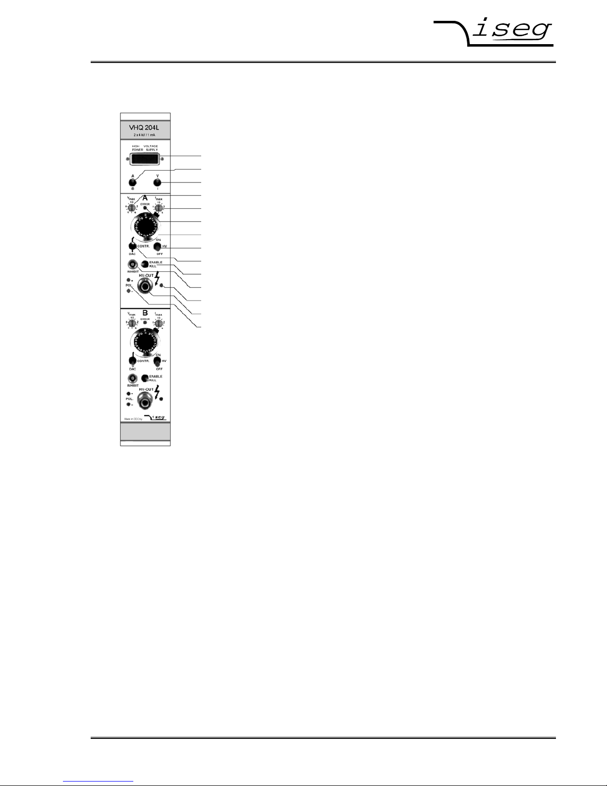
4. Front panel
[1] 4 digit LCD display
[2] Channel switch
[3] Measuring switch
[4] Rotary switch Voltage limit
[5] Rotary switch Current limit
[6] Error indicator
[7] 10 - turn potentiometer
[8] HV-ON switch
[9] CONTROL switch
[10] KILL switch
[11] INHIBIT input
[12] HV-ON indicator
[13] HV-output
[14] Polarity indicator
5. Handling
The state of readiness of the unit is produced at the VME connector on the flipside.
The Output polarity is selectable with help of a rotary switch on the cover side (see appendix B). The chosen
polarity is displayed by a LED on the front panel [14] and a sign on the LCD display [1].
Attention!
It is not allowed to change the polarity under power!
An undefined switch setting (not at one of the end positions) will cause no output voltage.
High voltage output is switched on with HV-ON switch [8] at the front panel. The viability is signaled by the
yellow LED [12].
Attention!
If the CONTROL switch [9] is in upper position (manual control), high voltage is generated
at HV-output [13] on the front panel with a ramp speed from 500 V/s (hardware ramp) to
the set voltage chosen via 10-turn potentiometer [7].
This is also the case, if VME control is switched over to manual control while operating.
If the CONTROL switch [9] is in lower position (DAC), high voltage will be activated only after receiving
corresponding VME commands.
Page 5

Spezialelektronik GmbH
iseg Spezialelektronik GmbH Email: sales@iseg-hv.de Phone ++ 49 351 / 26 996 - 0
Bautzner Landstr. 23 http://www.iseg-hv.com Fax ++ 49 351 / 26 996 - 21
D - 01454 Radeberg / Rossendorf Germany 5
On the LCD [1] output voltage in [V] or output current in [µA] will be displayed depending on the position of the
Measuring switch [3].
For the two channel units, one can choose with Channel switch [2], if channel (A) or channel (B) is displayed.
If working with manual control, output voltage can be set via 10-turn potentiometer [7] in a range from 0 to the
set maximal voltage.
If the CONTROL switch [9] is switched over to VME control, the DAC takes over the last set output voltage of
manual control. Output voltage can be generated with a programmable ramp speed (software ramp) from 2 to
255 V/s in a range from 0 to the maximal set voltage via VME control.
The maximum output current per channel can be set with a programmable current trip via the interface with the
resolution of current measurement. If the output current exceeds the programmable limit, the output voltage will
be shut off permanently by the software. Restoring the voltage is possible after reading ” Status register 2” and
then ”Start voltage change” via interface.
Maximum output voltage and current can be selected in 10%-steps with the rotary switches V
max
[4] and I
max
[5]
(switch dialed to 10 corresponds to 100%) independently of programmable current trip. The output voltage or
current, which exceed the limits, is signaled by the red error LED on the front panel [6].
Function of KILL switch [10]:
Switch to the right position:
(ENABLE KILL)
The output voltage will be shut off permanently without ramp on exceeding V
max
,
I
max
or in the presence of an INHIBIT signal (Low=active) at the INHIBIT input
[11]. Restoring the output voltage is possible after operating the switches HV-ON
or KILL or reading ” Status register 2” and then ”Start voltage change” by DAC
control.
Note: When capacitance is effective at the HV-output or when the rate of change of
output voltage is high (hardware ramp) at high load, then the KILL function will be
released by the current charging the condenser. In this case use a small rate of
output change (software ramp) or select ENABLE KILL not until output voltage is
set voltage.
Switch to the left position:
(DISABLE KILL)
The output voltage will be limited to V
max
, output current to I
max
respectively;
INHIBIT shuts the output voltage off without ramp, the previous voltage setting
will be restored with hard- or software ramp on INHIBIT no longer being present.
6. VME Interface
Modus: short supervisory access (AM = 0x2D)
short nonprivileged access (AM = 0x29)
Control via VME interface
1
st
write: set voltage, ramp speed, maximal output current (current trip)
2
nd
switch: output voltage = set voltage ; output voltage = 0
3
rd
read: set voltage; actual voltage; ramp speed; actual current; current trip
current and voltage hardware limit; status
Front panel switches are having priority over software control.
Manual control
While the unit is operated in manual control mode, VME read cycles are interpreted only. Commands are
accepted, but do not result in a change of the output voltage.
Page 6

Spezialelektronik GmbH
iseg Spezialelektronik GmbH Email: sales@iseg-hv.de Phone ++ 49 351 / 26 996 - 0
Bautzner Landstr. 23 http://www.iseg-hv.com Fax ++ 49 351 / 26 996 - 21
D - 01454 Radeberg / Rossendorf Germany 6
Command Execution Time
The command execution time is 2 µs typical.
Base Address
The base address BA is saved in a EEPROM. Setting BA:
1. Set both channels of the unit before power requirements (± 12V; + 5V) are activated as follows:
=> CONTROL switch at MANUELL; => HV-ON switch at OFF; => KILL switch at ENABLE.
2. Activate power requirements.
3. LCD display shows ”A” on the left side and the highbyte of the base address (e.g. ”dd”) on the right side,
with separator flashing in between.
4. High-order nibble can be set with channel switch and low-order nibble with measuring switch.
5. In case of no change for 10 s or of setting another switch respectively, the chosen base address is saved in
EEPROM and the unit is responsive with it.
6. Factory setting: BA = 0xDD00
Register addresses
The description for Channel B will be cancelled at the one channel unit.
A7 A6 A5 A4 A3 A2 A1 Read Write
0 0 0 0 0 0 0
Status register 1
0 0 0 0 0 1 0
Set voltage Channel A [V]
Set voltage Channel A (V
set
≤ V
max
) [V]
0 0 0 0 1 0 0
Set voltage Channel B [V]
Set voltage Channel B (V
set
≤ V
max
) [V]
0 0 0 0 1 1 0
Ramp speed Channel A (2... 255) [V/s] Ramp speed Channel A (2... 255) [V/s]
0 0 0 1 0 0 0
Ramp speed Channel B (2... 255) [V/s] Ramp speed Channel B (2... 255) [V/s]
0 0 0 1 0 1 0
Actual voltage Channel A [V]
0 0 0 1 1 0 0
Actual voltage Channel B [V]
0 0 0 1 1 1 0
Actual current Channel A
*
)
0 0 1 0 0 0 0
Actual current Channel B
*
)
0 0 1 0 0 1 0
Hardware limits Channel A (I
max
, V
max
)
0 0 1 0 1 0 0
Hardware limits Channel B (I
max
, V
max
)
0 0 1 0 1 1 0
Data ready
0 0 1 1 0 0 0
Status register 2
0 0 1 1 0 1 0
Start voltage change Channel A Start voltage change Channel A
with data: Set voltage Channel A [V]
0 0 1 1 1 0 0
Start voltage change Channel B Start voltage change Channel B
with data: Set voltage Channel B [V]
0 0 1 1 1 1 0
Module identifier
0 1 0 0 0 0 0
- -
0 1 0 0 0 1 0
Current software limit Channel A Current software limit Channel A
0 1 0 0 1 0 0
Current software limit Channel B Current software limit Channel B
*
) corresponding current resolution with data: maximal current Channel A/B
corresponding current resolution,
maximal current = 0 ⇒ not a current trip
Page 7

Spezialelektronik GmbH
iseg Spezialelektronik GmbH Email: sales@iseg-hv.de Phone ++ 49 351 / 26 996 - 0
Bautzner Landstr. 23 http://www.iseg-hv.com Fax ++ 49 351 / 26 996 - 21
D - 01454 Radeberg / Rossendorf Germany 7
Status register 1 (BA + 0x00)
Channel Bit Name Description 0 1
D15 ERROR_2 Error on Channel B Channel ok Error
D14 STATV_2 Status V
Out
V
out
stable V
out
in change
D13 TRENDV_2 Ramp up / down V
out
falling V
out
rising
B
D12 KILL_2 KILL switch setting Disabled Enabled
D11 ON_OFF_2 HV-ON/OFF switch setting On Off
D10 POL_2 Polarity V
Out
Negative Positive
D9 IN_EX_2 CONTROL switch setting DAC Manual
D8 VZ_2
V
Out
= 0
V
out
<>0 V
out
=0
D7 ERROR_1 Error on Channel A Channel ok Error
D6 STATV_1 Status V
Out
V
out
stable V
out
in change
D5 TRENDV_1 Ramp up / down V
out
falling V
out
rising
A
D4 KILL_1 KILL switch setting Disabled Enabled
D3 ON_OFF_1 HV-ON/OFF switch setting On Off
D2 POL_1 Polarity V
Out
Negative Positive
D1 IN_EX_1 CONTROL switch setting DAC Manual
D0 VZ_1
V
Out
= 0
V
out
<>0 V
out
=0
This register is representing the general status of the VHQ.
”Error“ is formed by the logic or of REG2ER_, REG1ER_, EXTINH_, RANGE_ and ILIM_
from ”Status register 2”.
”V
out
=0” is formed by DAC output = 0 and actual voltage < 5 V.
Set voltage Channel A/B (BA + 0x04 / BA + 0x08)
Set voltage V
set
from 0 to V
max
in V. If V
set
greater then V
max
(BA + 0x24 / BA + 0x28), V
set
will be not changed.
Ramp speed Channel A/B (BA + 0x0C / BA + 0x10)
Voltage ramp speed from 2 V/s to 255 V/s. All processor controlled changes in the output voltage are performed
at this ramp speed.
Actual voltage Channel A/B (BA + 0x14 / BA + 0x18)
Output voltage V
out’
of the channels in V.
Actual current Channel A/B (BA + 0x1C / BA + 0x20)
Output current I
out
of the channels corresponding current resolution.
Hardware limits (BA + 0x24 / BA + 0x28)
D0 .. D3 Maximal output current (I
max
) in 10 %, hardware setting on the front panel switches
D4 .. D7 Maximal output voltage (V
max
) in 10 %, hardware setting on the front panel switches
D8 .. D15 0
Data ready (BA + 0x2C)
D7 D6 D5 D4 D3 D2 D1 D0
0 0 0 0 Current B Voltage B Current A Voltage A
The individual bits are set as soon as actual measured data is existing. The bits are reset after the
corresponding reading command.
Page 8

Spezialelektronik GmbH
iseg Spezialelektronik GmbH Email: sales@iseg-hv.de Phone ++ 49 351 / 26 996 - 0
Bautzner Landstr. 23 http://www.iseg-hv.com Fax ++ 49 351 / 26 996 - 21
D - 01454 Radeberg / Rossendorf Germany 8
Status register 2 (BA + 0x30)
Bit Name Description Remark
D15 REG2ER_2 Quality of output voltage not given at present
D14 REG1ER_2 V
max
or I
max
is / was exceeded
Channel
D13 EXTINH_2 External inhibit was / is active
D12 RANGE_2 V
set
to V
max
ratio > 1 D(BA+0x08) > V
max
B
D11 KEY_CHANGED A frontpanel switch position was changed ON_OFF_2,
IN_EXT_2, KILL_2
D10 EOP_2 V
out
has reached set value End of process_2
D9 ILIM_2 I
out
was > I
max
programmable Current trip
D8
D7 REG2ER_1 Quality of output voltage not given at present
D6 REG1ER_1 V
max
or I
max
is / was exceeded
Channel
D5 EXTINH_1 External inhibit was / is active
D4 RANGE_1 V
set
to V
max
ratio > 1 A(BA+0x04) > V
max
A
D3 KEY_CHANGED A frontpanel switch position was changed ON_OFF_1,
IN_EXT_1, KILL_1
D2 EOP_1 V
out
has reached set value End of process_1
D1 ILIM_1 I
out
was > I
max
programmable Current trip
D0 TOT Timeout error New initialisation
The individual bits are set on the occurrence of the event. A general clear is performed after readout.
If the Output voltage was permanently switched off by exceeding V
max
or I
max
(ENABLE KILL resp. Current trip),
or INHIBIT respectively, the error bits (REG1ER_, EXTINH_, ILIM_) have to be reset by reading ” Status
register 2” before an output voltage can be set again.
Start voltage change (BA + 0x34 / Ba + 0x38)
A change in the output voltage of set voltage (BA + 0x04 / BA + 0x08) is performed by reading these registers.
Writing to the registers stores the data as new set voltage (V
set
≤ V
max
) and starts the voltage change.
The change of output voltage is blocked, if the conditions are unavailable to start voltage change corresponding
these description.
Command execution can be checked by reading status register 1 (BA + 0x00). The bits D14 (channel B), D6
(channel A) respectively are set on start of voltage change. Actual voltage reaching the set voltage is flagged by
the bits D10, D2 of status register 2 (BA + 0x30) respectively. An interruption of the voltage change (e.g.
external INHIBIT is active) is also ascertainable.
Module identifier (BA + 0x3C)
D15 .. D0 4 digit serial number, BCD coded
Current software limit (BA + 0x44 / BA + 0x48)
The maximal output current per channel corresponding current resolution. If the output current exceeds the
programmable limit, the output voltage will be shut off permanently by the software (Current trip). The Current
trip reaction time is lessen to 60 ms.
Writing to the registers with maximal output current = 0, not a current trip will be programmed.
Hardware maximum output current limit (I
max
) worked independently of programmable current software limit.
Page 9

Spezialelektronik GmbH
iseg Spezialelektronik GmbH Email: sales@iseg-hv.de Phone ++ 49 351 / 26 996 - 0
Bautzner Landstr. 23 http://www.iseg-hv.com Fax ++ 49 351 / 26 996 - 21
D - 01454 Radeberg / Rossendorf Germany 9
7. Program example
/**********************************************************************************/
/* vhq.c */
/* example program for iseg vme hv boards */
/* mki, 24.1.96 */
/* this code was compiled and run on an E6 under OS9 */
/* please contact iseg for the source files */
/**********************************************************************************/
#include <stdio.h>
#include "vhq.h"
#define base 0xFFFFDD00
int main()
{
ushort value_s;
ushort serial;
ushort imaxa,imaxb,vmaxa,vmaxb;
value_s = *(ushort*) (base+MOD_ID); /* read board id */
serial = (value_s >> 12)* 1000 + ((value_s & 0x0f00) >> 8) * 100
+ ((value_s & 0x00f0 >> 4) * 10 + (value_s & 0x000f);
printf("This board is serial no.: %d\n",serial);
value_s = *(ushort*) (base+STAT_REG1); /* check on DAC/manual switch setting */
if ((value_s & 0x202) != 0)
{
printf("one of the two channels is in manual mode\n");
printf("program terminating\n");
return(-1);
}
printf("both channels in DAC mode, ok.\n");
if ((value_s & 0x808) != 0) /* check on HV ON/OFF switch setting */
{
printf("one of the two channels is OFF\n");
printf("program terminating\n");
return(-1);
}
printf("both channels ON, ok.\n");
if ((value_s & 0x4) != 0) /* whats the output polarity? */
printf("polarity of channel A is positive\n");
else
printf("polarity of channel A is negative\n");
if ((value_s & 0x400) != 0)
printf("polarity of channel B is positive\n");
else
printf("polarity of channel B is negative\n");
sleep(1);
value_s = *(ushort*) (base+LIMITS_A) /* read Vmax and Imax */;
vmaxa=((value_s & 0xf0) >> 4) * 10;
imaxa=(value_s & 0x0f) * 10;
printf("Vmax(A): %4d % %, Imax(A): %4d % %\n",vmaxa,imaxa);
sleep(1);
value_s = *(ushort*) (base+LIMITS_B);
vmaxb=((value_s & 0xf0) >> 4) * 10;
imaxa=(value_s & 0x0f) * 10;
printf("Vmax(B): %4d % %, Imax(B): %4d % %\n",vmaxb,imaxb);
*(ushort*) (base+RAMP_SPEED_A) = 100; /* set ramp speed 100 V/s */
printf("ramp A set\n");
*(ushort*) (base+RAMP_SPEED_B) = 100;
printf("ramp B set\n");
*(ushort*) (base+SET_CTRIP_A) = 100; /* set channel A software current trip to 100 µA
*/
printf("channel A current trip set\n");
*(ushort*) (base+SET_CTRIP_B) = 0; /* channel B without software current trip */
printf("channel B current trip set\n");
Page 10

Spezialelektronik GmbH
iseg Spezialelektronik GmbH Email: sales@iseg-hv.de Phone ++ 49 351 / 26 996 - 0
Bautzner Landstr. 23 http://www.iseg-hv.com Fax ++ 49 351 / 26 996 - 21
D - 01454 Radeberg / Rossendorf Germany 10
*(ushort*) (base+START_VOLT_A) = 400; /*set channel A voltage to 400 V */
printf("channel A voltage set\n");
*(ushort*) (base+START_VOLT_B) = 350; /*set channel B voltage to 350 V */
printf("channel B voltage set\n");
sleep(5); /* give the unit time to ramp */
value_s = *(ushort*) (base+ACT_VOLT_A); /* read actual voltages */
printf("channel A is at %d V\n",value_s);
sleep(1); /* allow for a new conversion */
value_s = *(ushort*) (base+ACT_VOLT_B);
printf("channel B is at %d V\n",value_s);
printf("press any key to ramp down and exit\n"); /* ramp channels down */
getc(stdin);
*(ushort*) (base+START_VOLT_A) = 0; /*set channel A voltage to 0 V */
sleep(1);
*(ushort*) (base+START_VOLT_B) = 0; /*set channel B voltage to 0 V */
return(0);
}
/***********************************************************/
/* vhq.h */
/* */
/* header file for iseg vme hv boards */
/* */
/* mki, 24.1.96 */
/***********************************************************/
/* vhq registers */
#define STAT_REG1 0x00
#define SET_VOLT_A 0x04
#define SET_VOLT_B 0x08
#define RAMP_SPEED_A 0x0C
#define RAMP_SPEED_B 0x10
#define ACT_VOLT_A 0x14
#define ACT_VOLT_B 0x18
#define ACT_CUR_A 0x1C
#define ACT_CUR_B 0x20
#define LIMITS_A 0x24
#define LIMITS_B 0x28
#define STAT_REG2 0x30
#define START_VOLT_A 0x34
#define START_VOLT_B 0x38
#define MOD_ID 0x3C
#define SET_CTRIP_A 0x44
#define SET_CTRIP_B 0x48
#define ushort unsigned short
Page 11

Spezialelektronik GmbH
iseg Spezialelektronik GmbH Email: sales@iseg-hv.de Phone ++ 49 351 / 26 996 - 0
Bautzner Landstr. 23 http://www.iseg-hv.com Fax ++ 49 351 / 26 996 - 21
D - 01454 Radeberg / Rossendorf Germany 11
VME-BUS
Address
decoder
Data bus
buffer
LCD-display/driver
Micro
Controller
Filter
Reference
voltage
ADC
MUX
DAC 1
DAC 2
Front panel switches
Resonance c onverter
HV-Transformer
Rectifier
Polarity
switch
HV-Filter
HV-
OUTPUT
A
Channel A
rectifier
AGC amplif ier
Precision-
V
max
I
max
Error logic
Inhibit
Supply voltage
monitoring
Hardwarevoltage ramp
Filter
HV-
OUTPUT
B
Channel B
+/-5V
+/-12V
monitoring
monitoring
Appendix A: Bl oc k di ag ra m VHQ
Page 12
Spezialelektronik GmbH
iseg Spezialelektronik GmbH Email: sales@iseg-hv.de Phone ++ 49 351 / 26 996 - 0
Bautzner Landstr. 23 http://www.iseg-hv.com Fax ++ 49 351 / 26 996 - 21
D - 01454 Radeberg / Rossendorf Germany 12
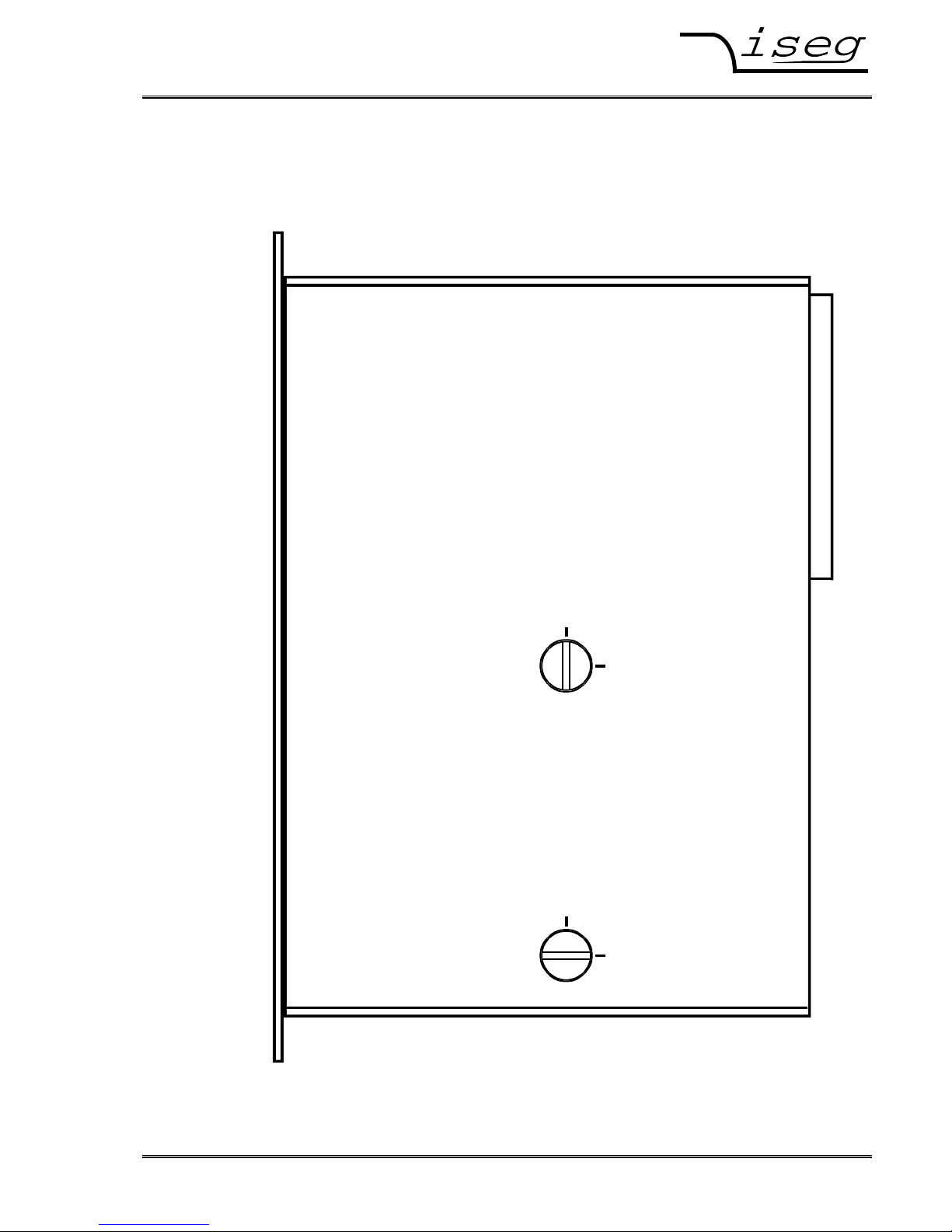
POLARITY
NEG
POS
A
NEG
POS
B
Appendix B: VHQ side cover, Polarity rotary switch
eg.: channel A - Polarity negative
channel B - Polarity positive
 Loading...