

ISD ISD-T360SB Datasheet

Table of Contents
Chapter 1ÑHARDWARE . . . . . . . . . . . . . . . . . . . . . . . . . . . . . 1-1
1.1 PIN ASSIGNMENT . . . . . . . . . . . . . . . . . . . . . . . . . . . . . . . . . . . . . . . . . . . . . . . . . . 1-1
1.1.1 Pin-Signal Assignment . . . . . . . . . . . . . . . . . . . . . . . . . . . . . . . . . . . . . . . . . . . . . . 1-1
1.2 DESCRIPTION . . . . . . . . . . . . . . . . . . . . . . . . . . . . . . . . . . . . . . . . . . . . . . . . . . . . . 1-3
1.2.1 Resetting . . . . . . . . . . . . . . . . . . . . . . . . . . . . . . . . . . . . . . . . . . . . . . . . . . . . . . . . . 1-3
1.2.2 Clocking . . . . . . . . . . . . . . . . . . . . . . . . . . . . . . . . . . . . . . . . . . . . . . . . . . . . . . . . . 1-3
1.2.3 Power-Down Mode . . . . . . . . . . . . . . . . . . . . . . . . . . . . . . . . . . . . . . . . . . . . . . . . 1-4
1.2.4 Power and Grounding . . . . . . . . . . . . . . . . . . . . . . . . . . . . . . . . . . . . . . . . . . . . . 1-5
1.2.5 Memory Interface . . . . . . . . . . . . . . . . . . . . . . . . . . . . . . . . . . . . . . . . . . . . . . . . . 1-6
1.2.6 The Codec Interface . . . . . . . . . . . . . . . . . . . . . . . . . . . . . . . . . . . . . . . . . . . . . 1-13
1.3 SPECIFICATIONS . . . . . . . . . . . . . . . . . . . . . . . . . . . . . . . . . . . . . . . . . . . . . . . . . . 1-18
1.3.1 Absolute Maximum Ratings . . . . . . . . . . . . . . . . . . . . . . . . . . . . . . . . . . . . . . . . 1-18
1.3.2 Electrical Characteristics . . . . . . . . . . . . . . . . . . . . . . . . . . . . . . . . . . . . . . . . . . 1-18
1.3.3 Switching Characteristics—Preliminary . . . . . . . . . . . . . . . . . . . . . . . . . . . . . . . 1-20
1.3.4 Synchronous Timing Tables . . . . . . . . . . . . . . . . . . . . . . . . . . . . . . . . . . . . . . . . . 1-23
1.3.5 Timing Diagrams . . . . . . . . . . . . . . . . . . . . . . . . . . . . . . . . . . . . . . . . . . . . . . . . . 1-25
Chapter 2ÑSOFTWARE . . . . . . . . . . . . . . . . . . . . . . . . . . . . . 2-1
2.1 SYSTEM OPERATION . . . . . . . . . . . . . . . . . . . . . . . . . . . . . . . . . . . . . . . . . . . . . . . . 2-1
2.1.1 The State Machine . . . . . . . . . . . . . . . . . . . . . . . . . . . . . . . . . . . . . . . . . . . . . . . . 2-1
2.1.2 Command Execution . . . . . . . . . . . . . . . . . . . . . . . . . . . . . . . . . . . . . . . . . . . . . . 2-2
2.1.3 Event Handling . . . . . . . . . . . . . . . . . . . . . . . . . . . . . . . . . . . . . . . . . . . . . . . . . . . . 2-2
2.1.4 Message Handling . . . . . . . . . . . . . . . . . . . . . . . . . . . . . . . . . . . . . . . . . . . . . . . . . 2-3
2.1.5 Tone Generation . . . . . . . . . . . . . . . . . . . . . . . . . . . . . . . . . . . . . . . . . . . . . . . . . . 2-4
2.1.6 Initialization and Configuration . . . . . . . . . . . . . . . . . . . . . . . . . . . . . . . . . . . . . . 2-4
2.1.7 Power-Down Mode . . . . . . . . . . . . . . . . . . . . . . . . . . . . . . . . . . . . . . . . . . . . . . . . 2-5
2.2 PERIPHERALS . . . . . . . . . . . . . . . . . . . . . . . . . . . . . . . . . . . . . . . . . . . . . . . . . . . . . . 2-5
2.2.1 Microcontroller interface . . . . . . . . . . . . . . . . . . . . . . . . . . . . . . . . . . . . . . . . . . . 2-5
2.2.2 Memory Interface . . . . . . . . . . . . . . . . . . . . . . . . . . . . . . . . . . . . . . . . . . . . . . . . . 2-8
2.2.3 codec interface . . . . . . . . . . . . . . . . . . . . . . . . . . . . . . . . . . . . . . . . . . . . . . . . . . 2-9
2.3 ALGORITHM FEATURES . . . . . . . . . . . . . . . . . . . . . . . . . . . . . . . . . . . . . . . . . . . . . . 2-9
2.3.1 VCD (Voice Compression and Decompression) . . . . . . . . . . . . . . . . . . . . . . . 2-10
2.3.2 DTMF Detection . . . . . . . . . . . . . . . . . . . . . . . . . . . . . . . . . . . . . . . . . . . . . . . . . . 2-11
2.3.3 Tone and Energy Detection (Call Progress) . . . . . . . . . . . . . . . . . . . . . . . . . . . 2-12
ISD
vii

ISD-T360SB
2.3.4 Full-Duplex Speakerphone . . . . . . . . . . . . . . . . . . . . . . . . . . . . . . . . . . . . . . . . . .2-14
2.3.5 Speech Synthesis . . . . . . . . . . . . . . . . . . . . . . . . . . . . . . . . . . . . . . . . . . . . . . . . .2-16
2.4 VOICEDSP PROCESSOR COMMANDS—QUICK REFERENCE TABLE . . . . . . . . .2-21
2.5 COMMAND DESCRIPTION . . . . . . . . . . . . . . . . . . . . . . . . . . . . . . . . . . . . . . . . . .2-24
Chapter 3ÑSCHEMATIC DIAGRAMS . . . . . . . . . . . . . . . . . . . 3-1
3.1 APPLICATION INFORMATION . . . . . . . . . . . . . . . . . . . . . . . . . . . . . . . . . . . . . . . . .3-1
Chapter 4ÑPHYSICAL DIMENSIONS . . . . . . . . . . . . . . . . . . . 4-1
viii
Voice Solutions in Silicon
™

ISD-T360SB
VoiceDSP™ Digital Speech Processor with
Master/Slave, Full-Duplex Speakerphone, Multiple Flash
—Advance Information—
Preliminary Information
The VoiceDSP™ product family combines multiple digital signal processing functions on a single
chip for cost-effective solutions in telephony, automotive and consumer applications.
The VoiceDSP processor offers necessary features to modern telephony products, such as:
high-quality, speech record and playback, electrical and acoustic echo cancellation for full-duplex hands-free speakerphone operation.
The ISD-T360SB VoiceDSP can be used in various
applications:
¥
Digital telephony with add-on speech
processing: Digital Telephone Answering
Machines(DTADs); and full-duplex, handsfree speakerphone operation for ISDN,
DECT, Digital Spread Spectrum, and
analog cordless applications; CT0/1 Base
stations.
¥
An add-on chip for corded telephones
featuring DTAD functions and/or fullduplex, hands-free speakerphone
operation.
¥
Stand-alone digital answering machines
with full-duplex, hands-free speakerphone
operation.
and ARAM/DRAM Support
Based on ISD’s unique concept which combines
16-bit DSP (Digital Speech Processor) and 16-bit
RISC core technology, the ISD-T360SB is a highperforming chip solution for various applications.
To facilitate incorporating the VoiceDSP processor, it features system support functions such as
an interrupt control unit, codec interface (master, slave), Microwire interface to the system microcontroller, as well as a memory handler for
Flash and DRAM memory devices. Design of
high-end, price optimized systems are possible
with ISD’s VoiceDSP flexible system interfaces
(codec, microcontroller, and memory management support).
The ISD-T360SB processor operates as a peripheral controlled by the system microcontroller via
an enhanced, serial Microwire interface. The system microcontroller typically controls the analog
circuits, buttons and display, as well as activates
functions through commands. The VoiceDSP executes these commands and returns status information to the Microcontroller.
The VoiceDSP software resides in the on-chip
ROM. It includes DSP-based algorithms, system
support functions, and a software interface to
hardware peripherals.
¥
Voice memo recording
¥
Automotive applications employing fullduplex speakerphone operations for
hands-free, in-car communications, and
for car status and information
announcements.
December 1998
ISD · 2045 Hamilton Avenue, San Jose, CA 95125 · TEL: 408/369-2400 · FAX: 408/369-2422 · http://www.isd.com

ISD-T360SB
FEATURES AT A GLANCE
DTAD MANAGEMENT
¥
Highest quality speech recording in PCM
format for music on hold or other OGM
(Out Going Message) recording and IVS
¥
Selectable high-quality speech
compression rate of 5.3 Kbit/s, 9.9 Kbits or
16.8 Kbit/s, plus silence compression with
each rate
¥
Up to 16 minutes recording on a 4-Mbit
Flash
¥
High-quality music compression for music
on hold (16.8 Kbits)
¥
Programmable message tag for message
categorization, e.g., Mailboxes, InComing
Messages (ICM), OutGoing Messages
(OGM)
¥
Message management
¥
Skip forward or backward during message
playback
¥
Variable speed playback
¥
Real-time clock: Day of Week, Hours,
Minutes
¥
Multi-lingual speech synthesis using
International Vocabulary Support (IVS)
¥
Vocabularies available in: English,
Japanese, Mandarin, German, French
and Spanish
¥
Software Automatic Gain Control (AGC)
CALL AND DEVICE MANAGEMENT
¥
Digital volume control
¥
Least cost routing support (LCR)
¥
Power-down mode
¥
3V to 5V selectable power supply
¥
4.096 MHz operation
¥
DTMF generation and detection
¥
Telephone line functions, including busy
and dial tone detection
¥
Single tone generation
¥
DTMF detection during message playback
PERIPHERAL CONTROL
Codec
¥
µ-Law, A-Law, and 16-bit linear codec
input support
¥
Selectable master/slave codec interface
¥
Supports two in-coming lines in slave mode
without speakerphone for DTAD recording
¥
Supports up to 16 user selectable speech
channels in slave mode
¥
Supports long-frame and short-frame
codecs
¥
Single/double bit clock rate for slave
mode
¥
On-chip codec clock generation
SPEAKERPHONE
¥
Digital full-duplex speakerphone
¥
Acoustic- and line-echo cancellation
¥
Continuous on-the-fly monitoring of
external and internal conditions (acoustic
and line) provides high-quality, hands-free,
conversation in a changing environment
¥
Minimum microcontroller control
intervention (Launch-and-forget)
¥
Supports: On, Off, Mute, and Hold
functions
ii
Memory
¥
Supports up to four 4-Mbit, four 8-Mbit, or
four 16-Mbit Flash devices from Toshiba or
Samsung
¥
Supports up to four 16-Mbit ARAM/DRAM
memory devices from Toshiba, Samsung,
and Samsung-compatible
¥
The number of messages that can be
stored is limited only by memory size
¥
Direct access to message memory
Voice Solutions in Silicon
™

ISD-T360SB
¥
Message storage contains all data in a
concatenated chain of memory blocks.
¥
Memory mapping and product floor test
included
¥
Supports external vocabularies, using Flash
memory or expansion ROM
Microwire
¥
MICROWIRE slave interface to an external
microcontroller
¥
Sophisticated command language to
optimize system code size
INTERNATIONAL VOCABULARY SUPPORT (IVS)
For manufacturing recorded voice prompt and
speech synthesis, the ISD International Vocabulary Support delivers pre-recorded voice
prompts in the same high-quality of the user-recorded speech. For complete control over quality and memory management, the IVS features
adjustable speech compressions. In addition,
several pre-recorded voice prompt sets are
available in various languages for further convenience.
Develop a new vocabulary by ISD’s voice
prompt development tool, the ISD-IVS360. This
vocabulary development tool supports various
languages and including their unique grammar
structures. ISD-IVS360, PC-Windows95™-based
program, synthesizes recorded .wav files into the
ISD-T360SB’s various compression rates (including
PCM).
ISD’s VoiceDSP products store IVS vocabularies
on either Flash memory or expansion ROM memories, thus DTAD manufacturers can design a
product for multiple countries, featuring various
languages.
For more details about IVS, refer to the
Guide
.
IVS User’s
Available Languages:
¥
English
¥
Japanese
¥
Mandarin
¥
German
¥
French
¥
Spanish
ISD
iii
ISD-T360SB
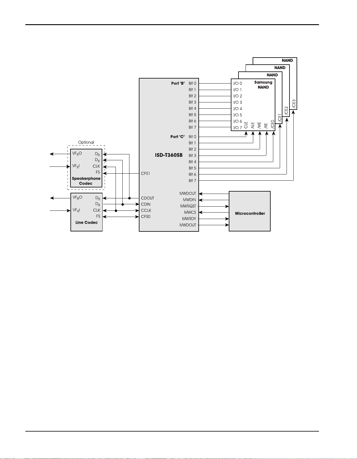
Figure 1-1: ISD-T360SB Block Diagram—Basic Configuration with Four 4Mb/8Mb/16Mb
NAND Flash Devices (Samsung/Toshiba)
iv
Voice Solutions in Silicon
™
ISD-T360SB
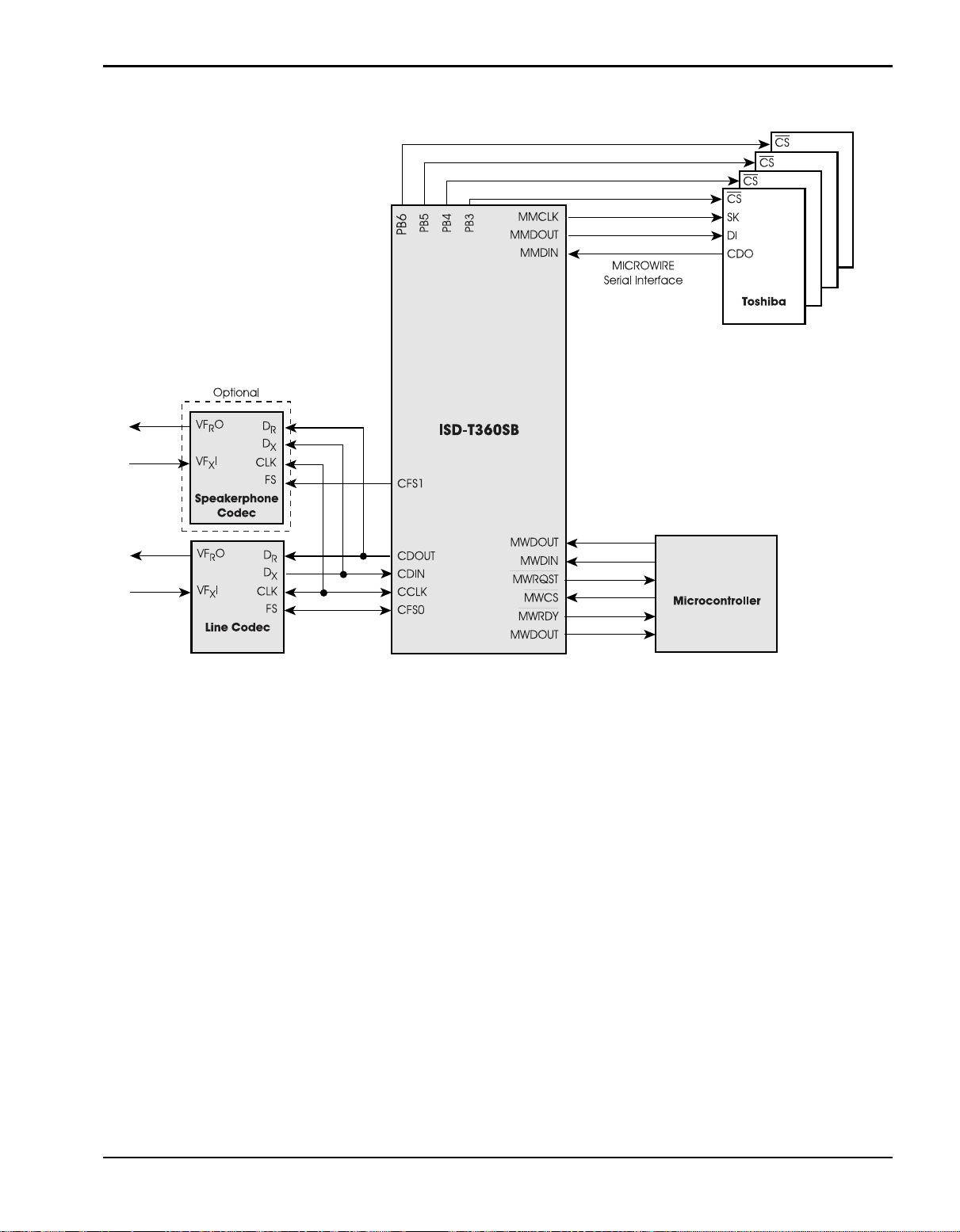
Figure 1-2: ISD-T360SB Block Diagram—Basic Configuration with Four 4Mb Serial Toshiba Flash Devices
ISD
v
ISD-T360SB
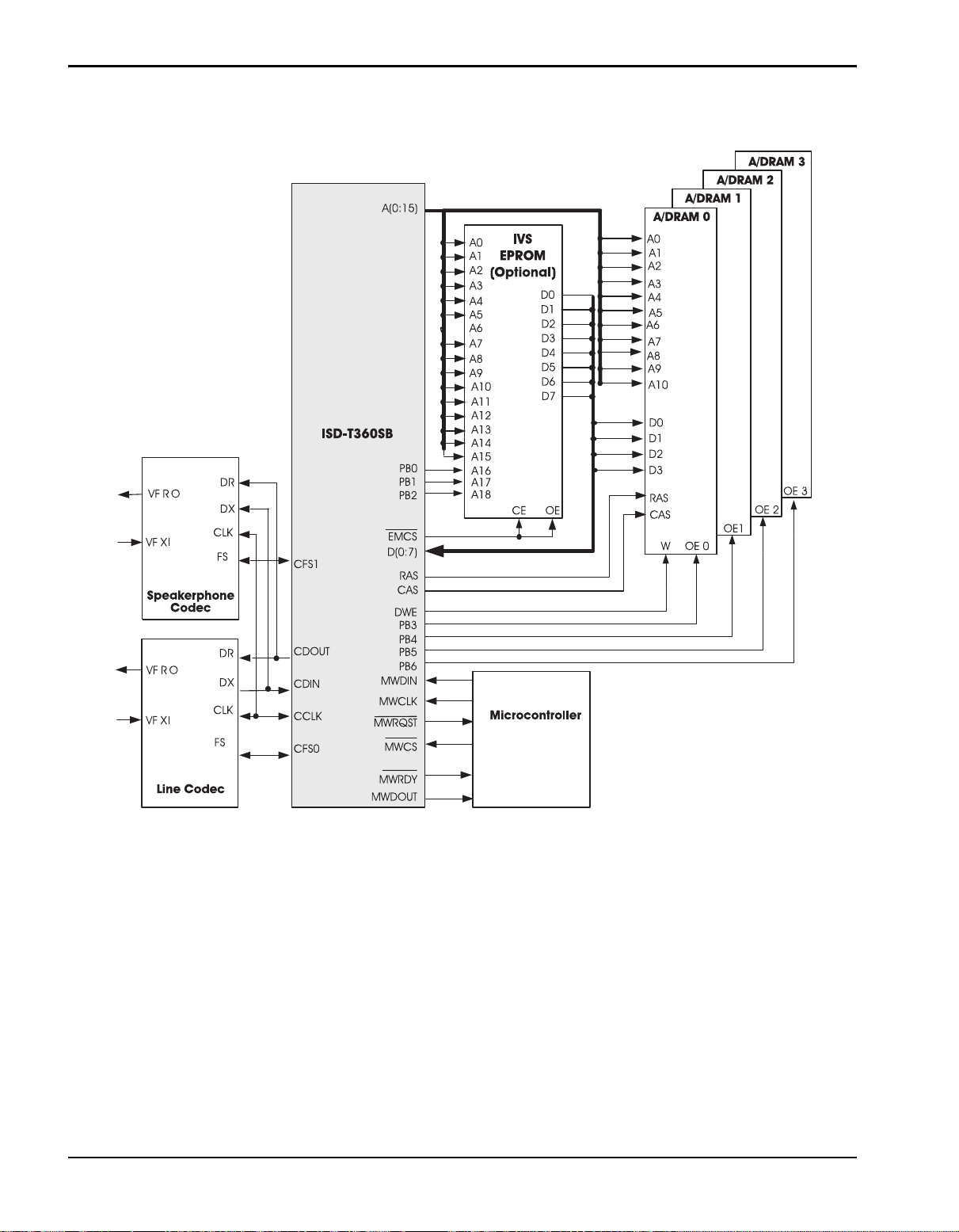
Figure 1-3: ISD-T360SB Block Diagram—Basic Configuration with Four 16Mb ARAM/DRAM Devices
(Samsung) and IVS EPROM
vi
Voice Solutions in Silicon
™

1—HARDWARE
Chapter 1ÑHARDWARE
ISD-T360SB
1.1 PIN ASSIGNMENT
The following sections detail the pins of the ISDT360SB processor. Slashes separate the names of
signals that share the same pin.
Figure 1-1: 80-MQFP Package Connection Diagram
SS
V
A0
A1
ISD-T360SB
RAS
DWE
A9
A10
/MMDOUT
/MMDIN
NC
D0
D1
D2
V
SS
D3
HI
V
CC
V
CC
D4
D5
D6
D7
PC0/A11
NC
NC
NC
1
2
3
4
5
6
7
8
9
10
11
12
13
14
15
16
17
18
19
20
NC
NC
NC
NC
NC
1.1.1 PIN-SIGNAL ASSIGNMENT
Table 1-1 shows all the pins, and the signals that
use them in different configurations. It also shows
the type and direction of each signal.
A
CC
V
A3
A2
80-MQFP
T op Vie w
A4
A5
A6
A7
A8
CC
V
6465666768697071727374757677787980
3736353433323130292827262524232221
V
CC
SS
V
CAS/MMCLK
616263
60
59
58
57
56
55
54
53
52
51
50
49
48
47
46
45
44
43
42
41
403938
VSSA
X2/CLKIN
X1
TST
NC
NC
NC
MWRDY
MWDOUT
NC
V
SS
MWRQST
V
CC
MWCLK
MWDIN
CCLK
CDIN
CFS0
CDOUT
CFS1
ISD
PC2/A13
PC1/A12
PC3/A14
PC5
/ENV0
PC4/A15
PC6/EMCS
PC7
PB0
PB1
V
CC
PB2
SS
V
PB4
PB3
PB5
PB6
PB7
RESET
MWCS
NC
1-1
ISD-T360SB
1—HARDWARE
Table 1-1: VoiceDSP Pin Signal Assignment
Pin Name Signal Name Type Description
A(0:15) A(0:16) Output Address bits 0 through 16
CAS CAS Output DRAM Column Address Strobe
CCLK CCLK I/O Codec Master/slave Clock
CDIN CDIN Input Data Input from Codec
CDOUT CDOUT Output Data Output to Codec
CFS0 CFS0 I/O Codec 0 Frame Synchronization
CFS1 CFS1 Output Codec 1 Frame Synchronization
D(0:7) D(0:7) I/O Data bits 0 through 7
DWE DWE Output DRAM Write Enable
EMCS/ENV0 EMCS Output Expansion Memory Chip Select
EMCS/ENV0 ENV0 Input Environment Select
MMCLK MMCLK Output Master MICROWIRE Clock
MMDIN MMDIN Input Master MICROWIRE Data Input
MMDOUT MMDOUT Output Master MICROWIRE DATA Output
MWCLK MWCLK Input MICROWIRE Clock
MWCS MWCS Input MICROWIRE Chip Select
MWDIN MWDIN Input MICROWIRE Data Input
MWDOUT MWDOUT Output MICROWIRE DATA Output
MWRDY MWRDY Output MICROWIRE Ready
MWRQST MWRQST Output MICROWIRE Request Signal
PB(0:7)
PC(0:7) PB(0:7) I/O Port C, bits 0 through 7
RAS RAS Output DRAM Row Address Strobe
RESET RESET Input Reset
TST TST Input Test pin
V
V
VCCHI VCCHI Power 5 V power supply pin. Connect to VCC if 3.3 V power supply is
V
VSSAV
X1 X1 Oscillator Crystal Oscillator Interface
X2/CLKIN X2 Oscillator Crystal Oscillator Interface
3
CC
AV
CC
SS
PB(0:7) I/O Port B, bits 0 through 7
V
CC
CC
V
SS
A Power Ground for on-chip analog circuitry
SS
Power 3.3 V power supply pin
A Power 3.3 V analog circuitry power supply pin
used.
Power Ground for on-chip logic and output drivers
1.
TTL1 output signals provide CMOS levels in the
steady state, for small loads.
2.
Input during reset. CMOS level input.
3.
Virtual address lines for IVS ROM.
4.
Chip select lines for Serial Flash devices.
5.
Schmitt trigger input.
1-2
Voice Solutions in Silicon
™
1—HARDWARE
1.2 DESCRIPTION
ISD-T360SB
This section provides details of the functional
characteristics of the VoiceDSP processor. It is divided into the following sections:
• Resetting
• Clocking
• Power-Down Mode
• Power and Grounding
• Memory Interface
• Codec Interface
1.2.1 RESETTING
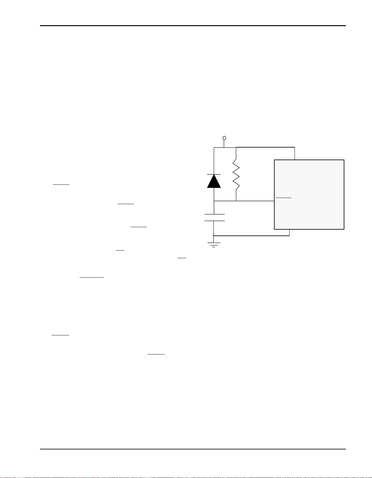
The RESET pin is used to reset the VoiceDSP processor.
On application of power, RESET
for at least t
that all on-chip voltages are completely stable
before operation. Whenever RESET
must also remain active for not less than t
Table 1-10 and Table 1-11. During this period,
and for 100 ms after, the TST
This can be done with a pull-up resistor on the TST
pin.
after VCC is stable. This ensures
pwr
must be held low
is applied, it
, see
RST
signal must be high.
If the load on the ENV0 pin causes the current to
exceed 10 µA, use an external pull-up resistor to
keep the pin at 1.
Figure 1-2 shows a recommended circuit for
generating a reset signal when the power is
turned on.
Figure 1-2: Recommended Power-On Reset
Circuit
V
CC
V
CC
ISD-T360
RESET
V
SS
The value of MWRDY
set period, and for 100 ms after. The microcontroller should either wait before polling the signal
for the first time, or the signal should be pulled
high during this period.
Upon reset, the ENV0 signal is sampled to determine the operating environment. During reset,
the EMCS
nals. An internal pull-up resistor sets ENV0 to 1.
After reset, the same pin is used for EMCS
/ENV0 pin is used for the ENV0 input sig-
is undefined during the re-
.
System Load on ENV0
For any load on the ENV0 pin, the voltage should
not drop below V
Table 1-11).
ISD
(see Table 1-10 and
ENVh
1.2.2 CLOCKING
The VoiceDSP processor provides an internal oscillator that interacts with an external clock
source through the X1 and X2/CLKIN pins. Either
an external single-phase clock signal, or a crystal
oscillator, may be used as the clock source.
External Single-Phase Clock Signal
If an external single-phase clock source is used, it
should be connected to the CLKIN signal as
shown in Figure 1-3, and should conform to the
voltage-level requirements for CLKIN stated in
“ELECTRICAL CHARACTERISTICS” on page 1-18.
1-3

ISD-T360SB
1—HARDWARE
Figure 1-3: External Clock Source
VoiceDSP
X1
X2/CLKIN
Single-phase Clock Signal
Clock Generator
Crystal Oscillator
A crystal oscillator is connected to the on-chip
oscillator circuit via the X1 and X2 signals, as
shown in Figure 1-4.
Figure 1-4: Connections for an External
Crystal Oscillator
Table 1-2 lists the components in the crystal oscillator circuit
Table 1-2: Components of Crystal Oscillator
Circuit
Component V alues Tolerance
Crystal Resonator 4.096 MHz
Resistor R1 10 MΩ 5%
Capacitors C1, C233 pF 20%
1.2.3 POWER-DOWN MODE
Power-down mode is useful during a power failure or in a power-saving model, when the power
source for the processor is a backup battery or in
battery-powered devices, while the processor is
in idle mode.
ISD-T360
X1X2
R1
C2
Keep stray capacitance and inductance, in the
oscillator circuit, as low as possible. The crystal
resonator, and the external components, should
be as close to the X1 and X2/CLKIN pins as possible, to keep the trace lengths in the printed circuit to an absolute minimum.
You can use crystal oscillators with maximum
load capacitance of 20 pF, although the oscillation frequency may differ from the crystal’s specified value.
C1
In power-down mode, the clock frequency of
the VoiceDSP processor is reduced and some of
the processor modules are deactivated. As a result, the ISD-T360SB consumes considerably less
power than in normal-power mode. Although
the VoiceDSP processor does not perform all its
usual functions in power-down mode, it does retain stored messages and maintain the date and
time.
NOTE In power-down mode all the chip select
signals, CS0 to CS3, are set to 1. To guarantee that there is no current flow from these
signals to the Flash devices, the power supply to these devices must not be
disconnected.
The ISD-T360SB stores messages and all memory
management information in Flash or ARAM/
DRAM memory. When Flash memory is used for
memory management, power does not need to
be maintained to the processor to preserve
stored messages. When ARAM/DRAM memory is
used for message management, preserving
stored messages requires a battery back up dur-
1-4
Voice Solutions in Silicon
™
1—HARDWARE
ISD-T360SB
ing a power failure. If the power failure extends
the life of the battery, the microcontroller should
perform the initialization sequence (as described
on page 2-4), and use the SETD command to set
the date and time.
To keep power consumption low during powerdown mode, the RESET
MWDIN signals should be held above V
or below V
+ 0.5 V.
SS
, MWCS, MWCLK and
– 0.5 V
CC
1.2.4 POWER AND GROUNDING
Power Pin Connections
The ISD-T360 can operate over two supply voltage ranges 3.3 V ±10% and 5 V ±10%. The five
power supply pins (V
HI) must be connected as shown in
V
CC
, VSS, VCCA, VSSA and
CC
Figure 1-5 when operating in a 3.3 V environment, and as shown in Figure 1-6 when operating in a 5 V environment. Failure to correctly
connect the pins may result in damage to the
device.
The Capacitor and Resistor values are given in
Table 1-3.
Table 1-3: Components of Supply Circuit
Component Values Tolerance
Resistor R1, R2 10 Ω 5%
Capacitors
Capacitors C3, C4,
C5, C6, C7
1.
All capacitors represent two parallel capacitors at
the values 1.0 µF and 0.1 µF.
(1)
C1, C2
1.0 µF
Tantalum
0.1 µF Ceramic
20%
Figure 1-5: 3.3 V Power Connection Diagram
R
3.3 V Supply
V
SS
VCCHI
V
CC
V
V
SS
CC
74 72 64 63 61
9
11
12
V
CC
VCCAV
V
CC
ISD-T360
30 32
V
1
C
SS
60
50
48
SS
VSSA
V
SS
V
CC
1
ISD
1-5
ISD-T360SB
Figure 1-6: 5 V Power Connection Diagram
C
6
R
C
5
2
1—HARDWARE
VSSV
CC
V
5 V Supply
C
2
VCCHI
V
74 72 64 63 61
SS
9
11
CC
12
30 32
V
CC
For optimal noise immunity, the power and
ground pins should be connected to V
CC
and
the ground planes, respectively, on the printed
circuit board. If V
and the ground planes are
CC
not used, single conductors should be run directly from each V
pin to a power point, and from
CC
each GND pin to a ground point. Avoid daisychained connections. The VoiceDSP does not
perform its usual functions in power-down mode
but it still preserves stored messages, maintains
the time of day and generates ARAM/DRAM refresh cycles.
When you build a prototype, using wire-wrap or
other methods, solder the capacitors directly to
the power pins of the VoiceDSP processor socket, or as close as possible, with very short leads.
V
VCCA
CC
ISD-T360
C
3
V
V
C
SS
7
VSSA
60
V
SS
50
C
48
V
CC
SS
4
1.2.5 MEMORY INTERFACE
Flash Support
The ISD-T360SB VoiceDSP supports Flash devices
for storing recorded data, thus, power can be
disconnected to the ISD-T360SB without losing
data. The ISD-T360SB supports serial and semiparallel Flash device interfaces, such as
TC58V16BFT, TC5816BFT, TC58A040F, KM29N040T,
KM2928000T/IT, and KM29216000AT/AIT. The ISDT360SB may be connected to up to four Flash devices, resulting with maximum recording storage
of 16-Mbits x 4 = 64 Mbits (up to 4 hours of recording time).
The following flash devices are supported:
1-6
Voice Solutions in Silicon
™

1—HARDWARE
ISD-T360SB
Table 1-4: Supported Flash Devices
Manufacturer
Toshiba TC58V16BFT 2Mx8 3.3 V 16-Mbit LV µ-Law
Toshiba TC5816BFT 2Mx8 5 V 16-Mbit A-Law
Toshiba TC58A040F Serial 5V 4-Mbit µ-Law, A-Law
Samsung KM29N040T 512Kx8 5 V 4-Mbit µ-Law, A-Law,
Samsung KM29W8000T/IT 1Mx8 5 V 8-Mbit µLaw
Samsung KM29W16000AT
Memory Device
Name
/AIT
Characteristics
2Mx8 5 V 16-Mbit A-Law
Internal Memory Organization
The Flash devices detailed in Table 1-4 divide internally into basic 4-Kbyte block units. The ISDT360SB uses one block on each device for memory management, leaving the rest of the blocks
available for recording. Using at least one block
for a single recorded message yields a maximum
of NUM_OF_BLOCKS_IN_MEM – 1 (see Table 2-10
for parameter definition) messages per device.
Upon initialization the ISD-T360SB activates a sifting algorithm to detect defected blocks. Defected blocks are defined as blocks with over 10
bad nibbles (a nibble consists of 4 bits). The defected blocks are marked as UNUSED and excluded from the list of available blocks for
recording.
Operating
Voltage
Memory Size Conversion T ype
LV
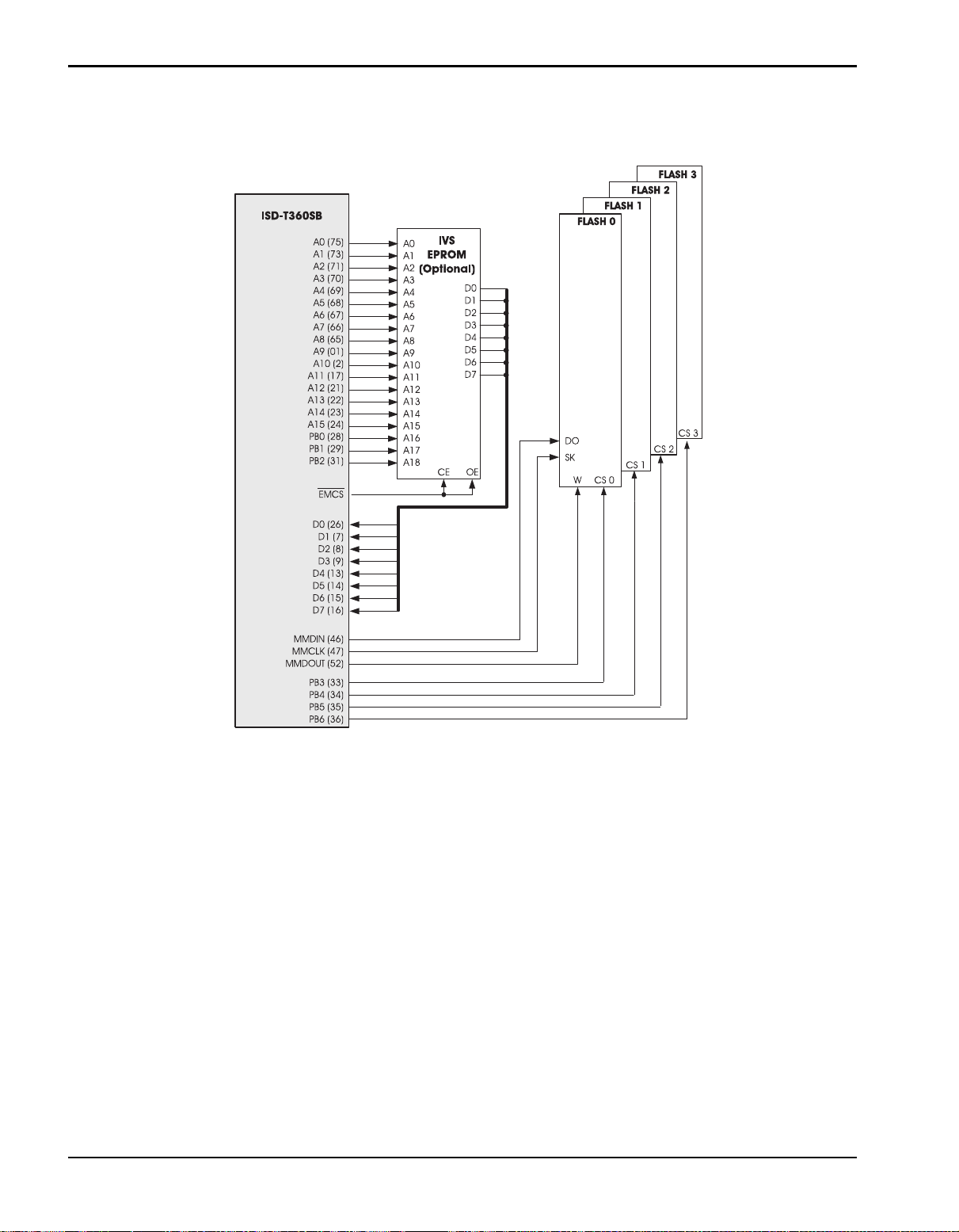
Toshiba Serial Flash
The VoiceDSP processor supports up to four
TC58A040F, 4Mbit, serial interface, Flash memory
devices for storing messages. The TC58A040F is
organized as an array of 128 blocks, with a dedicated, read-only, bad block map programmed
by the manufacturer and located in the last
block. This map is used by the ISD-T360SB to define the available blocks for recording. The ISDT360SB uses the VoiceDSP master MICROWIRE interface to communicate, serially, with the Flash
devices, while selecting the current Flash device
using PB3-PB6. Connecting less than four Flash
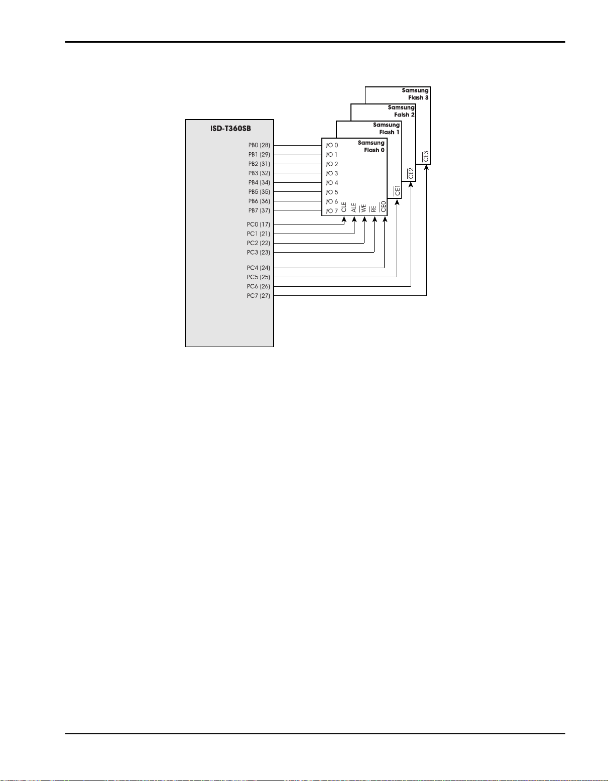
devices require connecting the Flash devices sequentially, starting from PB3 up to PB6 (see
Figure 1-7). Refer to Figure 1-34for the Master MICROWIRE timing diagram.
ISD
1-7
ISD-T360SB
1—HARDWARE
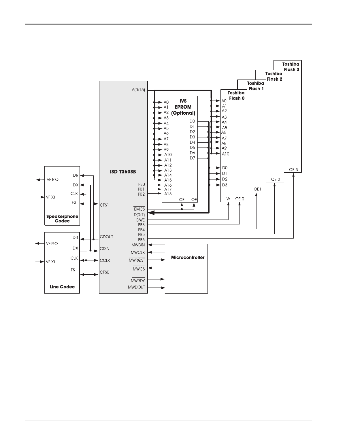
Figure 1-7: Memory Interface with Four Toshiba 4Mbit Serial Flash Devices and
Optional Voice IVS EPROM
1-8
Voice Solutions in Silicon
™
1—HARDWARE
ISD-T360SB
Figure 1-8: Memory Interface with Four 4MB/16 Mbit, NAND Flash Devices (Samsung, Toshiba)
NAND Flash (Samsung, Toshiba)
The VoiceDSP processor supports up to four,
semi-parallel interface, Flash memory devices for
storing messages. Flash device with semi-parallel
interface uses a single 8bit I/O port to set the address and access the data. The ISD-T360SB supports three types of Flash volumes (4Mbit, 8Mbit
and 16Mbit as listed in Table 1-4) while all the
connected Flash devices must be of the same
type. Ports B and C are used to connect ISDT360SB to the Flash devices using port B for address and data transfer and port C for communication control and chip select. Connecting less
than four Flash devices require connecting the
Flash devices sequentially, starting from PC4 up
to PC7 (see Figure 1-8). The ISD-T360SB scans the
Flash devices upon initialization, sifting out the
bad blocks, and marking them in a special map,
located in the last block of each device.
ISD
1-9
ISD-T360SB
1—HARDWARE
Figure 1-9: Memory Interface with Four Toshiba 4Mbit Serial Flash Devices and
Optional IVS EPROM
Flash Endurance
A Flash memory may be erased a limited number of times. To maximize the Flash use, the memory manager utilizes the Flash’s blocks evenly
(i.e., each block is erased more or less the same
number of times), to ensure that all blocks have
the same lifetime. Refer to the respective Flash
memory device data sheets for specific endurance specifications.
A VoiceDSP processor message uses at least one
block.
1-10
The maximum recording time depends on four
factors:
1. The basic compression rate (5.3 Kbit/s,
9.9Kbit/s, or 16.8Kbit/s).
2. The amount of silence in the recorded
speech.
3. The number of bad blocks.
Voice Solutions in Silicon
™
1—HARDWARE
ISD-T360SB
The number of recorded messages. (The basic
memory allocation unit for a message is a 4Kbyte block, which means that half a block on
average is wasted per recorded message).
Table 1-5: Recording Time with 15% Silence
Compression
Memory Size
4 Mbit 5.3 Kbit/s 14.9 Minutes
4 Mbit 9.9 Kbit/s 8.1 Minutes
4 Mbit 16.8 Kbit/s 4.8 Minutes
8 Mbit 5.3 Kbit/s 29.8 Minutes
8 Mbit 9.9 Kbit/s 16.2 Minutes
8 Mbit 16.8 Kbit/s 9.6 Minutes
16 Mbit 5.3 Kbit/s 59.6 Minutes
16 Mbit 9.9 Kbit/s 32.4 Minutes
16 Mbit 16.8 Kbit/s 19.2 Minutes
32 Mbit 5.3 Kbit/s 119.2 Minutes
32 Mbit 9.9 Kbit/s 64.8 Minutes
32 Mbit 16.8 Kbit/s 38.4 Minutes
Compression
Rate
Total Recording
Time
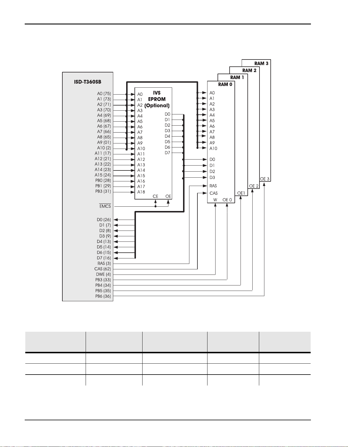
ARAM/DRAM Support
The VoiceDSP processor supports up to four,
16-Mbit, ARAM/DRAM devices for storing messages. The ISD-T360 connects to the ARAM/
DRAM device using address buses A0–A11 and
data buses D0–D3. This connection allows ac-
22
cess to 2
nibbles (16-Mbit) on each device. The
ISD-T360SB selects the current ARAM/DRAM device using PB3–PB6 as described in Figure 1-10.
Using less than four ARAM/DRAM devices requires connecting the devices sequentially,
starting from PB3 up to PC6. RAS
and CAS are
connected in parallel to all the ARAM/DRAM devices and are used to refresh the memory. The
difference between ARAM and DRAM resides
with the amount of bad cells on the device and
the device performance. While DRAM has no
bad cells, ARAM contains certain level of impurity and thus requires testing and mapping of the
bad blocks upon the initialization of the ISDT360SB. Although there are no real blocks on the
ARAM device, the ISD-T360SB emulates virtual
“blocks” on the ARAM device (as if it was a Flash
device), tests these “blocks” and marks them in
a special map on the last “block” on each device. This test is required only when using ARAM
devices (as opposed to DRAM devices that require no testing due to lack of bad blocks). The
virtual division to blocks simplifies the use of
ARAM/DRAM devices and allows the use of the
same set of commands for Flash and ARAM/
DRAM.
Another major difference between ARAM/
DRAM and Flash devices is that the internal mapping in the ARAM is lost upon power off. Thus, the
initialization process needs to take place after
each power reset. The mapping is not lost when
entering and exiting the Power-Down Mode.
Refer to Figure 1-24 through Figure 1-28 for Timing
Diagrams of ARAM/DRAM Read, Write, Refresh in
Normal Mode and Refresh in Power-Down Mode
Cycles.
ROM Interface
IVS vocabularies can be stored in either Flash
memory and/or ROM. The VoiceDSP processor
supports IVS ROM devices through an Expansion
Memory mechanism. Up to 64 Kbytes (64K x 8) of
Expansion Memory are directly supported. Nevertheless, the processor uses bits of the on-chip
port (PB) to further extend the 64 Kbytes address
space up to 0.5 Mbytes address space.
ROM is connected to the VoiceDSP processor using the data bus, D(0:7), the address bus,
A(0:15), the extended address signals, EA(16:18),
and Expansion Memory Chip Select, EMCS
, controls. The number of extended address pins to
use may vary, depending on the size and configuration of the ROM. ISD-T360SB configured with
semi-parallel Flash memory can not support extension ROM.
ISD
1-11
ISD-T360SB
1—HARDWARE
Figure 1-10: Memory Interface with Four 16-Mbit ARAM/DRAM Devices (Samsung, Toshiba) and
Optional IVS EPROM
Table 1-6: Supported DRAM Devices
Manufacturer
Samsung KM44C4004CS-6 EDO 4Mx4 5 V 16-Mbit EDO LV
Samsung KM44V4004CS-6 EDO 4Mx4 3.3 V 16-Mbit EDO
Toshiba TP EDO 4Mx4 5V, 3.3V 16-Mbit EDO, LV
1-12
Memory Device
Name
Characteristics Operating V oltage Memory Size
Voice Solutions in Silicon
™

1—HARDWARE
1.2.6 THE CODEC INTERFACE
ISD-T360SB
The ISD-T360 provides an on chip interface for
analog and digital telephony, supporting master
and slave codec interface modes. In master
mode, the ISD-T360 controls the operation of the
codec for use in analog telephony. In the slave
mode, the ISD-T360 codec interface is controlled
by an external source. This mode is used in digital
telephony (i.e., ISDN or DECT lines). The slave
mode is implemented with respect to IOM-2™/
CGI specifications.
See Table 1-7 for codec options for the ISDT360SB (ISD supports compatible codecs in addition to those listed below).
The codec interface supports the following features:
• Master Mode or Slave Mode.
• 8- or 16-bit Channel Width.
• Long (Variable) or Short (Fixed) Frame
Protocol.
• Single or Double Bit (Slave Mode Only)
Clock Rate.
• Single or Dual Channel Codecs
• One or Two Codecs
• Multiple Clock And Sample Rates.
• One or Two Frame Sync Signals
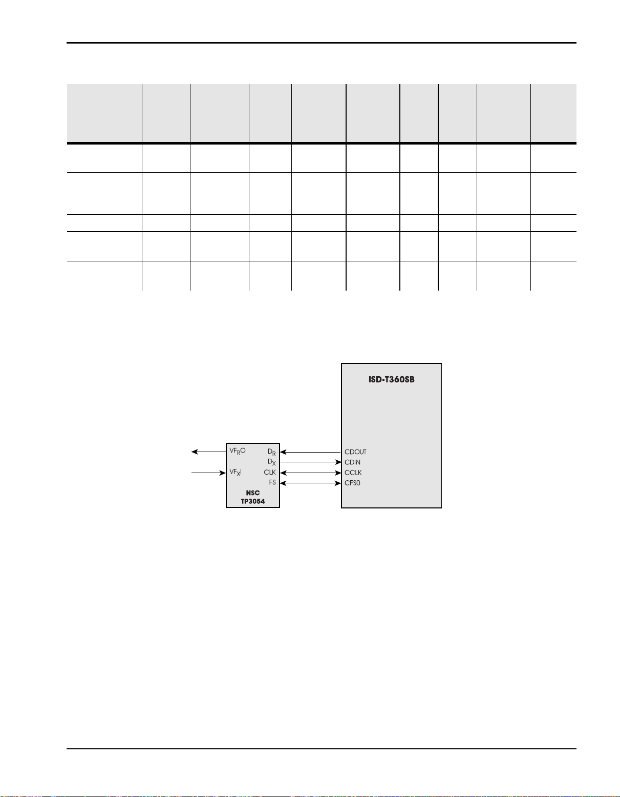
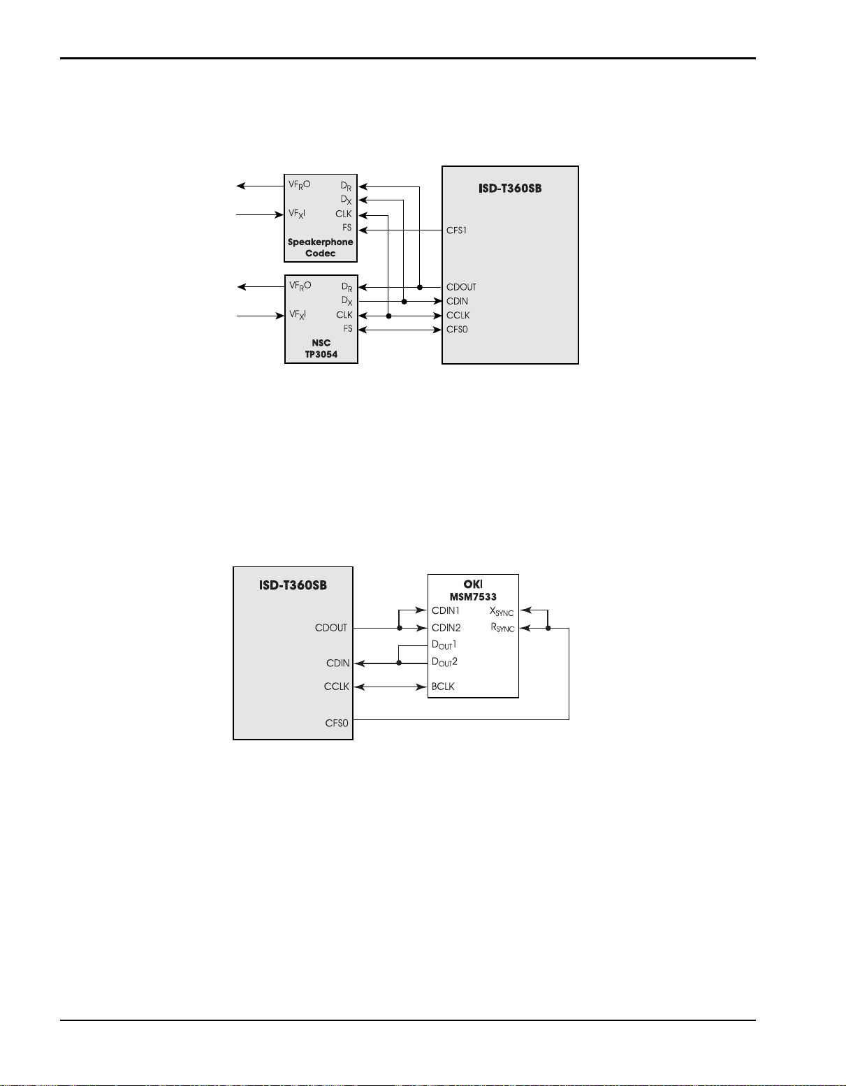
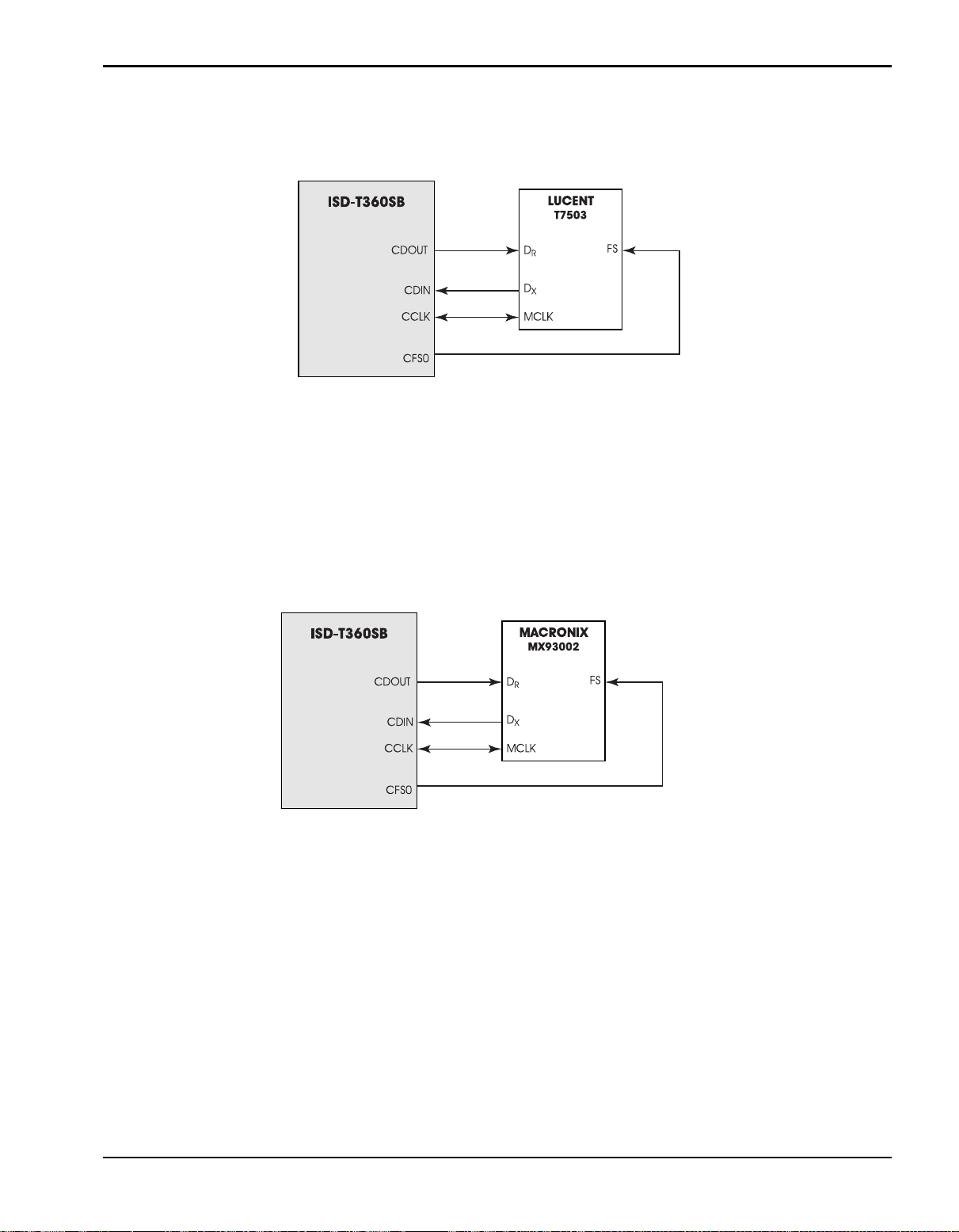
This codec interface uses five signals: CDIN, CDOUT, CCLK, CFS0, and CFS1. The CDIN, CDOUT,
CCLK, and CFS0 pins are connected to the first
codec. The second codec is connected to
CDIN, CDOUT, CCLK, and CFS1 pins. Data is
transferred to the codec through the CDOUT
output pin. Data is read from the codec through
the CDIN input pin. The CCLK and CFS0 pins are
output in Master Mode and input in Slave Mode.
The CFS1 is an output pin.
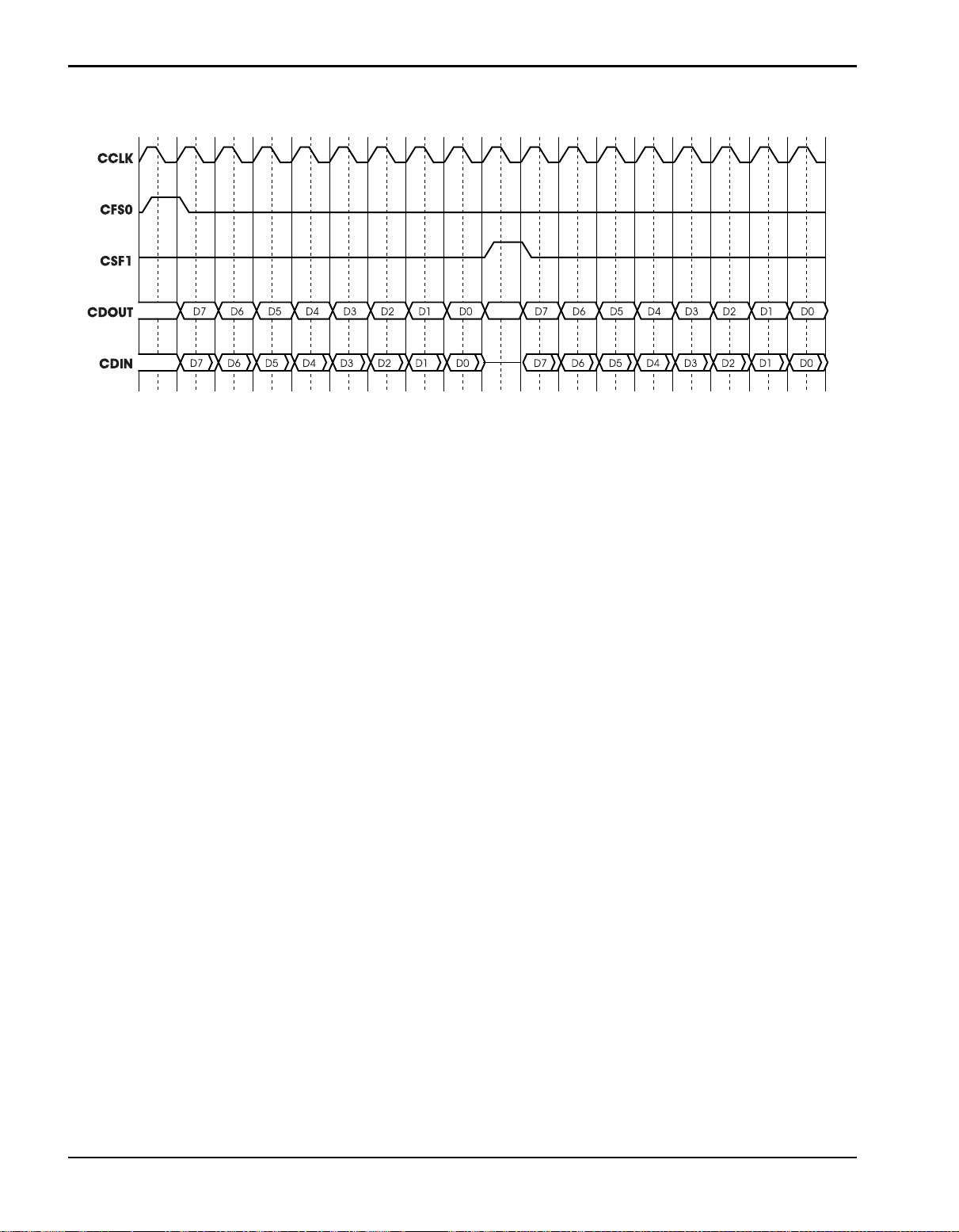
Short Frame Protocol
When the short frame protocol is configured,
eight or sixteen data bits are exchanged with
each codec in each frame (i.e., the CFS0 cycle).
Data transfer begins when CFS0 is set to 1 for one
CCLK cycle. The data is then transmitted, bit by
bit, via the CDOUT pin. Concurrently, the received data is shifted in through the CDIN pin.
Data is shifted one bit per CCLK cycle. After the
last bit has been shifted, CFS1 is set to 1 for one
CCLK cycle. Then, the data from the second codec is shifted out via CDOUT, concurrently with
the inward shift of the data received via CDIN.
Long Frame Protocol
When long frame protocol is configured, eight or
sixteen data bits are exchanged with each codec, as for the short frame protocol. However,
for the long frame protocol, data transfer starts
by setting CFS0 to 1 for eight or sixteen CCLK cycles. Short or long frame protocol is available in
both Master and Slave modes. Figure 1-11 illustrates an example of short frame protocol with
an 8-bit channel width.
Table 1-7: Supported Codec Devices
Manufacturer Codec Device Name Characteristics Operating Voltage Conversion T ype
National
Semiconductor
National
Semiconductor
Oki MSM7533V Dual codec 5 V µ-Law, A-Law
Oki MSM 7704 Dual codec 3.3 V µ-Law, A-Law, LV
Macronix MX93002FC Dual codec 5 V µ-Law
Lucent T7502 Dual codec 5 V A-Law
Lucent T7503 Dual codec 5 V µ-Law
ISD
TP3054 Single codec 5 V µ-Law
TP 3057 Single codec 5 V A-Law
1-13
ISD-T360SB
1—HARDWARE
Figure 1-11: Codec Protocol-Short Frame—8-Bit Channel Width
Channel Width
The Codec interface supports both 8-bit and 16bit channel width in Master and Slave Modes.
Slave Mode
The VoiceDSP supports digital telephony applications including DECT and ISDN by providing a
Slave Mode of operation. In Slave Mode operation, the CCLK signal is input to the ISD-T360 and
controls the frequency of the codec interface
operation. The CCLK may take on any frequency between 500 KHz and 4 MHz. Both long and
short frame protocol are supported with only the
CFS1 output signal width affected. The CFS0 input signal must be a minimum of one CCLK cycle.
In slave mode, a double clock bit rate feature is
available as well. When the codec interface is
configured to double clock bit rate, the CCLK input signal is divided internally by two and the resulting clock used to control the frequency of the
codec of the codec interface operation.
This interface supports ISDN protocol with one bit
clock rate or double bit clock rate. The exact format is selected with the CFG command. The
slave codec interface uses four signals: CDIN,
CDOUT, CCLK, and CFS0. The CDIN, CCLK, and
CFS0 input pins and the CDOUT output pins are
connected to the ISDN/DECT agent. Data is
transferred to the VoiceDSP through the CDIN
pin and read out through the CDOUT pin. The
CFS0 pin is used to define the start of each frame
(see below) the source of that signal is at the
master side. The CCLK is used for bit timing of
CDIN and CDOUT. The rate of the CCLK is configured via the CFG command and can be twice
of the data rate or at the data rate. The source
of that signal is at the master side.
1-14
Voice Solutions in Silicon
™
1—HARDWARE
ISD-T360SB
Table 1-8: Typical Codec Applications
Application
Analog µLaw
ISDN—8 bit
digital—ALaw
Linear single 1 Master 16 short 1 2.048 8000 1
IOM-2/GCI single
266
Compatibility
Codec
Type
single 1 Master 8 short or
dual 2 Slave 8 short 1 or 2 2.048 8000 1
or dual
single
or dual
No. of
Channels
1–2 Slave 8 short 1 or 2 1.536 8000 1
1 or 2 Master 8 long or
Master/
Slave
Channel
Width
(No. Bits)
Long/
Short
Frame
Protocol
long
short
CCLK
Bit Rate
1 2.048 8000 1
1 2.048 8000 1 or 2
Freq.
(MHz)
Sample
Rate (Hz)
No. of
Frame
Syncs
Figure 1-12: Codec Interface with One Single Codec, NSC TP3054, for Single Line Operation
ISD
1-15
ISD-T360SB
1—HARDWARE
Figure 1-13: Codec Interface Diagram with Two, Single Codecs, NSC TP3054, and NSC TP3057, for
Speakerphone Operation
Figure 1-14: Codec Interface for Dual Line or Single Line and Speakerphone Operation
with OKI Dual Codec
1-16
Voice Solutions in Silicon
™
1—HARDWARE
Figure 1-15: Codec Interface for Dual Line or Single Line and Speakerphone
ISD-T360SB
with Lucent Dual Codec
Figure 1-16: Codec Interface for Dual Line or Single Line and Speakerphone Operation
with Macronix Dual Codec
ISD
1-17
ISD-T360SB
1.3 SPECIFICATIONS
1—HARDWARE
1.3.1 ABSOLUTE MAXIMUM RATINGS
NOTE Absolute maximum ratings indicate limits
beyond which permanent damage may
Storage temperature –65˚C to +150˚C
Temperature under bias 0˚C to +70˚C
occur. Continuous operation at these limits
is not intended; operation should be limited
to the conditions specified below.
All input and output
–0.5 V to +6.5 V
voltages with respect to
GND
1.3.2 ELECTRICAL CHARACTERISTICS
TA = 0ºC to +70ºC, VCC = 5 V ±10% Or 3.3 V ±10%, GND = 0 V
Table 1-9: Electrical Characteristics—Preliminary Information
(All Parameters with Reference to V
Symbol Parameter Conditions Min Typ Max Units
C
I
CC1
I
CC2
I
CC3
X
X1 and X2 Capacitance
Active Supply Current Normal Operation Mode,
Standby supply current Normal Operation Mode, DSPM
Power-down Mode Supply
Current
I
L
I
(Off) Output Leakage Current
O
Input Load Current 0 V ≤ VIN ≤ V
(I/O pins in Input Mode)
t
CASa
t
CASh
t
CASia
t
CASLw
t
DWEa
t
DWEh
t
DWEia
t
RASa
t
RASh
t
RASia
t
RASLw
t
RLCL
t
WRa
CAS Active After R.E. CTTL, T1 or T2W3 12.0
CAS Hold After R.E. CTTL 0.0
CAS Inactive After R.E. CTTL, T3 or TERF 12.0
DRAM, PDM, CAS Width At 0.8 V, Both Edges 600.0
DWE Active After R.E. CTTL, T2W2 12.0
DWE Hold After R.E. CTTL 12.0
DWE Inactive After R.E. CTTL, T3 12.0
RAS Active After R.E. CTTL, T2W1 or T2WRF 12.0
RAS Hold After R.E. CTTL 0.0
RAS Inactive After R.E. CTTL, T3 or T3RF 12.0
DRAM PDM, RAS Width At 0.8 V, Both Edges 200.0
DRAM PDM RAS Low, after
Low
CAS
WR0 Active After R.E. CTTL, T1 t
1
Running Speech Applications
2
Idle
Power-down Mode
0 V ≤ V
F.E. CAS
≤ V
OUT
to F.E. RAS 200.0
2,3
CC
CC
CC
2
= 3.3 V)
17.0 pF
40.0 80.0 mA
30.0 mA
0.7 mA
–5.0 5.0 µA
–5.0 5.0 µA
/2+2
CTp
1-18
Voice Solutions in Silicon
™
1—HARDWARE
ISD-T360SB
Table 1-9: Electrical Characteristics—Preliminary Information
(All Parameters with Reference to V
Symbol Parameter Conditions Min Typ Max Units
t
WRCSh
t
WRh
t
WRia
V
ENVh
V
Hh
WR0 Hold after EMCS
WR0 Hold After R.E. CTTL t
WR0 Inactive After R.E. CTTL, T3 t
ENV0 Input, High Voltage 2.0 V
CMOS Input with Hysteresis,
Logical 1 Input Voltage
V
Hl
CMOS Input with Hysteresis,
Logical 0 Input Voltage
V
Hysteresis Loop Width
Hys
V
IH
TTL Input, Logical 1 Input
Voltage
V
IL
TTL Input, Logical 0 Input
Voltage
V
OH
Logical 1 TTL, Output
Voltage
V
OHWC
MMCLK, MMDOUT and
Logical 1, Output
EMCS
Voltage
V
OL
Logical 0, TTL Output
Voltage
V
OLWC
MMCLK, MMDOUT and
Logical 0, Output
EMCS
Voltage
V
XH
V
XL
CLKIN Input, High Voltage External Clock 2.0 V
CLKIN Input, Low Voltage External Clock 0.8 V
4
1
R.E. EMCS R.E. to R.E. WR0 10.0
IOH = –0.4 mA 2.4 V
I
= –0.4 mA 2.4 V
OH
I
= –50 µA
OH
5
IOL = 4 mA 0.45 V
I
= 50 µA
OL
I
= 4 mA 0.45 V
OL
I
= 50 µA
OL
5
5
= 3.3 V)
CC
/2–6
CTp
/2+2
CTp
2.1 V
0.8 V
0.5 V
2.0 VCC+0.5 V
–0.5 0.8 V
VCC–0.2 V
0.2 V
0.2 V
1.
Guaranteed by design.
2.
I
=0, TA 25˚C, VCC = 3.3 V for VCC pins and 3.3 V or 5 V on V
OUT
running from internal memory with Expansion Memory disabled.
3.
All input signals are tied to 0 (above VCC – 0.5 V or below VSS + 0.5 V), except ENV0, which is tied to VCC.
4.
Measured in power-down mode. The total current driven, or sourced, by all the VoiceDSP processor’s output signals
is less than 50 µA.
5.
Guaranteed by design, but not fully tested.
ISD
pins, operating from a 4.096 MHz crystal and
CCHI
1-19
ISD-T360SB
1.3.3 SWITCHING CHARACTERISTICS—PRELIMINARY
1—HARDWARE
Definitions
All timing specifications in this section refer to
0.8 V or 2.0 V on the rising or falling edges of the
signals, as illustrated in Figure 1-17 through
Figure 1-23, unless specifically stated otherwise.
Figure 1-17: Synchronous Output Signals (Valid, Active and Inactive)
CTTL or
MWCLK
Signal
2.0V
t
Signal
Maximum times assume capacitive loading of
50pF. CLKIN crystal frequency is 4.096 MHz.
NOTE CTTL is an internal signal and is used as a ref-
erence to explain the timing of other
signals. See Figure 1-37.
2.0V
0.8V
NOTE:
NOTE:
Signal valid, active or inactive time, after a rising edge of CTTL or MWCLK.
Figure 1-18: Synchronous Output Signals (Valid)
MWCLK
Signal
Signal valid time, after a falling edge of MWCLK.
0.8V
t
2.0V
0.8V
Signal
1-20
Voice Solutions in Silicon
™
1—HARDWARE
Figure 1-19: Synchronous Output Signals (Hold), after Rising Edge of CTTL
CTTL
Signal
2.0V
t
Signal
ISD-T360SB
2.0V
0.8V
NOTE:
NOTE:
Signal hold time, after a rising edge of CTTL.
Figure 1-20: Synchronous Output Signals (Hold), after Falling Edge of MWCLK
MWCLK
Signal
Signal hold time, after a falling edge of MWCLK.
2.0V
t
Signal
2.0V
0.8V
Figure 1-21: Synchronous Input Signals
NOTE:
ISD
CTTL or
2.0 V
MWCLK
2.0 V
2.0 V
Signal
0.8 V
t
Signal
Signal setup time, before a rising edge of CTTL or MWCK, and signal hold time after a rising edge of CTTL or MWCK
Setup t
Signal
0.8 V
Hold
1-21
ISD-T360SB
Signal A
Signal B
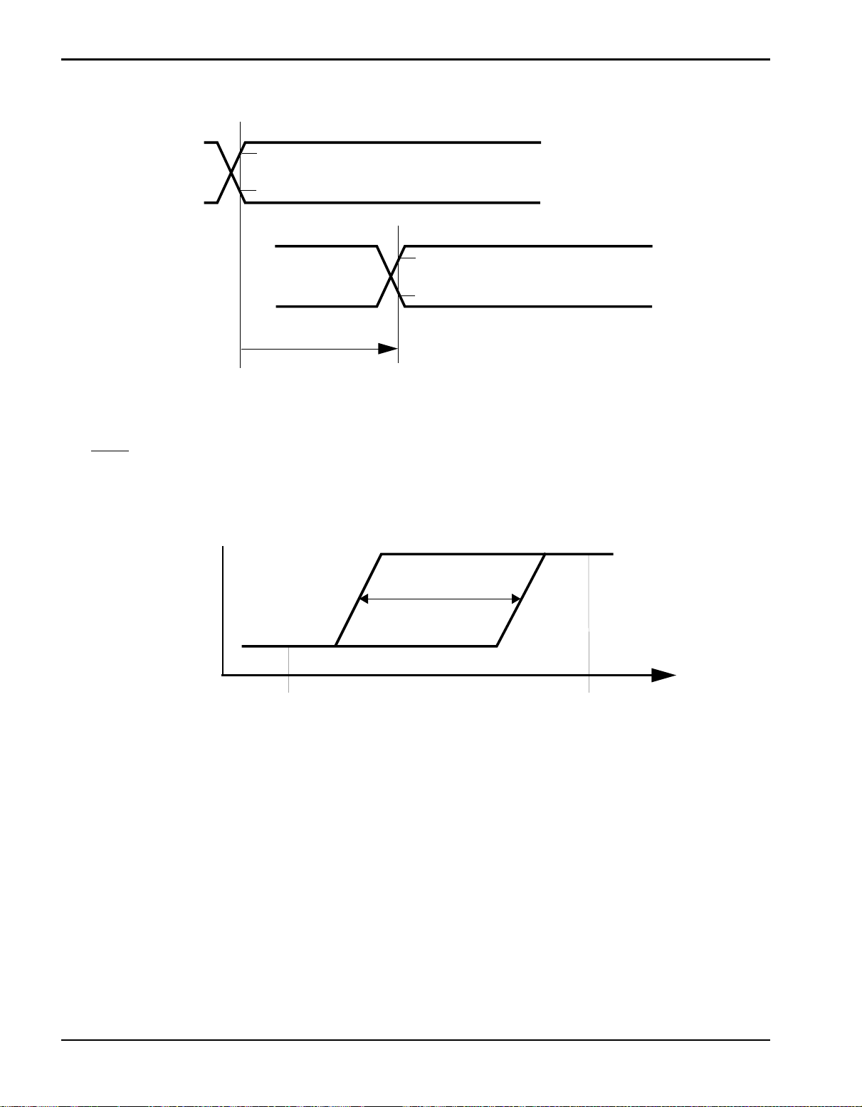
Figure 1-22: Asynchronous Signals
2.0 V
0.8 V
2.0 V
0.8 V
t
Signal
1—HARDWARE
NOTE:
Signal B starts after rising or falling edge of signal A.
The RESET has a Schmitt trigger input buffer. Figure 1-23 shows the input buffer characteristics.
Figure 1-23: Hysteresis Input Characteristics
V
out
V
Hys
V
Hl
V
Hh
1-22
Voice Solutions in Silicon
™
 Loading...