

ISD ISD1020AX, ISD1020API, ISD1020AP, ISD1020AGI, ISD1020AG Datasheet
...
Single-Chip Voice Record/Playback Devices
FEATURES
• Easy-to-use single-chip voice Record/Playback solution
• High-quality, natural voice/audio
reproduction
• Manual switch or microcontroller compatible
– Playback can be edge- or level-
activated
• Single-chip durations of 16 and 20 seconds
• Directly cascadable for longer durations
• Power-down mode
–1 µA standby current (typical)
• Zero-power message storage
– Eliminates battery backup circuits
ISD1000A Series
16- and 20-Second Durations
• Fully addressable to handle multiple
messages
• 100-year message retention (typical)
• 100,000 record cycles (typical)
• On-chip clock source
• No algorithm development required
• Single +5 volt supply
• Available in die form, DIP, and SOIC
packaging
• Industrial temperature (-40°C to +85°C)
version available
®
1
ISD1000A SERIES SUMMARY
Part
Number
ISD1016A 16 8 3.4
ISD1020A 20 6.4 2.7
Information Storage Devices, Inc.
Duration
(Seconds)
Input Sample
Rate (KHz)
Typical Filter
Pass Band
(KHz)
1–1
ISD1000A Series
Product Data Sheets
GENERAL DESCRIPTION
Information Storage Devices’ ISD1000A ChipCorder® Series provides high-quality, single-chip
record/playback solutions for 16- and 20-second
messaging applications. The CMOS devices
include an on-chip oscillator, microphone preamplifier, automatic gain control, antialiasing filter,
smoothing filter, and speaker amplifier. In addition, the ISD1000A Series is fully microprocessorcompatible, allowing complex messaging and
addressing to be achieved.
Recordings are stored in on-chip nonvolatile
memory cells, providing zero-power message
storage. This unique, single-chip solution is made
possible through ISD's patented multilevel storage technology. Voice and audio signals are
stored directly into memory in their natural form,
-1
providing high-quality, solid-state voice reproduction.
DETAILED DESCRIPTION
The ISD1000A ChipCorder Series devices are
designed to Record and Play back audio and
voice information in a single chip with a minimum
of circuit complexity. This compact, easy-to-use,
nonvolatile, low-power solution has been made
possible by ISD's multilevel storage technology —
a breakthrough in storage technology in EEPROM.
ISD’s multilevel storage technology results in storage density that is eight times greater than digital
memory. The ISD1000A nonvolatile analog array
consists of 128K cells — the equivalent of 1 Mbits
of digital storage.
The ISD1000A Series eliminates the need for digital conversion, digital compression, and voice
synthesis techniques which often compromise
voice quality and are more complicated to use.
The ISD1000A Series includes signal conditioning
circuits and control functions which enable a complete, high-quality Recording and Playback system in a single device. The ISD1000A is available
in two versions, which store voice in 16- or 20-second arrays. Additional devices may be cascaded
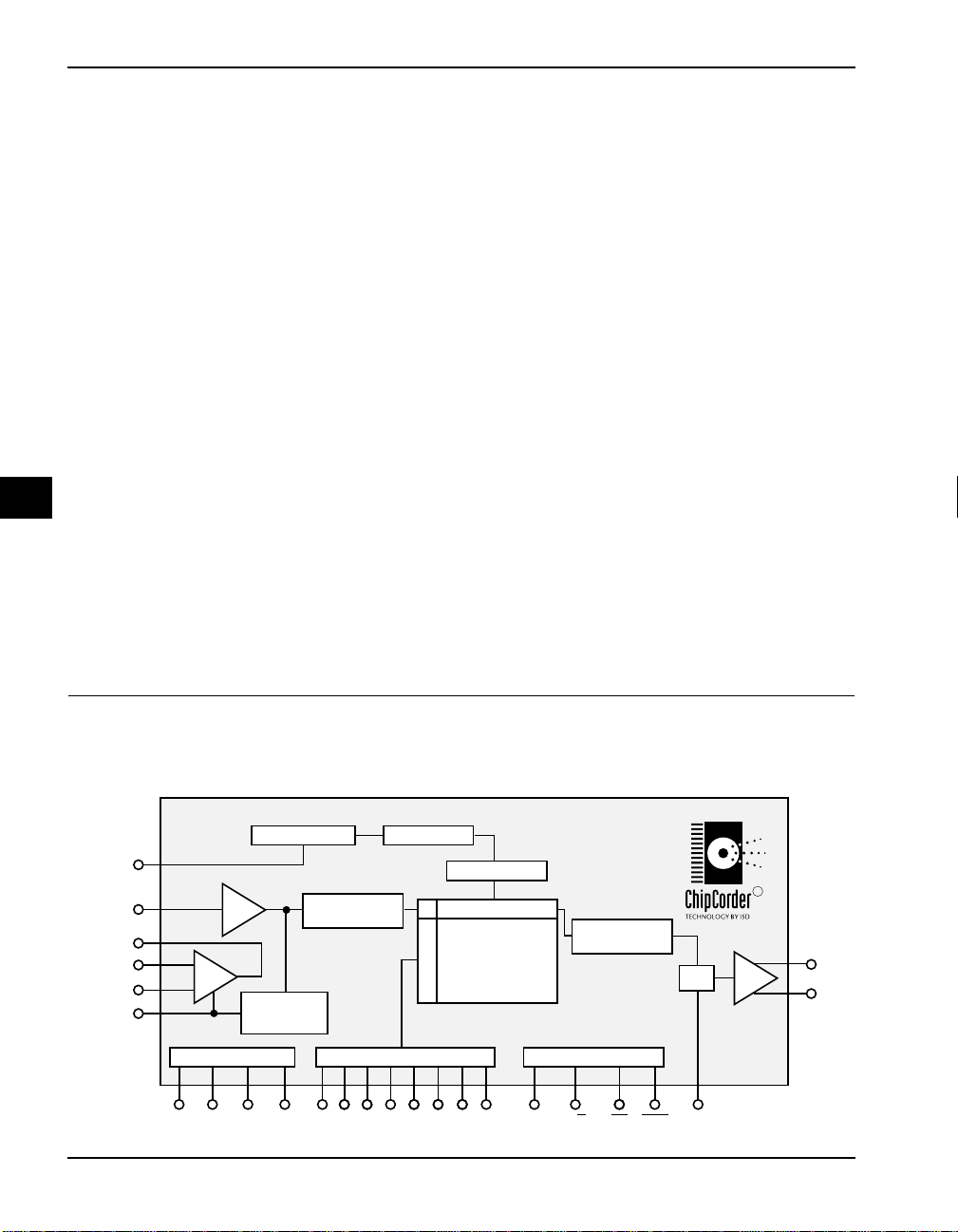
ISD1000A SERIES BLOCK DIAGRAM
Internal Clock
XCLK
ANA IN
ANA OUT
MIC REF
AGC
1–2
MIC
Amp
Pre-
Amp
Power Conditioning
V
V
CCA
SSAVSSD
Automatic
Gain Control
5-Pole Active
Antialiasing Filter
(AGC)
V
CCD
A1
A0 A2 A3 A4 A5 A7A6
Address Buffers
Timing
Sampling Clock
Analog T ransceiv ers
Multilevel Storage
Decoders
128 K Cell
Nonvolatile
Array
5-Pole Active
Smoothing Filter
Device Control
PD P/R CE EOM
Mux
AUX IN
Amp
R
SP+
SP–
Product Data Sheets
ISD1000A Series
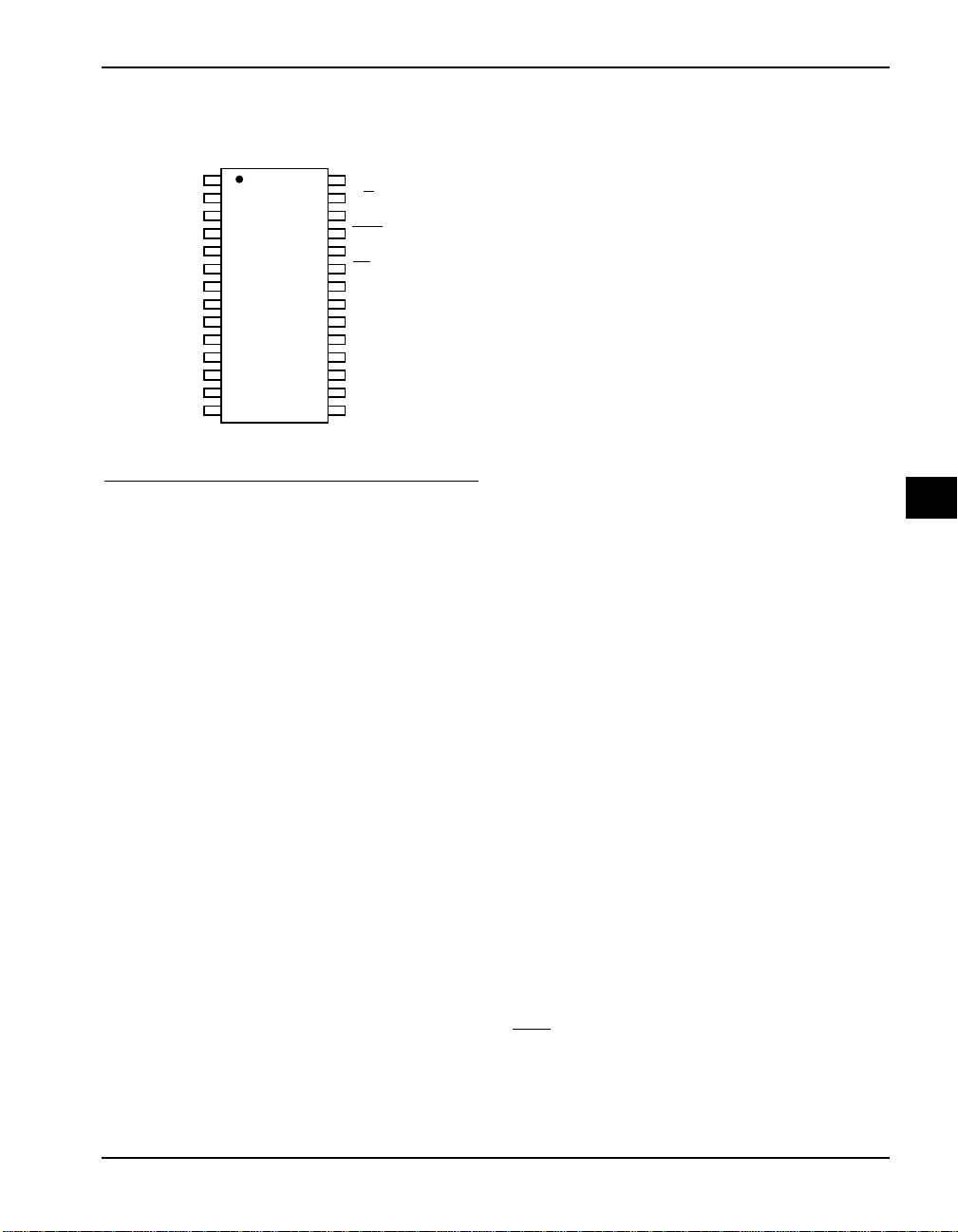
ISD1000A SERIES PINOUTS
28
27
26
25
24
23
22
21
20
19
18
17
16
15
V
CCD
P/R
XCLK
EOM
PD
CE
NC
ANA OUT
ANA IN
AGC
MIC REF
MIC
V
CCA
SP–
NC
NC
SSD
SSA
A6
A7
1
2
3
4
5
6
7
8
9
10
11
12
13
14
DIP/SOIC
M0/A0
M1/A1
M2/A2
M3/A3
M4/A4
M5/A5
AUX IN
V
V
SP+
to achieve longer recording durations. The nonvolatile storage array is based on productionproven, low-power CMOS EEPROM technology.
The highly integrated ISD1000A Series contains
all the basic functions required for high-quality
voice Recording and Playback. The noise-cancelling Microphone Preamplifier and Automatic Gain
Control (AGC) record both low-volume and highvolume sounds. The AGC attack and release
times are adjusted by an external resistor and
capacitor. Antialiasing is performed by a continuous fifth-order Chebyshev filter, requiring no external components or clocks to give toll-quality
reproduction. The low corner of the passband is
user-settable by two external capacitors. The
devices contain their own temperature-stabilized
timebase oscillator.
The ISD1000A devices drive a speaker directly
through differential outputs. This boosts power by
four times and eliminates the need for a series
capacitor or an output amplifier. The device will
operate from a single power supply or from batteries. The device also includes a power down function for applications where minimum power
consumption is critical. The CMOS-based design,
combined with the nonvolatile storage array,
assures the lowest possible overall power consumption.
On-chip control functions make the ISD1000A
Series very easy to use in a wide array of applications. Each device offers a variety of operating
modes and interface options. The devices may be
used in applications that require little more than a
few switches and a battery. The devices may also
be integrated into electronic systems where digital
addresses can be provided for more sophisticated message addressing and control. The
ISD1000A array is organized into 160 segments.
Addresses A0 through A7 provide access to each
segment in the array for message addressing.
Addressing provides the capability of constructing messages by combining stored phrases and
sounds.
PIN DESCRIPTIONS
Voltage Inputs (V
To minimize noise, the analog and digital circuits
in the ISD1000A Series devices use separate
power busses. These voltage busses are brought
out to separate pins and should be tied together
as close to the supply as possible. In addition,
these supplies should be decoupled as close to
the package as possible.
Ground Inputs (V
The ISD1000A Series of devices utilizes separate
analog and digital ground busses. These pins
should be tied together as close to the package
as possible and connected through a low-impedance path to power supply ground.
Power Down Input (PD)
When not recording or playing back, the PD pin
should be pulled HIGH to place the part in a very
low power mode (see I
EOM
pulses LOW for an overflow condition, PD
should be brought HIGH to reset the address
pointer back to the beginning of the Record/Playback space.
CCA
SSA
, V
)
CCD
, V
)
SSD
specification). When
SB
1
1–3

ISD1000A Series
Product Data Sheets
Chip Enable Input (CE
The CE
and Record operations. The address inputs and
Playback/Record input (P/R
falling edge of CE
ISD1000A is unselected, the P/R
auxiliary input is directed into the speaker amplifier.
pin is taken LOW to enable all Playback
Playback/Record Input (P/R
The P/R
CE
while a LOW level selects a Record cycle. For a
Record cycle, the address inputs provide the
starting address and recording continues until PD
or CE
(i.e. the chip is full). When a Record cycle is terminated by pulling PD or CE
-1
sage (EOM) marker is stored at the current
address in memory. For a Playback cycle, the
address inputs provide the starting address and
the device will play until an EOM marker is
encountered. The device can continue past an
EOM marker in an operational mode, or if CE
held LOW in address mode. (See page 1-6 for
more Operational Modes).
input is latched by the falling edge of the
pin. A HIGH level selects a Playback cycle
is pulled HIGH or an overflow is detected
End-Of-Message Output (EOM
A non-volatile marker is automatically inserted at
the end of each recorded message. It remains
there until the message is recorded over. During
Playback, the EOM
period of T
the event of a message overflow (device full).
In addition, the ISD1000A Series has an internal
VCC detect circuit to maintain message integrity
should V
goes LOW and the device is fixed in Playbackonly mode. The EOM marker provides a convenient handshake signal for a processor, and also
facilitates the cascading of devices.
EOM
fall below 3.5V. In this case, EOM
CC
)
) are latched by the
. When CE is taken HIGH, the
is HIGH, and the
)
HIGH, an End-Of-Mes-
)
output pulses LOW for a
at the end of each message, or in
Microphone Input (MIC)
The microphone input transfers its signal to the
on-chip preamplifier. An on-chip Automatic Gain
Control (AGC) circuit controls the gain of this
preamplifier from -15 to 24 dB. An external microphone should be AC coupled to this pin via a
series capacitor. The capacitor value, together
with the internal 10 Kohm resistance on this pin,
determines the low-frequency cutoff for the
ISD1000A Series passband. See ISD’s Application Notes and Design Manual in this book for
additional information on low-frequency cutoff calculation.
Microphone Reference Input (MIC REF)
The MIC REF input is the inverting input to the
microphone preamplifier. This provides a noisecanceling or common-mode rejection input to the
device when connected to a differential microphone.
DISCONNECTED
IF THIS INPUT IS UNUSED, IT MUST BE LEFT
.
Automatic Gain Control Input (AGC)
is
The AGC dynamically adjusts the gain of the
preamplifier to compensate for the wide range of
microphone input levels. The AGC allows the full
range of whispers to loud sounds to be recorded
with minimal distortion. The “attack” time is determined by the time constant of a 5 KΩ internal
resistance and an external capacitor (C2) connected from the AGC pin to V
The “release” time is determined by the time constant of an external resistor (R2) and an external
capacitor (C2 on the schematic on page 1-17)
connected in parallel between the AGC Pin and
V
analog ground. Nominal values of 470 K
SSA
and 4.7 µF give satisfactory results, in most cases.
For AGC voltages of 1.5V and below, the preamplifier is at its maximum gain of 24 dB. Reduction
in preamplifier gain occurs for voltages of approximately 1.8V.
analog ground.
SSA
Ω
1–4
Product Data Sheets
ISD1000A Series
Analog Output (ANA OUT)
This pin provides the preamplifier output to the
user. The voltage gain of the preamplifier is determined by the voltage level at the AGC pin. It has a
maximum gain of about 24 dB for small input signal levels.
Analog Input (ANA IN)
The analog input pin transfers its signal to the chip
for recording. For microphone inputs, the ANA
OUT pin should be connected via an external
capacitor to the ANA IN pin. This capacitor value,
together with the 2.7 KΩ input impedance of ANA
IN, is selected to give additional cutoff at the lowfrequency end of the voice passband. If the
desired input is derived from a source other than
a microphone, the signal can be fed, capacitively
coupled, into the ANA IN pin directly.
Optional External Clock Input (XCLK)
ISD1000A devices are configured at the factory
with an internal sampling clock frequency centered to ±1% of specification. The frequency is
maintained to a total variation of ±2.25% tolerance over the entire commercial temperature and
4.5 to 5.5 voltage ranges. The internal clock has a
±
5% tolerance over the industrial temperature
range and 4.5 to 5.5 voltage range. A regulated
power supply is recommended for industrial-temperature-range parts. If greater precision is
required, the device can be clocked through the
XCLK pin as follows.
Part
Number
ISD1016A 8.0 KHz 1024 KHz
ISD1020A 6.4 KHz 819.2 KHz
These recommended clock rates should not be
varied because the antialiasing and smoothing filters are fixed, and aliasing problems can occur if
the sample rate differs from the one recommended. The duty cycle on the input clock is not
Sample Rate Required Clock
critical, as the clock is immediately divided by
two.
IF THE XCLK IS NOT USED, THIS INPUT MUST BE
CONNECTED
TO
GROUND
.
Speaker Outputs (SP+/SP-)
All devices in the ISD1000A Series include an onchip differential speaker driver, capable of driving
50 milliwatts into 16 Ω from AUX IN (12.2 mW from
memory).
The speaker outputs are held at V
record and power down. It is therefore not possible to parallel speaker outputs of multiple
ISD1000A devices or the outputs of other speaker
drivers.
NOTE
levels during
SSA
Connection of speaker outputs in parallel
may cause damage to the device.
While a single output may be used alone (including a coupling capacitor between the SP pin and
the speaker), these outputs may be used individually with the output signal taken from either pin.
Using the differential outputs results in a 4:1
improvement in output power.
NOTE
Never ground or drive an output.
Auxiliary Input (AUX IN)
The Auxiliary Input is multiplexed through to the
output amplifier and speaker output pins when CE
is HIGH and Playback has ended, or if the device
is in overflow. When cascading multiple ISD1000A
devices, the AUX IN pin is used to connect a Playback signal from a following device to the
previous output speaker drivers. For noise considerations, it is suggested that the Auxiliary Input not
be driven when the storage array is active.
Address/Mode Inputs (Ax/Mx)
The Address/Mode Inputs provide two functions in
the ISD1000A Series: 1. Message address (either
1
1–5

ISD1000A Series
Product Data Sheets
A6 or A7 = LOW) and 2. ISD1000A Series Operational Mode Options (A6 AND A7 = HIGH).
Operational mode options are shown in the Operational Modes table. There are a maximum of 160
message addresses (or segments). Each segment corresponds to one of 160 rows in the analog storage array. The message addresses
(segments) are in locations 0 through 159 contiguous. The playback/record duration of each segment depends upon the device and is as follows:
Part
Number
ISD1016A 100 milliseconds
ISD1020A 125 milliseconds
Segment Playback/Record
Duration
-1
An operation may be started at any address, as
defined by address pins A0-A7. Record or playback continues with automatic incrementing of the
internal on-chip address until either CE
HIGH (Record), an end of message marker is
encountered (Playback with CE
flow (device full) condition results.
HIGH), or an over-
is brought
OPERATIONAL MODES
The ISD1000A Series is designed with several
built-in operational modes provided to allow maximum functionality with a minimum of additional
components, described in detail below. The operational modes use the address pins on the
ISD1000A devices, but are mapped outside the
valid address range. When the two Most Significant Bits (MSBs) are HIGH (A6 = A7=1), the
remaining address signals are interpreted as
mode bits and
operational modes and direct addressing are not
compatible and cannot be used simultaneously.
There are two important considerations for using
operational modes. First, all operations begin initially at address 0, which is the beginning of the
ISD1000A address space. Later operations can
begin at other address locations, depending on
the operational mode(s) chosen. In addition, the
address pointer is reset to 0 when the device is
changed from Record to Playback, or when a
Power-Down cycle is executed.
Second, an Operational Mode is executed when
CE
goes LOW and the two MSBs are HIGH. This
Operational Mode remains in effect until the next
NOT
as address bits. Therefore,
OPERATIONAL MODES TABLE
Control
Mode
M0 Message cueing Fast-forward through messages M4, M5
M1 Delete EOM markers Position EOM marker at the end of the last
M2 Cascading Adding devices to extend message
M3 Looping Continuous playback from Address 0 M1, M5
M4 Consecutive addressing Record/Play multiple consecutive mes-
M5 CE level-activated Allow message pausing M0, M1, M3, M4
NOTE:
An asterisk (*) indicates additional operational modes which can be used simultaneously with the given mode.
1–6
Function Typical Use Jointly Compatible*
M3, M4, M5
message
M0, M1, M5
sages
 Loading...