

Page 1
Tel: (800) 404-0204
www.ironwoodelectronics.com
Kelvin Testing Using a GHz socket for MLF/QFN packages
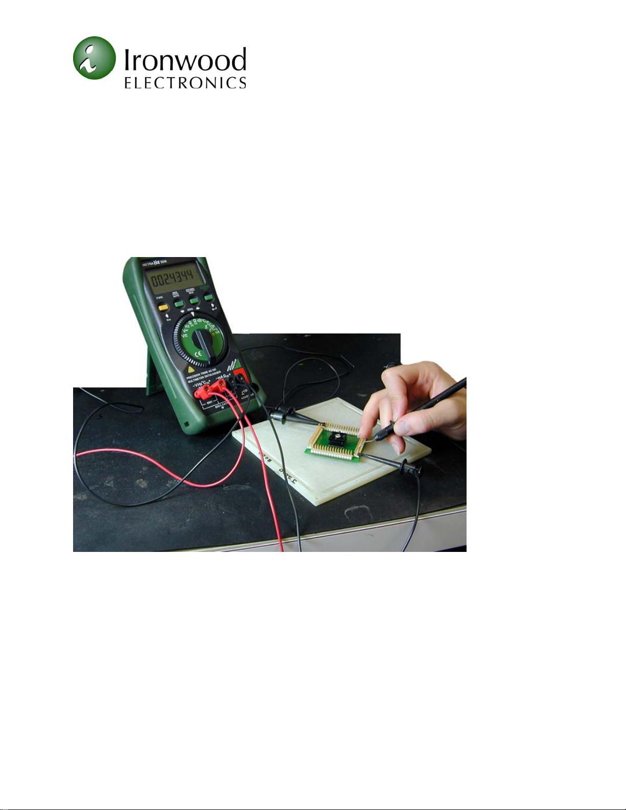
A measurement method called Kelvin probing for measuring resistance allows very accurate
measurement of milliohm or sub-milliohm resistance. To accomplish this there are two
leads, which provide a current source across the load to be measured, and two more leads
across the load, which provide the sensing. This is shown in Fig. 1. The problem is that it
takes twice as many connections as with a two-wire measurement. There is no lead
resistance in the measurement as there is of course with the two-wire measurement. This can
easily be several tenths of an OHM, thus swamping out the milliohms that are to be
measured.
Figure 1: Test Setup.
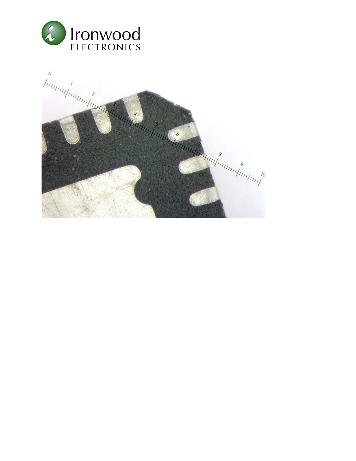
A further complication arises when accurate measurements are required in very small
packages. Many analog functions are being packaged in MLF/QFN packages. These
devices have pitches as low as 0.4mm and lead dimensions in the range of 0.5mm x 0.25mm.
A bottom view of an MLF/QFN package is shown in Fig. 2.
Page 2
Tel: (800) 404-0204
www.ironwoodelectronics.com
Figure 2: MLF pad detail
Ironwood Electronics, Inc. has developed a socket for MLF device, which has two features
that allow the socket to be used for Kelvin probing in an MLF device. The first feature of the
socket is that it has a very high density contactor which consists of tiny gold plated wires
spaced 0.05mm apart or two thousandths of an inch mounted at a slight angle from vertical in
an elastomer material. This sea of wires provides the connection between two parallel
conductors forced together such as the lead on an MLF and a pad on a PCB with the
contactor between. The second feature is a patent pending method for precisely positioning
the MLF/QFN leads precisely over the pads on the target PCB. This socket was originally
designed as a 10 GHz bandwidth socket for testing very high frequency circuits in MLF/QFN
packages.
To use the GHz MLF socket as a Kelvin measurement device, the target board has to be
designed as shown in Figure 3. Figure 3A shows the layout for use as a standard socket.
Figure 3B shows the layout for use as a Kelvin measurement socket. The difference is that
the pads for Figure 3B are split in the center and a gap of 0.125mm are inserted between the
two sections of the pad. Each fragmentary section of the standard pad or two smaller pads is
then connected to the measuring circuitry as shown in the figure. The current source is
connected to one section of the pad and the sensing circuit is connected to the other section
Page 3

of the bisected pad.
Tel: (800) 404-0204
www.ironwoodelectronics.com
15.225mm
Socket size
Orientation Mark
±0.125mm sqr.
1.25mm
9.36mm
±0.13mm (x4)
1.68mm
7.78mm
5.08mm
12.725mm
1.25mm
MLF64A
±0.125mm (x4)
2.72mm*
7.78mm
9.36mm
±0.125mm (x4)
Figure 3A: Suggested PCB layout for SG-MLF-7008
0.5mm typ.
2.54mm
+
Ø 0.85mm
0.025mm
-
0.025mm
Non plated alignment hole
0.69 x 0.28 mm
Ø 1.61mm
+
-
Non plated mounting hole
(x 2 )
pad (x 64)
0.050mm
0.050mm
(x 4)
Figure 3B: Split pad layout
For our purposes, an SG-MLF-7008 was used with a 64-position MLF test chip. The chip
was set up in a daisy chain pattern and provides a resistance through spiral circuitry from
bottom to top of board (Figure 4). The target board allows Kelvin connections to every pin.
The results are shown below in Fig. 5.
Page 4

Tel: (800) 404-0204
www.ironwoodelectronics.com
Figure 4: Test Chip layout
The MLF GHz sockets vary by package; call Ironwood Electronics, Inc. for assistance in
choosing the proper socket before laying out your board. Tooling holes, etc must be in the
correct locations to ensure the best test set-up. If needed, Ironwood Electronics, Inc. can also
provide a board for Kelvin testing. Call for a quote.
Figure 5: Test Data
Leads Resistance
1:2 2.3543 1:20 2.4028 1:38 2.3932 1:56 2.3499
Page 5

Tel: (800) 404-0204
www.ironwoodelectronics.com
1:3 0.0112 1:21. 0.0483 1:39 0.0844 1:57 0.026
1:4 2.3584 1:22 2.409 1:40 2.418 1:58 2.3544
1:5 0.0155 1:23 0.0512 1:41 0.0865 1:59 0.023
1:6 2.3672 1:24 2.4156 1:42 2.4094 1:60 2.3637
1:7 0.0211 1:25 0.0555 1:43 0.0913 1:61 0.019
1:8 2.3754 1:26 2.4228 1:44 2.434 1:62 2.3701
1:9 0.0246 1:27 0.0601 1:45 0.0954 1:63 0.0163
1:10 2.3853 1:28 2.4308 1:46 2.4269 1:64 2.3753
1:11 0.0294 1:29 0.0643 1:47 0.1055
1:12 2.3943 1:30 2.4381 1:48 2.4349
1:13 0.0331 1:31 0.0686 1:49 0.045
1:14 2.3984 1:32 2.4463 1:50 2.3341
1:15 0.0365 1:33 0.0712 1:51 0.0407
1:16 2.3944 1:34 2.3822 1:52 2.3402
1:17 0.0388 1:35 0.0752 1:53 0.0351
1:18 2.3933 1:36 2.3917 1:54 2.3457
1:19 0.0444 1:37 0.0812 1:55 0.0305
Conclusion: From the results in Figure 5, one can ascertain that using the GHz socket in
the described setup can in fact measure the Kelvin resistance between two points. The
test chip that was daisy chained in this pattern allowed us to see differences between
points because of the length of the trace (more length = more resistance), you can see that
the farther you got away from the first pin, the resistance increases slightly. It was used
expressly for that purpose; a typical MLF chip will also work in this application although
the results will be unique to that chip.
 Loading...