

IRF IRU1160CM, IRU1160CP Schematics
Data Sheet No. PD94130
IRU1160
6A ULTRA LOW DROPOUT POSITIVE
ADJUSTABLE REGULATOR
FEATURES
0.62V Dropout at 6A
Fast Transient Response
1% Voltage Reference Initial Accuracy
Built-In Thermal Shutdown
APPLICATIONS
VGA Card Applications
On-Board Low Voltage Regulator Supply such
as 3.3V to 2.8V
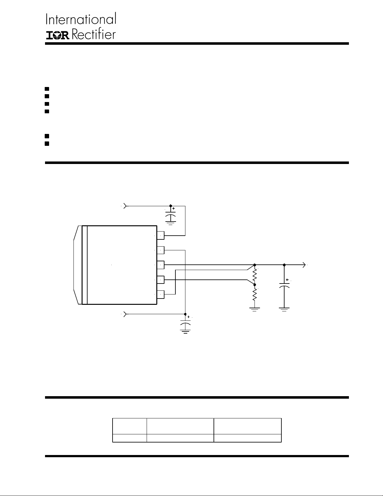
TYPICAL APPLICATION
3.3V
100uF
V
IN
V
CTRL
DESCRIPTION
The IRU1160 is a 6A regulator with extremely low dropout voltage using a proprietary bipolar process that
achieves comparable equivalent on resistance to that of
discrete MOSFETs. This product is specifically designed
to provide well regulated supply for applications requiring 2.8V or lower voltages from 3.3V ATX power supplies
where high efficiency of a switcher can be achieved without the cost and complexity associated with switching
regulators.
C1
5
4
V
OUT
Adj
SENSE
3
2
1
C2
100uF
IRU1160
V
5V
Figure 1 - Typical application of IRU1160 in a 3.3V to 2.8V.
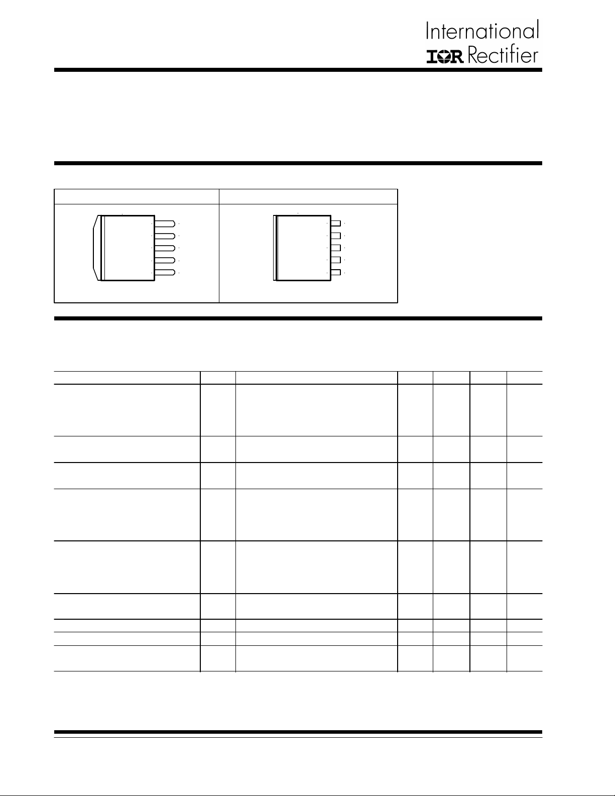
PACKAGE ORDER INFORMATION
TJ (°C) 5-PIN PLASTIC 5-PIN PLASTIC
TO-263 (M) Ultra Thin-PakTM (P)
0 To 125 IRU1160CM IRU1160CP
R1
100
1%
R2
124
1%
2.7V
C3
100uF
Rev. 1.4
08/20/02
www.irf.com
1
IRU1160
ABSOLUTE MAXIMUM RATINGS
Input Voltage (V IN) .................................................... 7V
Control Input Voltage (V CTRL) ..................................... 14V
Power Dissipation ..................................................... Internally Limited
Storage Temperature Range ...................................... -65°C To 150°C
Operating Junction Temperature Range ..................... 0°C To 150°C
PACKAGE INFORMATION
V
IN
V
CTRL
V
OUT
Adj
V
SENSE
TM
(P)
1.225
1.225
6.2
60
1.250
1.250
1.00
1.10
1.20
0.15
0.40
0.55
5
0.01
70
1.275
1.275
3
6
1.30
0.20
0.52
0.62
10
0.02
V
mV
mV
V
V
A
mA
%/W
dB
5-PIN PLASTIC TO-263 (M) 5-PIN PLASTIC ULTRA THIN-PAK
Tab is
VOUT
FRONT VIEW
5
4
3
2
1
V
IN
V
CTRL
V
OUT
Adj
V
SENSE
Tab is
VOUT
FRONT VIEW
5
4
3
2
1
θJA=35°C/W for 0.5" square pad θJA=35°C/W for 0.5" square pad
ELECTRICAL SPECIFICATIONS
Unless otherwise specified, these specifications apply over CIN=mF, COUT=10mF, and TJ=0 to 1258C.
Typical values refer to TJ=258C. VOUT=VSENSE.
PARAMETER SYM TEST CONDITION MIN TYP MAX UNITS
Reference Voltage
Line Regulation
Load Regulation (Note 1)
Dropout Voltage (Note 2)
(VCTRL - VOUT)
Dropout Voltage (Note 2)
(VIN - VOUT)
Current Limit
Minimum Load Current (Note 3)
Thermal Regulation
Ripple Rejection
VREF
VCTRL=2.75, V IN=2V, Io=10mA,
TJ=258C, VADJ=0V
VCTRL=2.7 to 12V, V IN=2.05V to 5.5V,
Io=10mA to 6A, VADJ=0V
VCTRL=2.5V to 7V, V IN=1.75V to 5.5V,
Io=10mA, VADJ=0V
VCTRL=2.75V, VIN=2.1V,
Io=10mA to 6A, VADJ=0V
VADJ=0V for all conditions below:
VIN=2.05V, Io=1.5A
VIN=2.05V, Io=5A
VIN=2.05V, Io=6A
VADJ=0V for all conditions below:
VCTRL=2.75V, Io=1.5A
VCTRL=2.75V, Io=5A
VCTRL=2.75V, Io=6A
VCTRL=2.75V, VIN=2.05V,
DVo=100mV, VADJ=0V
VCTRL=5V, VIN=3.3V, VADJ=0V
30ms Pulse
VCTRL=5V, VIN=5V, Io=5A, VADJ=0V,
TJ=258C, VRIPPLE=1VPP at 120Hz
2
www.irf.com
Rev. 1.4
08/20/02
IRU1160
PARAMETER SYM TEST CONDITION MIN TYP MAX UNITS
Control Pin Current
Adjust Pin Current
VADJ=0V for all below conditions:
VCTRL=2.75V, VIN=2.05V, Io=1.5A
VCTRL=2.75V, VIN=2.05V, Io=5A
VCTRL=2.75V, VIN=2.05V, Io=6A
VCTRL=2.75V, VIN=2.05V, VADJ=0V
15
50
60
50 120
mA
mAIADJ
Note 1: Low duty cycle pulse testing with Kelvin connections are required in order to maintain accurate data.
Note 2: Dropout voltage is defined as the minimum differential between VIN and VOUT required to maintain regulation at VOUT. It is measured when the output voltage
drops 1% below its nominal value.
PIN DESCRIPTIONS
PIN # PIN SYMBOL PIN DESCRIPTION
1
2
3
4
5
VSENSE
Adj
VOUT
VCTRL
VIN
This pin is the positive side of the reference which allows remote load sensing to achieve
excellent load regulation.
A resistor divider from this pin to the VOUT pin and ground sets the output voltage.
The output of the regulator. A minimum of 10mF capacitor must be connected from this
pin to ground to insure stability.
This pin is the supply pin for the internal control circuitry as well as the base drive for the
pass transistor. This pin must always be higher than the VOUT pin in order for the device to
regulate. (See specifications)
The input pin of the regulator. Typically a large storage capacitor is connected from this
pin to ground to insure that the input voltage does not sag below the minimum dropout
voltage during the load transient response. This pin must always be higher than VOUT in
order for the device to regulate. (See specifications)
Note 3: Minimum load current is defined as the minimum current required at the output in order for the output voltage to maintain regulation. Typically the resistor
dividers are selected such that it automatically maintains this current.
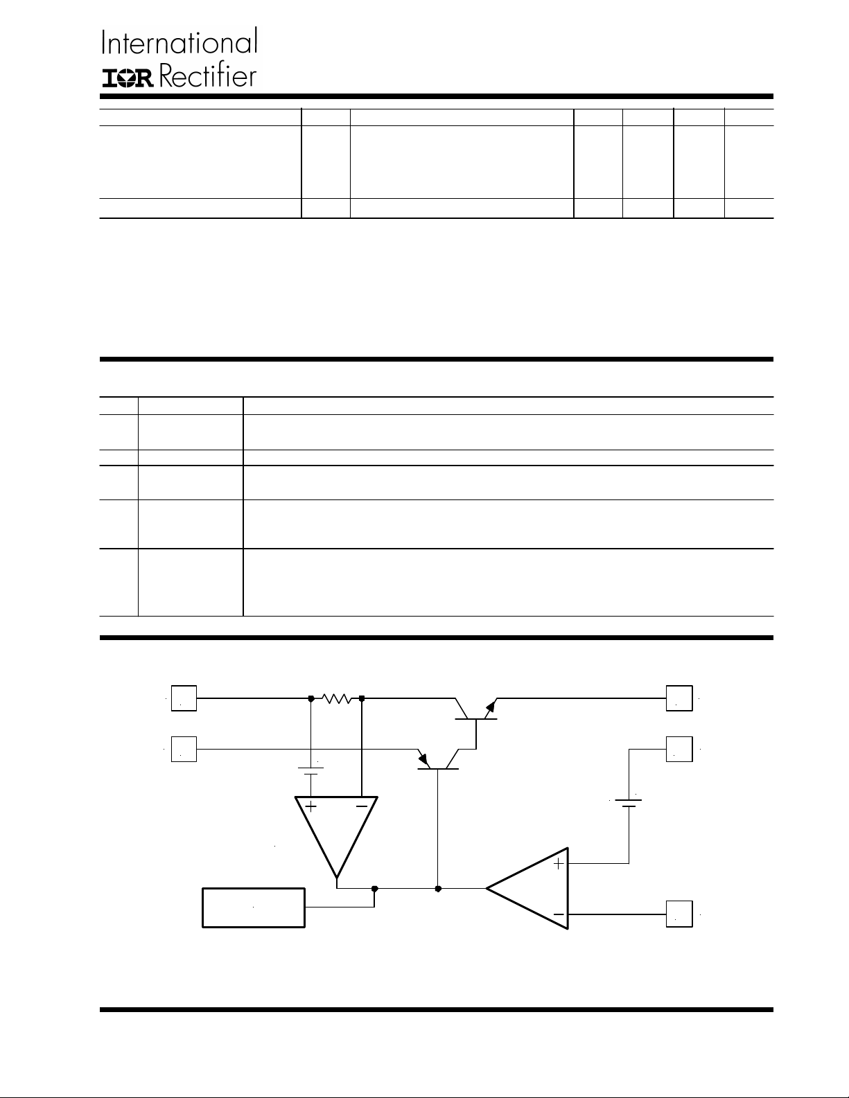
BLOCK DIAGRAM
V
IN
5
V
CTRL
Rev. 1.4
08/20/02
4
CURRENT
LIMIT
THERMAL
SHUTDOWN
+
1.25V
Figure 2 - Simplified block diagram of the IRU1160.
www.irf.com
V
OUT
3
V
SENSE
1
+
2
Adj
3
 Loading...