

IRF IRS44273LPBF Schematic [ru]
IRS44273LPBF
1
www.irf.com
© 2015 International Rectifier
January 15, 2015
Features
CMOS Schmitt-triggered inputs
Under voltage lockout
3.3V logic compatible
Output in phase with input
Leadfree, RoHS compliant
Typical Applications
General Purpose Gate Driver
DC-DC converters
Plasma display panel (PDP) applications
Product Summary
Topology
General Driver
Io+ & I
o-
(typical)
1.5A / 1.5A
ton & t
off
(typical)
50ns & 50ns
Package Type
5 Lead SOT23
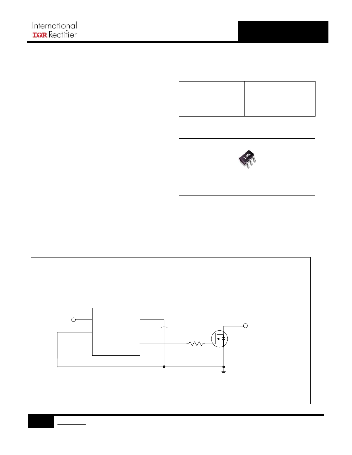
Typical Connection Diagram
IN
OUT
VCC
IRS44273L
OUT
COM
IN
HVIC
TM
Single Low-Side Driver IC
IRS44273L
2
www.irf.com
© 2015 International Rectifier
January 15, 2015
Table of Contents
Page
Typical connection diagram
1
Description
3
Qualification Information
4
Absolute Maximum Ratings
5
Recommended Operating Conditions
5
Static Electrical Characteristics
6
Dynamic Electrical Characteristics
6
Functional Block Diagrams
7
Input/Output Pin Equivalent Circuit Diagram
8
Lead Definitions
9
Lead Assignments
9
Application Information and Additional Details
10
Package Details: SOT23-5
11
Package Details: SOT23-5, Tape and Reel
12
Part Marking Information
14
Ordering Information
15

IRS44273L
3
www.irf.com
© 2015 International Rectifier
January 15, 2015
Description
The IRS44273L is a low voltage, power MOSFET and IGBT non-inverting gate driver. Proprietary latch immune
CMOS technologies enable ruggedized monolithic construction. The logic input is compatible with standard
CMOS or LSTTL output. The output driver features a current buffer stage.
IRS44273L
4
www.irf.com
© 2015 International Rectifier
January 15, 2015
Qualification Level
Industrial††
Comments: This family of ICs has passed JEDEC’s
Industrial qualification. IR’s Consumer qualification level is
granted by extension of the higher Industrial level.
Moisture Sensitivity Level
MSL1
†††
260°C
(per IPC/JEDEC J-STD-020)
ESD
Machine Model
Class B
(per JEDEC standard JESD22-A115)
Human Body Model
Class 2
(per EIA/JEDEC standard EIA/JESD22-A114)
IC Latch-Up Test
Class 1 Level A
(per JESD78)
RoHS Compliant
Yes
†
Qualification standards can be found at International Rectifier’s web site http://www.irf.com/
††
Higher qualification ratings may be available should the user have such requirements. Please contact your
International Rectifier sales representative for further information.
†††
Higher MSL ratings may be available for the specific package types listed here. Please contact your
International Rectifier sales representative for further information.
Qualification Information†
IRS44273L
5
www.irf.com
© 2015 International Rectifier
January 15, 2015
VCC
Fixed supply voltage
-0.3
25
V
VO
Output voltage
-0.3
V
CC
+ 0.3
VIN
Logic input voltage
-0.3
V
CC
+ 0.3
PD
Package power dissipation @ TA ≤ 25°C
—
250
mW
RthJA
Thermal resistance, junction to ambient
—
191
°C/W
TJ
Junction temperature
—
150
°C
TS
Storage temperature
-55
150
TL
Lead temperature (soldering, 10 seconds)
—
300
Symbol
Definition
Min
Max
Units
Symbol
Definition
Min
Max
Units
VCC
Fixed supply voltage
---
20 V VO
Output voltage
0
VCC
VIN
Logic input voltage
0
VCC
TA
Ambient temperature
-40
125
°C
Absolute Maximum Ratings
Absolute maximum ratings indicate sustained limits beyond which damage to the device may occur. The device
may not function or not be operable above the recommended operating conditions and stressing the parts to
these levels is not recommended. In addition, extended exposure to stresses above the recommended operating
conditions may affect device reliability. All voltage parameters are absolute voltages referenced to COM. The
thermal resistance and power dissipation ratings are measured under board mounted and still air conditions.
Recommended Operating Conditions
For proper operation, the device should be used within the recommended conditions. All voltage parameters are
absolute voltages referenced to COM unless otherwise stated in the table. The offset rating is tested with supply
of VCC = 15V.
 Loading...