

IRF IRS2541STRPbF, IRS2540 Datasheet
www.irf.com Page 1
Data Sheet No. PD60293
IRS254(0,1)(S)PbF
LED BUCK REGULATOR CONTROL IC
Description
The IRS254(0,1) are high voltage, high frequency
buck control ICs for constant LED current regulation.
They incorporate a continuous mode time-delayed
hysteretic buck regulator to directly control the
average load current, using an accurate on-chip
bandgap voltage reference.
The application is inherently protected against short
circuit conditions, with the ability to easily add opencircuit protection. An external high-side bootstrap
circuit drives the buck switching element at high
frequencies. A low-side driver is also provided for
synchronous rectifier designs. All functions are
realized within a simple 8 pin DIP or SOIC package.
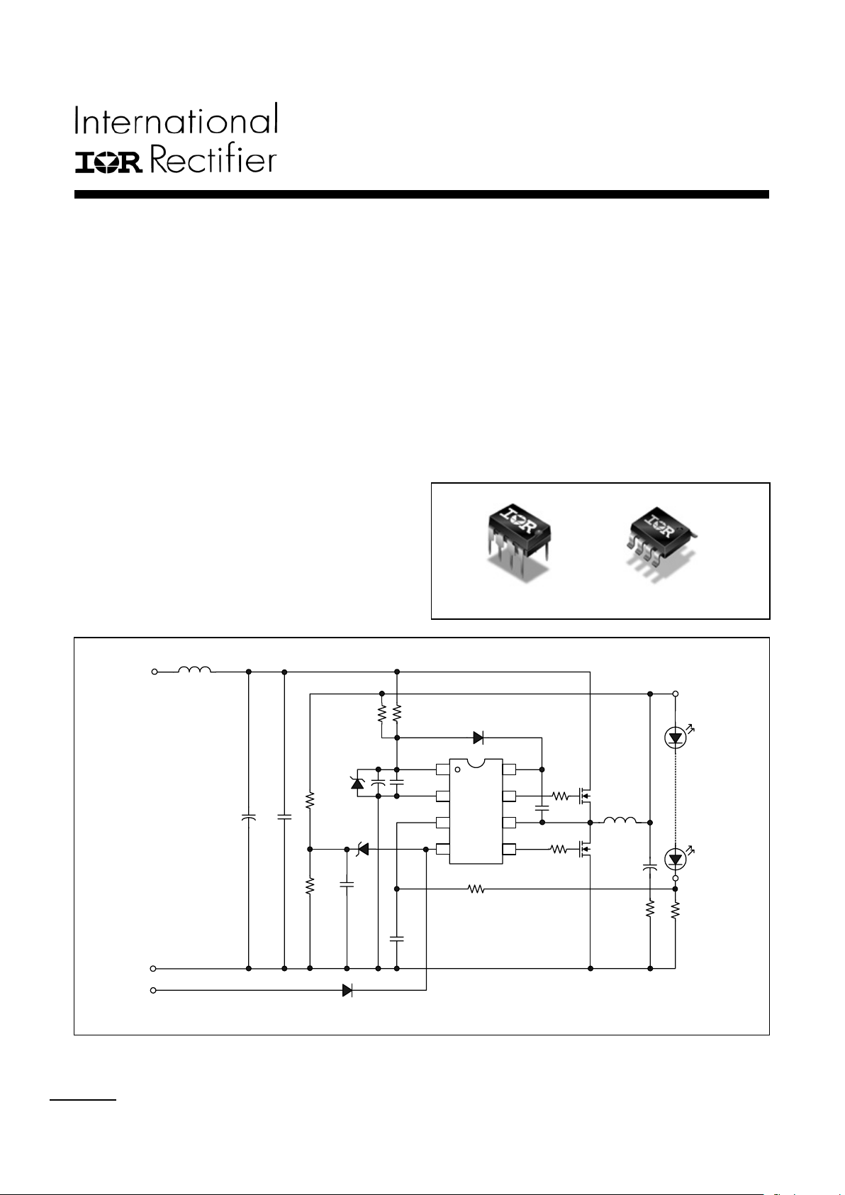
Typical Application Diagram
Features
• 200 V (IRS2540) and 600 V (IRS2541) half bridge
driver
• Micropower startup (<500 µA)
• ±2% voltage reference
• 140 ns deadtime
• 15.6 V zener clamp on V
CC
• Frequency up to 500 kHz
• Auto restart, non-latched shutdown
• PWM dimmable
• Small 8-Lead DIP/8-Lead SOIC packages
Packages
8-Lead PDIP 8-LeadSOIC
IRS254(0,1)PbF IRS254(0,1)SPbF
1
2
3
4
8
7
6
5
IRS254(0,1)
VCC
IFB
LO
VS
HO
VB
COM
M1
M2
CBOOT
DBOOT
RCS
RF
CF
RS1
CVCC1
CVCC2
ROV1
ROV2
CEN
DOV
DEN1
L1
EN
COM
VBUS
COUT
RG1
RG2
VOUT+
VOUT-
IC1
CBUS2
RS2
DCLAMP
CBUS1
L2
ENN
ROUT

IRS254(0,1)(S)PbF
www.irf.com Page 2
Alternate application circuit using a single MOSFET
IRS254(0,1)
IRS254(0,1)(S)PbF
www.irf.com Page 3
Absolute Maximum Ratings
Absolute maximum ratings indicate sustained limits beyond which damage to the device may occur. All voltage
parameters are absolute voltages referenced to COM, all currents are defined positive into any lead. The thermal
resistance and power dissipation ratings are measured under board mounted and still air conditions.
Symbol Definition Min. Max. Units
IRS2540 -0.3 225
VB High-side floating supply voltage
IRS2541 -0.3 625
VS High-side floating supply offset voltage VB – 25 VB + 0.3
VHO High-side floating output voltage VS – 0.3 VB + 0.3
VLO Low-side output voltage -0.3 VCC + 0.3
V
IFB
Feedback voltage -0.3 VCC + 0.3
V
ENN
Enable voltage -0.3 VCC + 0.3
V
ICC Supply current (Note 1) -20 20 mA
dV/dt Allowable offset voltage slew rate -50 50 V/ns
(8-Pin DIP) --- 1
PD
Package power dissipation @ T
A
≤ +25 ºC
P
D
= (T
JMAX-TA
)/R
THJA
(8-Pin SOIC) --- 0.625
W
(8-Pin DIP) --- 125
R
THJA
Thermal resistance, junction to ambient
(8-Pin SOIC) --- 200
ºC/W
TJ Junction temperature -55 150
TS Storage temperature -55 150
TL Lead temperature (soldering, 10 seconds) --- 300
ºC
Note 1: This IC contains a zener clamp structure between the chip V
CC
and COM, with a nominal breakdown voltage of
15.6 V. Please note that this supply pin should not be driven by a low impedance DC power source greater than V
CLAMP
specified in the electrical characteristics section.
Recommended Operating Conditions
For proper operation the device should be used within recommended conditions.
Symbol Definition Min. Max. Units
VBS High side floating supply voltage VCC – 0.7 V
CLAMP
IRS2540
-1 200
VS
Steady state high-side floating supply offset voltage
IRS2541 -1 600
VCC Supply voltage V
CCUV+
V
CLAMP
V
ICC Supply current Note 2 10 mA
TJ Junction temperature -25 125 ºC
Note 2: Sufficient current should be supplied to
V
CC
to keep the internal 15.6 V zener regulating at V
CLAMP
.
IRS254(0,1)(S)PbF
www.irf.com Page 4
Electrical Characteristics
VCC = VBS = V
BIAS
= 14 V +/- 0.25 V, CLO=CHO=1000 pF, C
VCC=CVBS
=0.1 µF, TA=25 °C unless otherwise specified.
Symbol Definition Min Typ Max Units Test Conditions
Supply Characteristics
V
CCUV+
VCC supply undervoltage positive going
threshold
8.0 9.0 10.0 VCC rising from 0 V
V
CCUV-
VCC supply undervoltage negative going
threshold
6.5 7.5 8.5 VCC falling from 14 V
V
UVHYS
VCC supply undervoltage lockout hysteresis 1.0 1.2 2.0
V
I
QCCUV
UVLO mode quiescent current --- 50 150 µA VCC=6 V
I
QCCENN
Diesabled mode quiescent current --- 1.0 2.0 EN>V
ENTH+
I
QCC
Quiescent VCC supply current --- 1.0 2.0 IFB = 1 V
I
CC50k
VCC supply current, f = 50 kHz --- 2.0 3.0
mA
Duty Cycle = 50%
f = 50 kHz
V
CLAMP
VCC zener clamp voltage 14.6 15.6 16.6 V ICC = 10 mA
Floating Supply Characteristics
I
QBS0
Quiescent VBS supply current --- 1.0 2.0 VHO = VS
I
QBS1
Quiescent VBS supply current --- 2.0 3.0
mA
IFB = 0 V
V
BSUV+
VBS supply undervoltage positive going
threshold
6.5 7.5 8.5
V
BSUV-
VBS supply undervoltage negative going
threshold
6.0 7.0 8.0
V
ILK Offset supply leakage current --- 1 50 µA
IRS2540:VB=VS=200 V
IRS2541:VB=VS=600 V
Current Control Operation
V
ENNTH+
ENN pin positive threshold 2.5 2.7 3.0
V
ENNTH-
ENN pin negative threshold 1.7 2.0 2.3
V
V
0.5
0.5 V voltage reference (die level test) 490 500 510
V
IFBTH
IFB pin threshold 455 500 540
mV
f Maximum frequency --- 500 --- kHz
Gate Driver Output Characteristics
VOL Low level output voltage (HO or LO) --- COM ---
VHL High level output voltage (HO or LO) --- VCC ---
V
tr Turn-on rise time --- 50 120
tf Turn-off fall time --- 30 50
ns
I
O+/-
Output source/sink short circuit pulsed current --- 0.5/0.7 --- A
DT Deadtime --- 140 ---
t
LO,ON
Delay between V
IFB>VIFBTH
and LO turn-on --- 320 ---
t
LO,OFF
Delay between V
IFB<VIFBTH
and LO turn-off --- 180 ---
t
HO,ON
Delay between V
IFB<VIFBTH
and HO turn-on --- 320 ---
t
HO,OFF
Delay between V
IFB>VIFBTH
and HO turn-off --- 180 ---
ns
IFB = 50 kHz square
wave, 200 mV pk-pk
DC offset = 400 mV
Duty Cycle = 50%
IRS254(0,1)(S)PbF
www.irf.com Page 5
Electrical Characteristics
V
CC
= VBS = V
BIAS
= 14 V +/- 0.25 V, CLO=CHO=1000 pF, C
VCC=CVBS
=0.1 µF, TA=25 °C unless otherwise specified.
Symbol Definition Min Typ Max Units Test Conditions
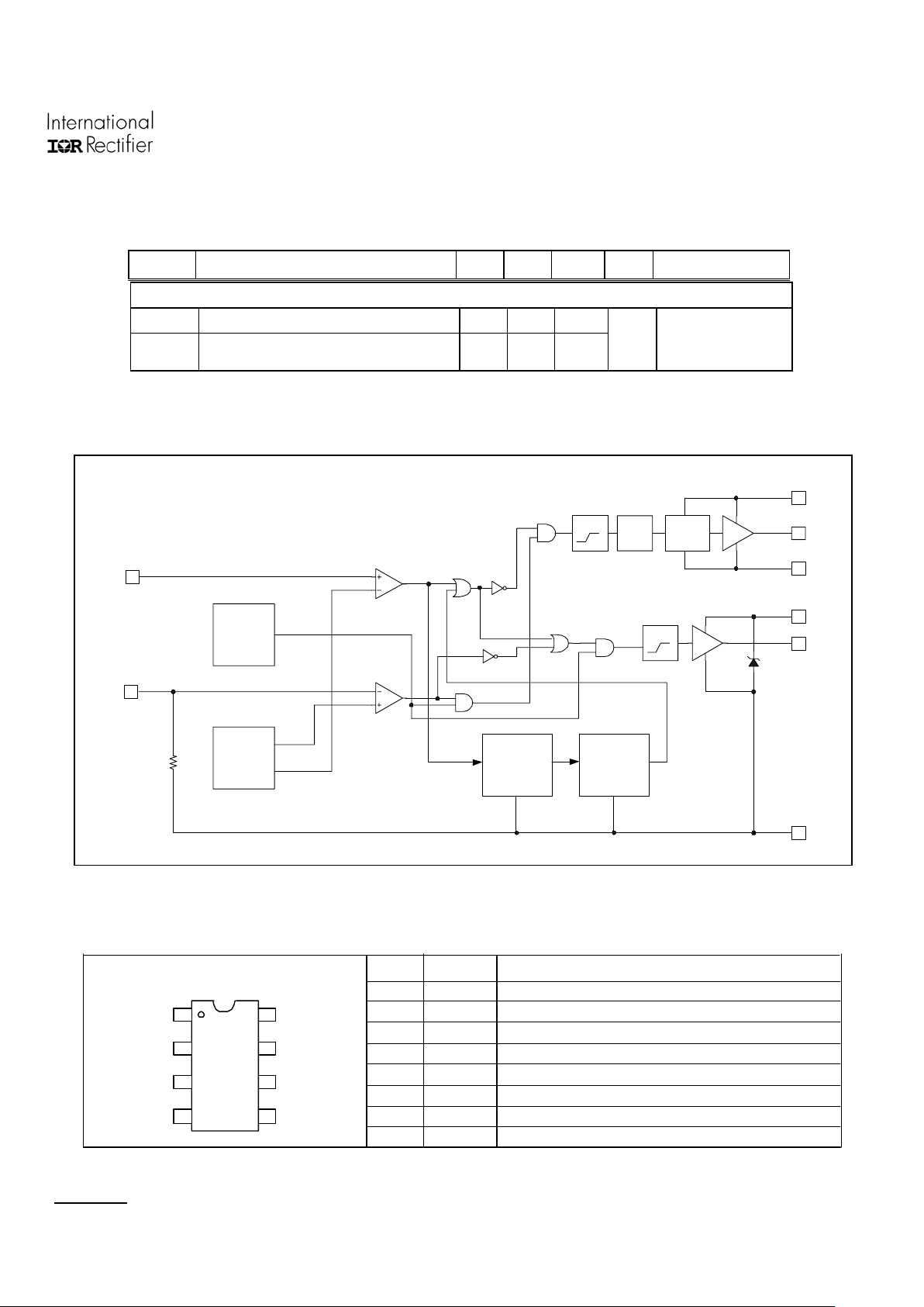
Functional Block Diagram
Values in block diagram are typical values
Lead Assignment
Pin Assignments
Pin # Symbol Description
1
2
3
4
IRS254(0,1)
VCC
COM
ENN
LO
VS
HO
VB
8
7
6
5
IFB
1
3
7
6
5
4
2
IFB
VCC
HO
VS
LO
Current feedback
High-side floating return
High-side gate driver output
8
COM
VB
High-side gate driver floating supply
IC power & signal ground
Supply voltage
ENN Disable outputs (LO=High,HO=Low)
Low
-side gate driver output
Watchdog timer
tWD Watchdog timer period --- 20 ---
P
WWD
LO pulse width --- 1.0 ---
µs
I
FB
=1 V
LEVEL
SHIFT
PULSE
FILTER&
LATCH
7
8
6
VS
HO
VB
1
5
2
COM
LO
VCC
15.6 V
4
ENN
2 V
3
IFB
DELAY
DELAY
UVLO
UVN
0. 5 V
Watchdog
Timer
20 µS
1 µS Pulse
Generator
BANDGAP
REFERENCE
100 K
 Loading...