

IRF IRS21844STRPBF, IRS21844, IRS2184STRPBF, IRS2184 Datasheet
Data Sheet No. PD60252
IRS2184/IRS21844(S)PbF
HALF-BRIDGE DRIVER
Features
Floating channel designed for bootstrap operation
•
Fully operational to +600 V
•
Tolerant to negative transient voltage, dV/dt immune
•
Gate drive supply range from 10 V to 20 V
•
Undervoltage lockout for both channels
•
3.3 V and 5 V input logic compatible
•
Matched propagation delay for both channels
•
Logic and power ground +/- 5 V offset
•
Lower di/dt gate driver for better noise immunity
•
Output source/sink current capability 1.4 A/1.8 A
•
RoHS compliant
•
Description
The IRS2184/IRS21844 are high voltage, high speed power MOSFET and
IGBT drivers with dependent high-side
and low-side referenced output channels. Proprietary HVIC and latch
immune CMOS technologies enable
ruggedized monolithic construction.
The logic input is compatible with standard CMOS or LSTTL output, down to 3.3
V logic. The output drivers feature a
high pulse current buffer stage designed for minimum driver cross-conduction. The floating channel can be
used to drive an N-channel power MOSFET or IGBT in the high-side configuration which operates up to 600 V.
Feature Comparison
Part
2181 COM
21814
2183 Internal 400 COM
21834
2184 Internal 400 COM
21844
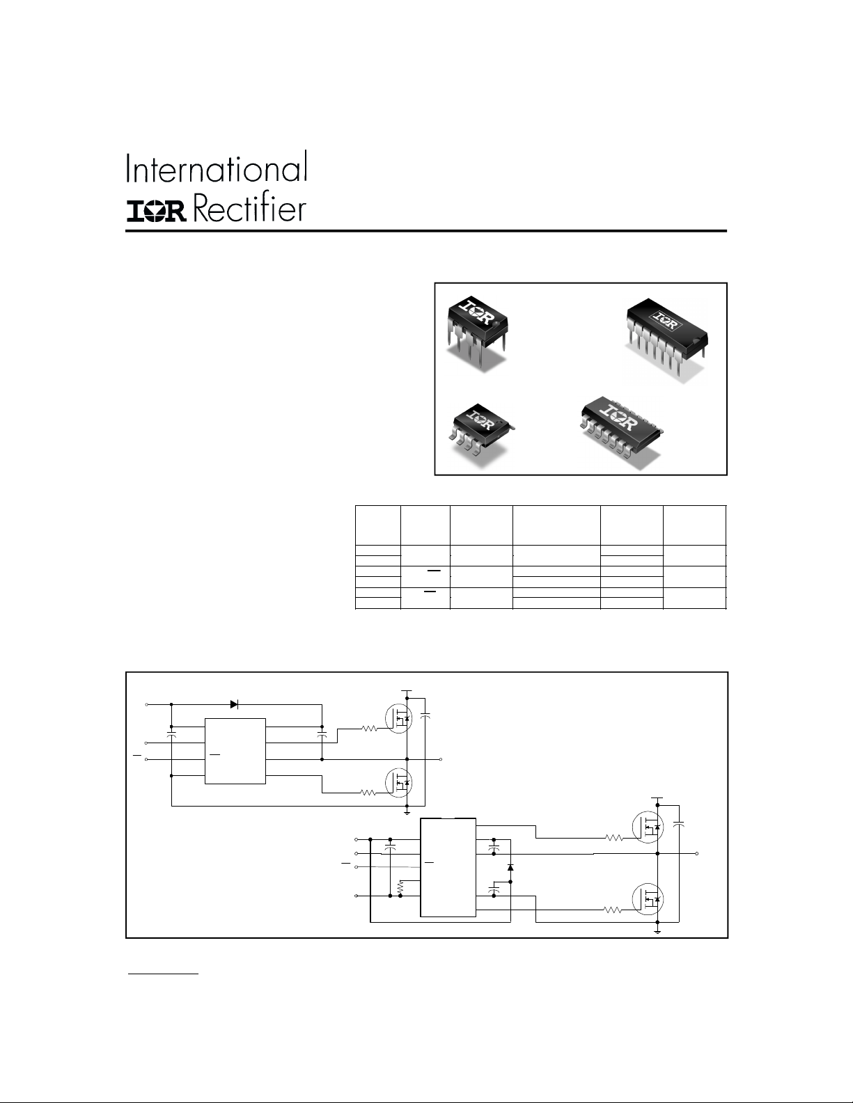
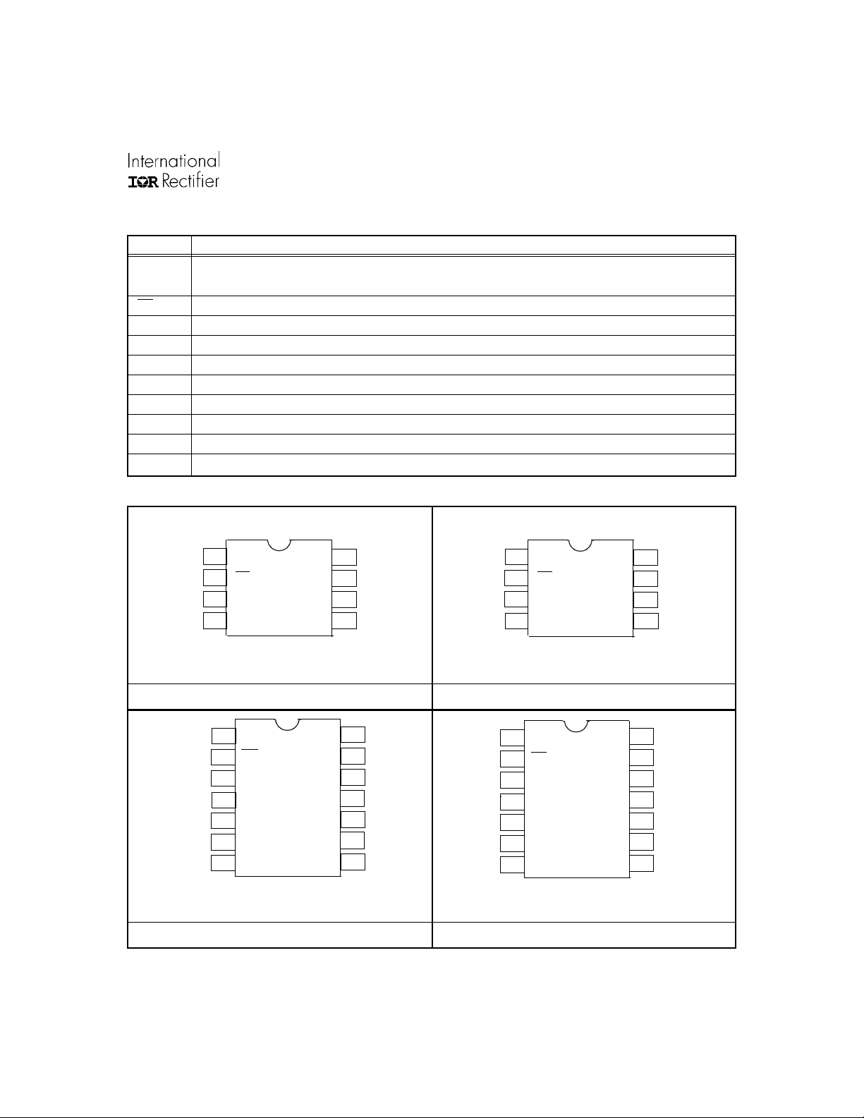
Packages
8-Lead PDIP
IRS2184
8-Lead SOIC
IRS2184S
Input
logic
HIN/LIN no none
HIN/LIN yes
IN/SD yes
Crossconduction
prevention
logic
Deadtime
(ns)
Program 400-5000 VSS/COM
Program 400-5000 VSS/COM
14-Lead PDIP
IRS21844
Ground Pins
VSS/COM
14-Lead SOIC
IRS21844S
ton/t
off
(ns)
180/220
180/220
680/270
Typical Connection
V
CC
V
IN
SD
(Refer to Lead Assignments for correct
configuration).These diagrams show
electrical connections only. Please refer
to our Application Notes and DesignTips
for proper circuit board layout.
IN
SD
V
CC
HO
B
V
S
LOCOM
IRS2184
V
CC
IN
SD
V
SS
up to 600 V
R
DT
TO
LOAD
up to 600 V
HO
V
V
CC
B
V
IN
SD
DT
V
S
COM
SS
LO
IRS21844
TO
LOAD
www.irf.com 1
IRS2184/IRS21844(S)PbF
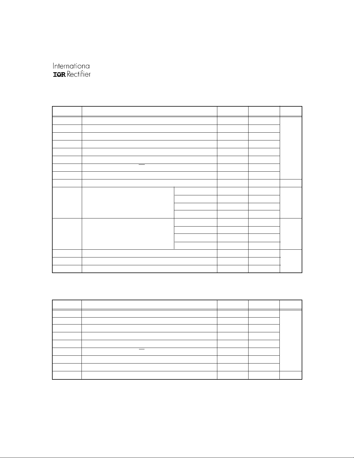
Absolute Maximum Ratings
Absolute maximum ratings indicate sustained limits beyond which damage to the device may occur. All voltage parameters
are absolute voltages referenced to COM. The thermal resistance and power dissipation ratings are measured under board
mounted and still air conditions.
Symbol Definition Min. Max. Units
V
B
V
S
V
HO
V
CC
V
LO
DT Programmable deadtime pin voltage (IRS21844 only) VSS - 0.3 V
V
IN
V
SS
dVS/dt Allowable offset supply voltage transient — 50 V/ns
P
D
RthJ
T
J
T
S
T
L
Note 1: All supplies are fully tested at 25 V and an internal 20 V clamp exists for each supply.
Recommended Operating Conditions
The input/output logic timing diagram is shown in Fig. 1. For proper operation the device should be used within the
recommended conditions. The VS and VSS offset rating are tested with all supplies biased at a 15 V differential.
Symbol Definition Min. Max. Units
VB High-side floating supply absolute voltage VS + 10 VS + 20
V
S
V
HO
V
CC
V
LO
V
IN
DT Programmable deadtime pin voltage (IRS21844 only) V
V
SS
T
A
Note 2: Logic operational for VS of -5 V to +600 V. Logic state held for VS of -5 V to -VBS. (Please refer to the Design Tip
DT97-3 for more details).
High-side floating absolute voltage -0.3 620 (Note 1)
High-side floating supply offset voltage VB - 20 VB + 0.3
High-side floating output voltage VS - 0.3 VB + 0.3
Low-side and logic fixed supply voltage -0.3 20 (Note 1)
Low-side output voltage -0.3 VCC + 0.3
Logic input voltage (IN & SD) VSS - 0.3 V
Logic ground (IRS21844 only) V
- 20 V
CC
(8-lead PDIP) — 1.0
Package power dissipation @ TA ≤ +25 °C
(14-lead PDIP) — 1.6
(8-lead SOIC) — 0.625
(14-lead SOIC) — 1.0
(8-lead PDIP) — 125
Thermal resistance, junction to ambient
A
(8-lead SOIC) — 200
(14-lead PDIP) — 75
(14-lead SOIC) — 120
Junction temperature — 150
Storage temperature -50 150
Lead temperature (soldering, 10 seconds) — 300
High-side floating supply offset voltage Note 2 600
High-side floating output voltage V
S VB
Low-side and logic fixed supply voltage 10 20
Low-side output voltage 0 V
Logic input voltage (IN & SD) V
SS
SS VCC
Logic ground (IRS21844 only) -5 5
Ambient temperature -40 125
CC
CC
CC
V
+ 0.3
+ 0.3
+ 0.3
CC
CC
V
W
°C/W
°C
V
°C
www.irf.com 2
IRS2184/IRS21844(S)PbF
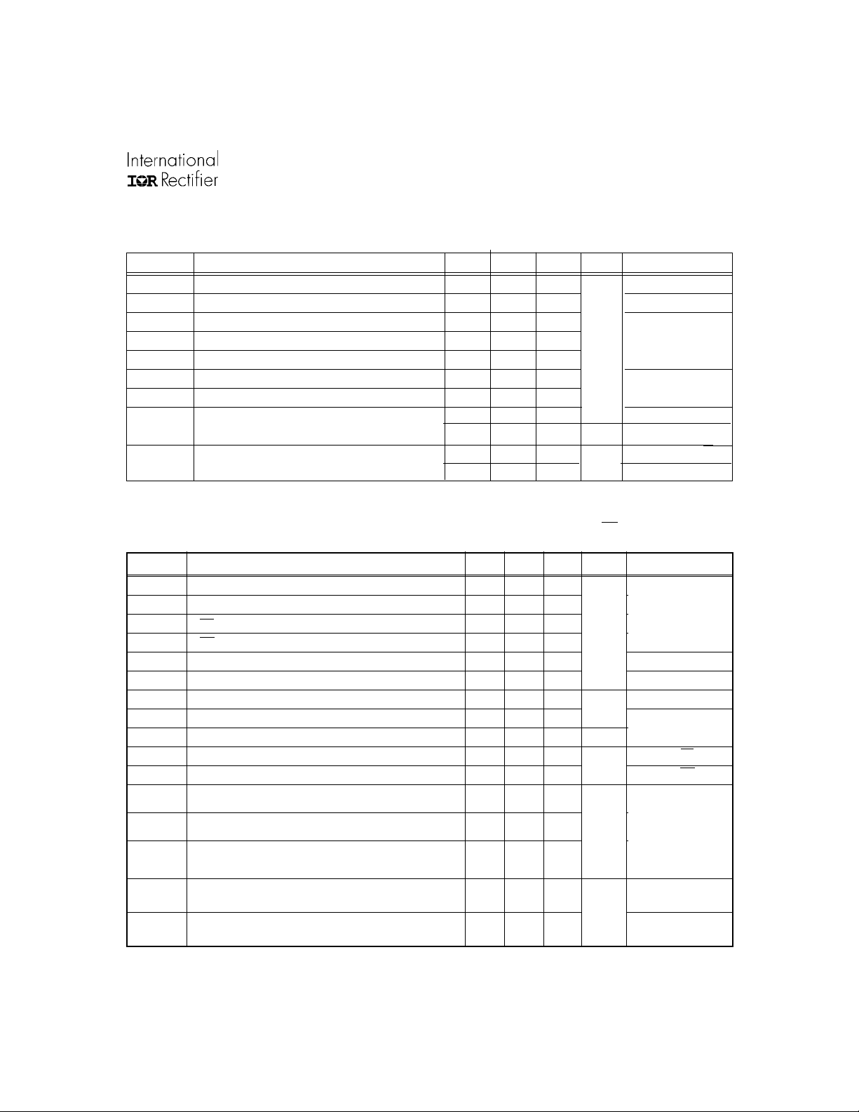
Dynamic Electrical Characteristics
V
(VCC, VBS) = 15 V, VSS = COM, CL = 1000 pF, TA = 25° C, DT = VSS unless otherwise specified.
BIAS
Symbol Definition Min. Typ. Max. Units Test Conditions
t
on
t
off
t
sd Shut-down propagation delay
MTon Delay matching, HS & LS turn-on — 0 90
MToff Delay matching, HS & LS turn-off — 0 4 0
t
t
DT
MDT Deadtime matching = DT
Static Electrical Characteristics
V
BIAS
parameters are referenced to V
Ron parameters are referenced to COM and are applicable to the respective output leads: HO and LO.
Symbol Definition Min. T yp. Max. Units T est Conditions
V
V
V
SD,TH+ SD input positive going threshold 2.5
V
SD,TH- SD input negative going threshold
V
OH
V
OL
I
LK
I
QBS
I
QCC
I
IN+
I
IN-
V
CCUV+
V
BSUV+
V
CCUV-
V
BSUV-
V
CCUVH
V
BSUVH
I
O+
I
O-
Turn-on propagation delay — 680 900 VS = 0 V
Turn-off propagation delay — 270 400 VS = 0 V or 600 V
— 180 270
ns
Turn-on rise time — 40 60
r
Turn-off fall time — 20 35
f
Deadtime: LO turn-off to HO turn-on(DT
HO turn-off to LO turn-on (DT
- DT
LO - HO
HO-LO
LO-HO) &
280 400 520 RDT= 0 Ω
HO-LO)
456µsRDT = 200 kΩ
— 0 50 RDT=0 Ω
ns
— 0 600 RDT = 200 kΩ
(VCC, VBS) = 15 V, VSS = COM, DT= VSS and TA = 25 °C unless otherwise specified. The VIL, V
/COM and are applicable to the respective input leads: IN and SD. The VO, IO, and
SS
Logic “1” input voltage for HO & logic “0” for LO 2.5 — —
IH
Logic “0” input voltage for HO & logic “1” for LO — — 0.8
IL
——
V
µA
High level output voltage, V
Low level output voltage, V
BIAS
O
- V
O
——
— — 1.4 IO = 0 A
— — 0.2 IO = 20 mA
0.8
Offset supply leakage current — — 50 VB = VS = 600 V
Quiescent VBS supply current 20 60 150
Quiescent VCC supply current 0.4 1.0 1.6 mA
Logic “1” input bias current — 25 60 IN = 5 V, SD = 0 V
Logic “0” input bias current — — 5.0 IN = 0 V, SD = 5 V
VCC and VBS supply undervoltage positive going
threshold
VCC and V
supply undervoltage negative going
BS
threshold
8.0 8.9 9.8
7.4 8.2 9.0
µA
V
Hysteresis 0.3 0.7 —
Output high short circuit pulsed current 1.4 1.9 —
A
Output low short circuit pulsed current 1.8 2 .3 —
VS = 0 V
and I
IH,
IN
VCC = 10 V to 20 V
V
= 0 V or 5 V
IN
VO = 0 V,
PW ≤ 10 µs
VO = 15 V,
PW ≤ 10 µs
www.irf.com 3
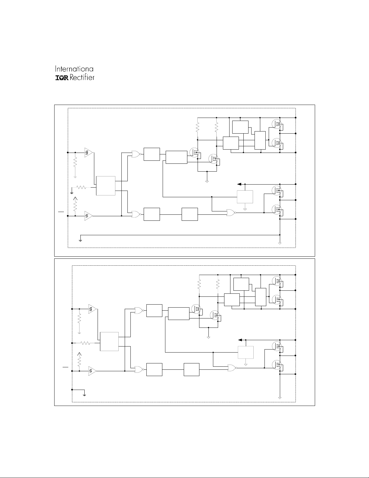
Functional Block Diagrams
2184
IN
VSS/COM
LEVEL
SHIFT
PULSE
GENERATOR
IRS2184/IRS21844(S)PbF
VB
UV
HV
LEVEL
SHIFTER
PULSE
FILTER
DETECT
R
Q
R
S
HO
VS
SD
DT
VCC
LO
COM
+5V
DEADTIME
VSS/COM
LEVEL
SHIFT
DELAY
UV
DETECT
VB
UV
PULSE
FILTER
DETECT
DETECT
R
Q
R
S
HO
VS
VCC
UV
LO
21844
HV
LEVEL
IN
DEADTIME
+5V
VSS/COM
LEVEL
SHIFT
PULSE
GENERATOR
SHIFTER
SD
LEVEL
SHIFT
DELAY
COM
VSS/COM
VSS
www.irf.com 4
IRS2184/IRS21844(S)PbF
Lead Definitions
Symbol Description
IN
SD
DT Programmable deadtime lead, referenced to VSS. (IRS21844 only)
VSS Logic ground (IRS21844 only)
V
B
HO High-side gate drive output
V
S
V
CC
LO Low-side gate drive output
COM Low-side return
Lead Assignments
Logic input for high-side and low-side gate driver outputs (HO and LO), in phase with HO
(referenced to COM for IRS2184 and VSS for IRS21844)
Logic input for shutdown (referenced to
COM for IRS2184 and VSS for IRS21844)
High-side floating supply
High-side floating supply return
Low-side and logic fixed supply
1
IN
2
SD
3
COM
4
LO
V
8
B
HO
7
V
6
S
V
5
CC
1
IN
2
SD
3
COM
4
LO
8-Lead PDIP 8-Lead SOIC
IRS2184PbF IRS2184SPbF
V
HO
V
14
13
B
12
11
S
10
9
8
1
IN
2
SD
3
VSS
4
DT
5
COM
6
LO
7
V
CC
1
IN
2
SD
3
VSS
4
DT
5
COM
6
LO
7
V
CC
14-Lead PDIP 14-Lead SOIC
IRS21844PbF IRS21844SPbF
V
V
HO
V
V
HO
V
CC
B
S
8
B
7
6
S
5
14
13
12
11
10
9
8
www.irf.com 5
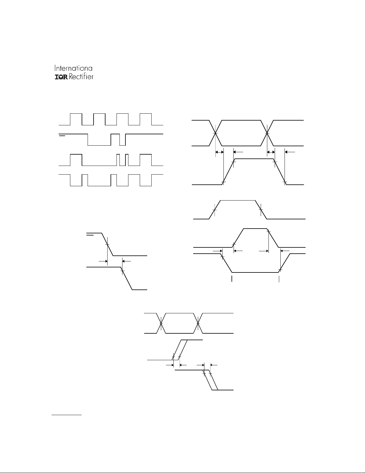
IRS2184/IRS21844(S)PbF
IN
SD
IN(LO)
50%
50%
IN(HO)
HO
LO
LO
HO
t
on
t
r
90% 90%
10% 10%
Figure 1. Input/Output Timing Diagram Figure 2. Switching Time Waveform Definitions
50% 50%
IN
SD
50%
t
sd
HO
90%
LO
Figure 3. Shutdown Waveform Definitions
HO
LO
DT
LO-HO
MDT=
10%
90%
DT
Figure 4. Deadtime Waveform Definitions
LO-HO
t
off
90%
- DT
DT
HO-LO
HO-LO
10%
t
f
IN
(LO)
LO
50%
HO
10%
MT
90%
50%
IN
(HO)
MT
HOLO
Figure 5. Delay Matching Waveform Definitions
www.irf.com 6
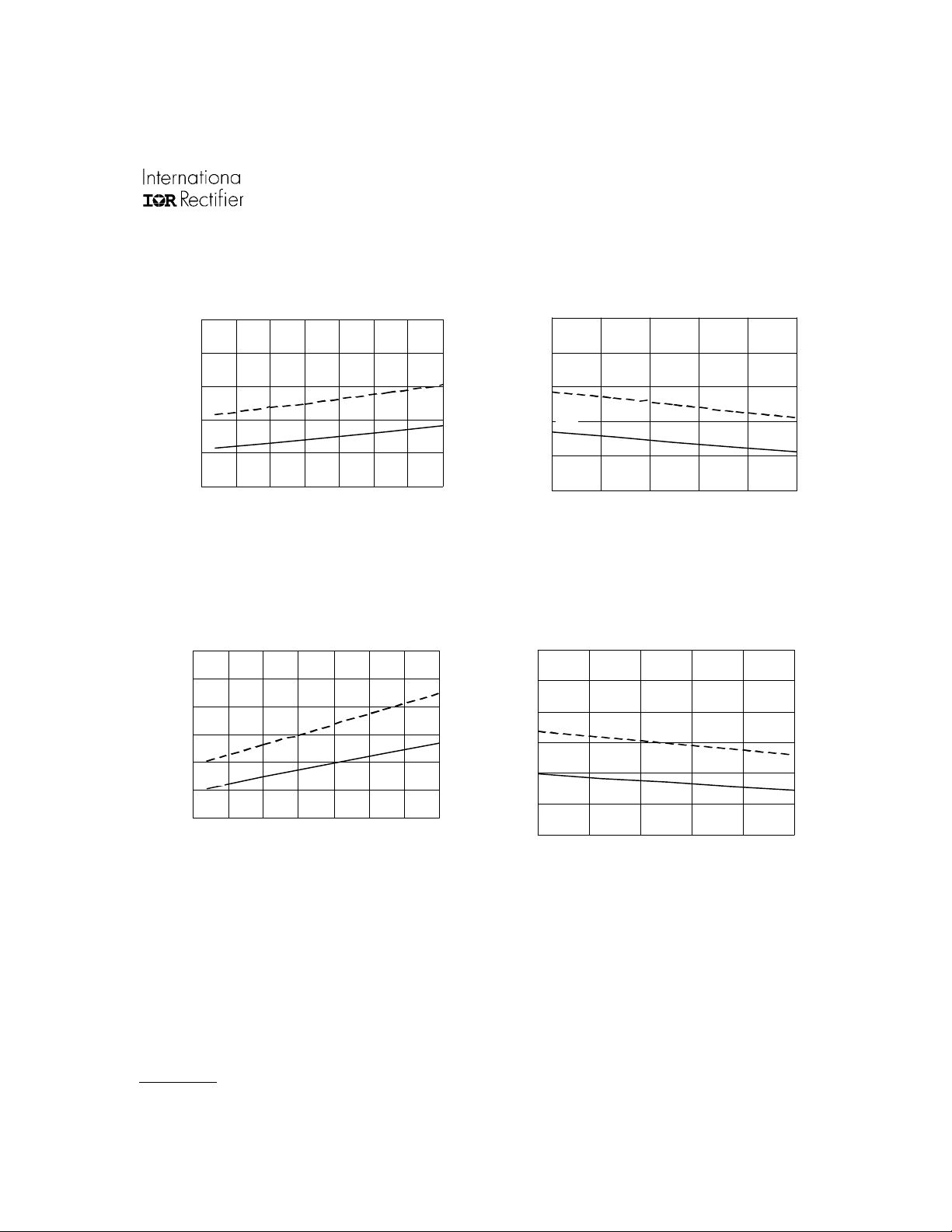
IRS2184/IRS21844(S)PbF
T u r n - o n P r o p a g a t i o n D e l a y ( n s )
T u r n - o n P r o p a g a t i o n D e l a y ( n s )
T u r n - o f f P r o p a g a t i o n D e l a y ( n s )
1400
1200
1000
Max.
800
Typ.
600
400
-50 -25 0 25 50 75 100 125
Temperature (oC)
Figure 6A. Turn-On Propagation Delay
vs. Temperature
700
600
500
400
Max.
300
Typ.
200
100
-50 -25 0 25 50 75 100 125
Temperature (oC)
1400
1200
Max.
1000
Typ.
800
600
400
10 12 14 16 18 20
Supply Voltage (V)
Figure 6B. Turn-On Propagation Delay
vs. Supply Voltage
700
600
500
Max.
400
Typ.
300
200
100
10 12 14 16 18 20
Supply Voltage (V)
Figure 7A. Turn-Off Propagation Delay
vs. Temperature
Figure 7B. Turn-Off Propagation Delay
vs. Supply Voltage
www.irf.com 7
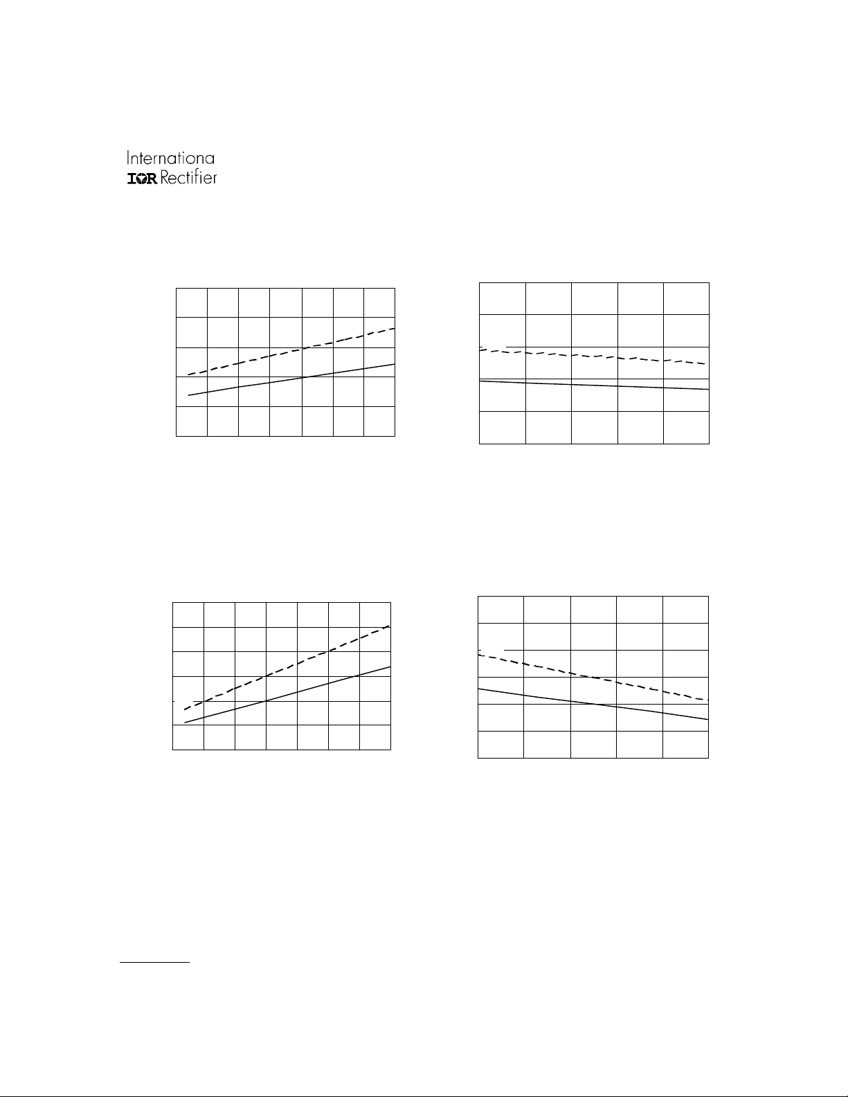
IRS2184/IRS21844(S)PbF
S D P r o p a g a t i o n D e l a y ( n s )
T u r n - O n R i s e T i m e ( n s )
S D P r o p a g a t i o n D e l a y ( n s )
T u r n - O n R i s e T i m e ( n s )
500
400
300
Max.
200
Typ.
100
0
-50 -25 0 25 50 75 100 125
Temperature (oC)
Figure 8A. SD Propagation Delay
vs. Temperature
120
100
80
60
Max
40
Typ.
20
0
-50 -25 0 25 50 75 100 125
Temperature (oC)
500
400
Max.
300
Typ.
200
100
0
10 12 14 16 18 20
Supply Voltage (V)
Figure 8B. SD Propagation Delay
vs. Supply Voltage
120
100
Max.
80
60
Typ.
40
20
0
10 12 14 16 18 20
Supply Voltage (V)
Figure 9A. Turn-On Rise Time vs.
Temperature
Figure 9B. Turn-On Rise Time vs. Supply
Voltage
www.irf.com 8
 Loading...