

D
G
A
D
D
D
S
l Ultra Low On-Resistance
l P-Channel MOSFET
l Surface Mount
l Available in Tape & Reel
l Low Gate Charge
l Lead-Free
PD - 95476A
IRF5806PbF
HEXFET® Power MOSFET
V
DSS
-20V 86mΩ@VGS = -4.5V -4.0A
R
max I
DS(on)
D
147mΩ@VGS = -2.5V -3.0A
Description
These P-channel MOSFETs from International Rectifier
utilize advanced processing techniques to achieve the
extremely low on-resistance per silicon area. This
benefit provides the designer with an extremely efficient
device for use in battery and load management
applications.
The TSOP-6 package with its customized leadframe
produces a HEXFET
®
power MOSFET with R
DS(on)
60% less than a similar size SOT-23. This package is
ideal for applications where printed circuit board space
is at a premium. It's unique thermal design and R
DS(on)
reduction enables a current-handling increase of nearly
300% compared to the SOT-23.
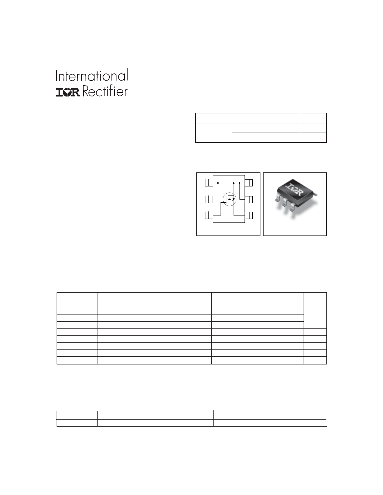
1
2
3
Top View
6
5
4
TSOP-6
Absolute Maximum Ratings
Parameter Max. Units
V
DS
ID @ TA = 25°C Continuous Drain Current, VGS @ -4.5V -4.0
ID @ TA = 70°C Continuous Drain Current, VGS @ -4.5V -3.3 A
I
DM
PD @TA = 25°C Maximum Power Dissipation 2.0 W
PD @TA = 70°C Maximum Power Dissipation 1.3 W
Linear Derating Factor 0.02 W/°C
V
GS
TJ , T
STG
Drain-Source Voltage -20 V
Pulsed Drain Current -16.5
Gate-to-Source Voltage ± 20 V
Junction and Storage Temperature Range -55 to + 150 °C
Thermal Resistance
Parameter Max. Units
R
θJA
www.irf.com 1
Maximum Junction-to-Ambient 62.5 °C/W
8/31/05
IRF5806PbF
S
D
G
Electrical Characteristics @ TJ = 25°C (unless otherwise specified)
Parameter Min. Typ. Max. Units Conditions
V
(BR)DSS
∆V
(BR)DSS
R
DS(on)
V
GS(th)
g
fs
I
DSS
I
GSS
Q
g
Q
gs
Q
gd
t
d(on)
t
r
t
d(off)
t
f
C
iss
C
oss
C
rss
Drain-to-Source Breakdown Voltage -20 ––– ––– V VGS = 0V, ID = -250µA
/∆T
Breakdown Voltage Temp. Coefficient ––– 0.011 ––– V/°C Reference to 25°C, ID = -1mA
J
Static Drain-to-Source On-Resistance
––– 47.1 86 VGS = -4.5V, ID = -4.0A
67.5 147 VGS = -2.5V, ID = -3.0A
mΩ
Gate Threshold Voltage -0.45 ––– -1.2 V VDS = VGS, ID = -250µA
Forward Transconductance 6.4 ––– ––– S VDS = -10V, ID = -4.0A
Drain-to-Source Leakage Current
Gate-to-Source Forward Leakage ––– ––– -100 VGS = -12V
Gate-to-Source Reverse Leakage ––– – –– 100 VGS = 12V
––– ––– -15 VDS = -16V, VGS = 0V
––– ––– -25 VDS = -16V, VGS = 0V, TJ = 70°C
µA
nA
Total Gate Charge ––– 8 .3 11.4 ID = -4.0A
Gate-to-Source Charge ––– 1.2 ––– nC VDS = -16V
Gate-to-Drain ("Miller") Charge ––– 2.6 ––– VGS = -4.5V
Turn-On Delay Time ––– 6.2 9.3 VDD = -10V, VGS = -4.5V
Rise Time ––– 27 41 ID = -1.0A
Turn-Off Delay Time ––– 94 140 RG = 6.0Ω
ns
Fall Time ––– 126 190 RD = 10Ω
Input Capacitance ––– 594 ––– VGS = 0V
Output Capacitance ––– 114 ––– pF VDS = -15V
Reverse Transfer Capacitance ––– 87 ––– ƒ = 1.0MHz
Source-Drain Ratings and Characteristics
Parameter Min. Typ. Max. Units Conditions
I
S
I
SM
V
SD
t
rr
Q
rr
Continuous Source Current MOSFET symbol
(Body Diode) showing the
Pulsed Source Current integral reverse
(Body Diode) p-n junction diode.
-2.0
A
-16.5
Diode Forward Voltage ––– ––– -1.2 V TJ = 25°C, IS = -2.0A, VGS = 0V
Reverse Recovery Time ––– 116 174 ns TJ = 25°C, IF = -2.0A
Reverse Recovery Charge ––– 90 135 nC di/dt = -100A/µs
Notes:
Repetitive rating; pulse width limited by
When mounted on 1 inch square Copper board, t
≤ 10sec.
max. junction temperature.
Pulse width ≤ 300µs; duty cycle ≤ 2%.
2 www.irf.com
IRF5806PbF
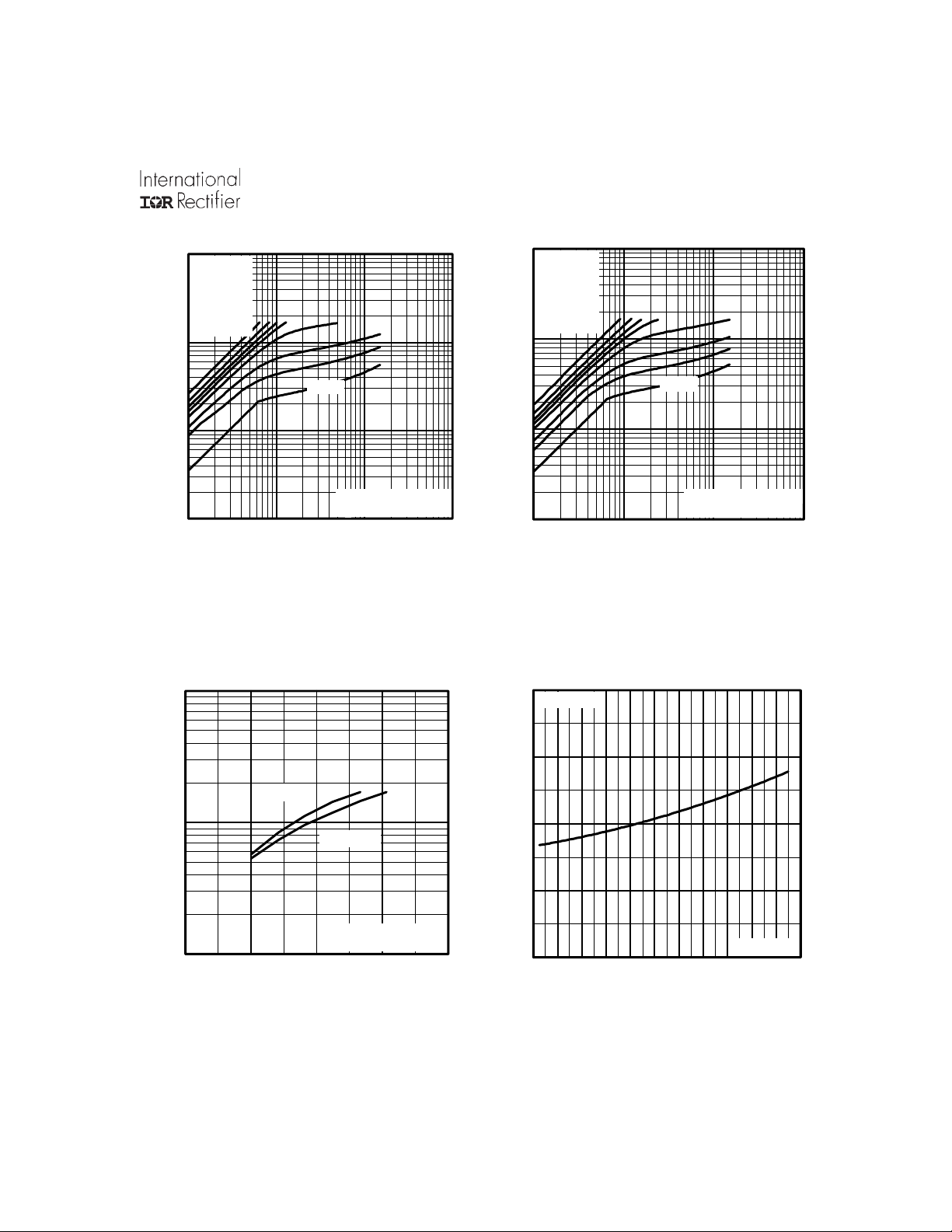
100
10
TOP
BOTTOM
VGS
-7.5V
-5.0V
-4.5V
-3.5V
-3.0V
-2.7V
-2.0V
-1.5V
-1.50V
1
D
-I , Drain-to-Source Current (A)
20µs PULSE WIDTH
°
T = 25 C
0.1
0.1 1 10 100
-V , Drain-to-Source Voltage (V)
DS
J
Fig 1. Typical Output Characteristics
100
100
10
TOP
BOTTOM
VGS
-7.5V
-5.0V
-4.5V
-3.5V
-3.0V
-2.7V
-2.0V
-1.5V
-1.50V
1
D
-I , Drain-to-Source Current (A)
20µs PULSE WIDTH
0.1
0.1 1 10 100
-V , Drain-to-Source Voltage (V)
DS
T = 150 C
°
J
Fig 2. Typical Output Characteristics
2.0
I =
D
-4.0A
1.5
°
T = 25 C
J
10
°
T = 150 C
J
1.0
(Normalized)
D
-I , Drain-to-Source Current (A)
V = -15V
DS
1
1.0 1.5 2.0 2.5 3.0
-V , Gate-to-Source Voltage (V)
GS
20µs PULSE WIDTH
Fig 3. Typical Transfer Characteristics
0.5
DS(on)
R , Drain-to-Source On Resistance
0.0
-60 -40 -20 0 20 40 60 80 100 120 140 160
T , Juncti on Temperature ( C)
J
Fig 4. Normalized On-Resistance
V =
GS
°
-4.5V
Vs. Temperature
www.irf.com 3

IRF5806PbF
1000
800
600
400
V
=
0V,
GS
C
=
C
iss gs gd , ds
C
rss gd
C
oss ds gd
C
iss
+ C
=
C
=
C
+ C
f = 1MHz
C SHORTED
C, Capacitance (pF)
200
0
1 10 100
C
oss
C
rss
-V , Drain-to-Source Voltage (V)
DS
Fig 5. Typical Capacitance Vs.
Drain-to-Source Voltage
100
10
I =
-4.0A
GS
D
8
6
4
2
V =-16V
DS
-V , Gate-to-Source Voltage (V)
0
0 4 8 12 16
Q , Total Gate C harge (nC)
G
Fig 6. Typical Gate Charge Vs.
Gate-to-Source Voltage
100
OPERATION IN THIS AREA LIMITED
BY R
DS(on)
10us
10
°
T = 150 C
J
1
°
T = 25 C
SD
-I , Reverse Drain Current (A)
0.1
0.2 0.6 1.0 1.4
-V ,Source-to-Drain Voltage (V)
SD
J
V = 0 V
GS
Fig 7. Typical Source-Drain Diode
10
100us
1
D
-I , Drain Current (A)I , Drain Current (A)
°
= 25 C
C
T T= 150 C
Single Pulse
0.1
0.1 1 10 100
°
J
-V , Drain-to-Source Voltage (V)
DS
1ms
10ms
Fig 8. Maximum Safe Operating Area
Forward Voltage
4 www.irf.com

IRF5806PbF
+
-
V
DS
9
1
V
t
t
5.0
4.0
3.0
2.0
D
-I , Drain Current (A)
1.0
0.0
25 50 75 100 125 150
T , Case T e mperature ( C)
C
°
Fig 9. Maximum Drain Current Vs.
Case Temperature
100
R
V
DS
V
GS
R
G
V
GS
Pulse Width ≤ 1 µs
Duty Factor ≤ 0.1 %
D
D.U.T.
Fig 10a. Switching Time Test Circuit
d(on)tr
GS
0%
0%
d(off)tf
Fig 10b. Switching Time Waveforms
V
DD
D = 0.50
thJA
0.20
10
0.10
0.05
0.02
0.01
1
SINGLE PU L SE
(THER M AL RESPONSE)
Thermal Response(Z )
Notes:
1. Duty factor D = t / t
2. Peak T = P x Z + T
0.1
0.00001 0.0001 0.001 0.01 0.1 1 10
t , Rectangular Pulse Duration (sec)
1
J DM thJA A
1 2
P
DM
t
1
t
2
Fig 11. Maximum Effective Transient Thermal Impedance, Junction-to-Ambient
www.irf.com 5

IRF5806PbF
V
S
Current Regulator
)
0.20
Ω
(
e
c
n
a
t
s
i
s
0.15
e
R
n
O
e
c
r
u
0.10
o
S
o
t
-
n
i
a
r
0.05
D
,
)
n
o
(
S
D
0.00
R
1.5 2.5 3.5 4.5 5.5 6.5 7.5 8.5
-V
GS,
ID = -4.0A
Gate -to - Source Voltage (V)
)
0.20
Ω
(
e
c
n
a
t
0.16
s
i
s
e
R
n
O
0.12
e
c
r
u
o
S
-
0.08
o
t
-
n
i
a
r
D
,
0.04
)
n
o
(
S
D
0.00
R
0 5 10 15 20
VGS = -2.5V
VGS = -4.5V
-ID , Drain Current ( A )
Fig 12. Typical On-Resistance Vs.
Gate Voltage
Q
G
10 V
Q
GS
G
Q
GD
Charge
Fig 14a. Basic Gate Charge Waveform
Fig 13. Typical On-Resistance Vs.
Drain Current
Same Type as D.U.T.
50KΩ
.2µF
12V
V
GS
.3µF
D.U.T.
-3mA
I
G
Current Sampling Resistors
V
+
I
D
Fig 14b. Gate Charge Test Circuit
D
6 www.irf.com

IRF5806PbF
0.8
0.7
0.6
)
V
(
)
h
t
0.5
(
S
G
V
-
0.4
0.3
0.2
-75 -50 -25 0 25 50 75 100 125 150
TJ , Temperature ( °C )
ID = -250µA
Fig 15. Typical Vgs(th) Vs.
Junction Temperature
100
80
)
60
W
(
r
e
w
o
40
P
20
0
0.0001 0.0010 0.0100 0.1000 1.0000 10.0000
Time (sec)
Fig 16. Typical Power Vs. Time
www.irf.com 7

IRF5806PbF
TSOP-6 Package Outline
TSOP-6 Part Marking Information
W = (1-26) IF PRECEDED BY LAST DIGIT OF CALENDAR YEAR
DATE CODE
Y = YEAR
PART NUMBER
TOP
PART NUMBER CODE REFERENCE:
A = S I3443DV
B = IRF5800
C = IRF 5850
D = IRF5851
E = IRF585 2
F = IRF5801
I = IRF 5805
J = IRF 5806
K = IRF5810
L = IRF 5804
M = IR F5803
N = IRF5802
No te: A line abo ve th e work week
(as s hown here) indicates Lea d-Free.
W = WEE K
LOT
CODE
YEA R
2001Y1
2003
200434
2006
200767
2009
201090
W = (27-52) IF PRECEDED BY A LETTER
2001
2002AB
2004
2005DE
2007
2008GH
2010 K
WORK
WEEK
22002 02
52005
82008
WORK
YYEAR
WEEK
F2006
J2009
W
01
03
04
24
25
26
27
28
30
50
51
A
B
C
D
X
Y
Z
W
A
B
CC2003 29
D
X
Y
8 www.irf.com

TSOP-6 Tape & Reel Information
IRF5806PbF
Data and specifications subject to change without notice.
This product has been designed and qualified for the Consumer market.
Qualifications Standards can be found on IR’s Web site.
IR WORLD HEADQUARTERS: 233 Kansas St., El Segundo, California 90245, USA Tel: (310) 252-7105
TAC Fax: (310) 252-7903
Visit us at www.irf.com for sales contact information.08/05
www.irf.com 9

 Loading...