

IRF IR3820AMTRPbF, IR3820AMPbF Datasheet
01/08/08
1
PD-60330
IR3820AMPbF
HIGHLY INTEGRATED 14A
WIDE-INPUT VOLTAGE, SYNCHRONOUS BUCK REGULATOR
Features
• Wide Input Voltage Range 2.5V to 21V
• Wide Output Voltage Range 0.6V to 12V
• Continuous 14A Load Capability
• 300kHz High Frequency Operation
• Programmable Over-Current Protection
• Programmable PGood Output
• Hiccup Current Limit
• Precision Reference Voltage (0.6V)
• Programmable Soft-Start
• Pre-Bias Start-up
• Thermal Protection
• Thermally Enhanced Package
• Small Size 5mmx6mm QFN
• Pb-Free (RoHS Compliant)
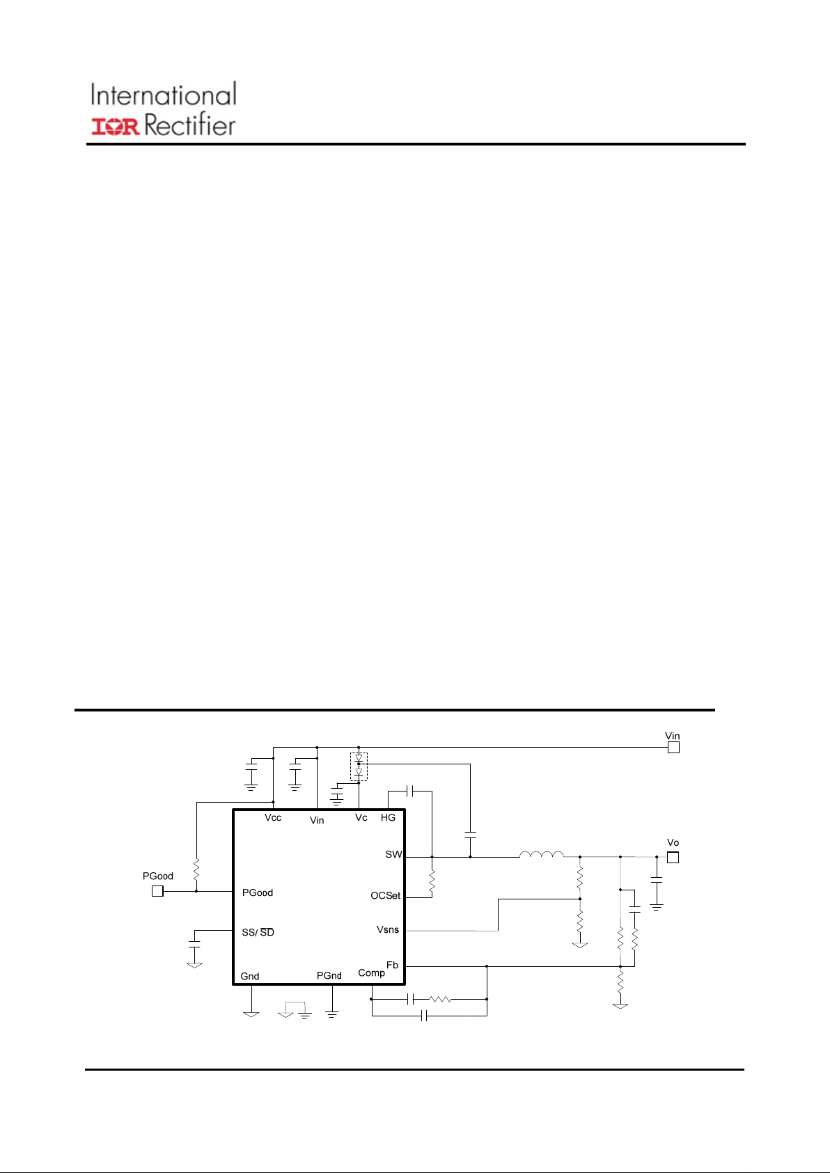
Fig. 1. Typical application diagram
Description
The IR3820A SupIRBuckTMis an easy-to-use,
fully integrated and highly efficient DC/DC
regulator. The onboard switching controller and
MOSFETs make the IR3820A a space-efficient
solution, providing accurate power delivery for
low output voltage applications.
The IR3820A operates from a single 4.5V to 14V
input supply and generates an output voltage
adjustable from 0.6V to 0.75*Vin at loads up to
14A.
A versatile regulator offering programmability of
startup time, power good threshold and current
limit, the IR3820A’s fixed 300kHz switching
frequency allows the use of small external
components.
The IR3820A also features important protection
functions, such as Pre-Bias startup, hiccup
current limit and thermal shutdown to provide the
required system level security in the event of fault
conditions.
Applications
• Distributed Point-of-Loads
• Server and Workstations
• Embedded Systems
• Storage Systems
• DDR Applications
• Graphics Cards
• Game Consoles
• Computing Peripheral Voltage Regulators
SupIRBuck
TM
01/08/08
2
PD-60330
IR3820AMPbF
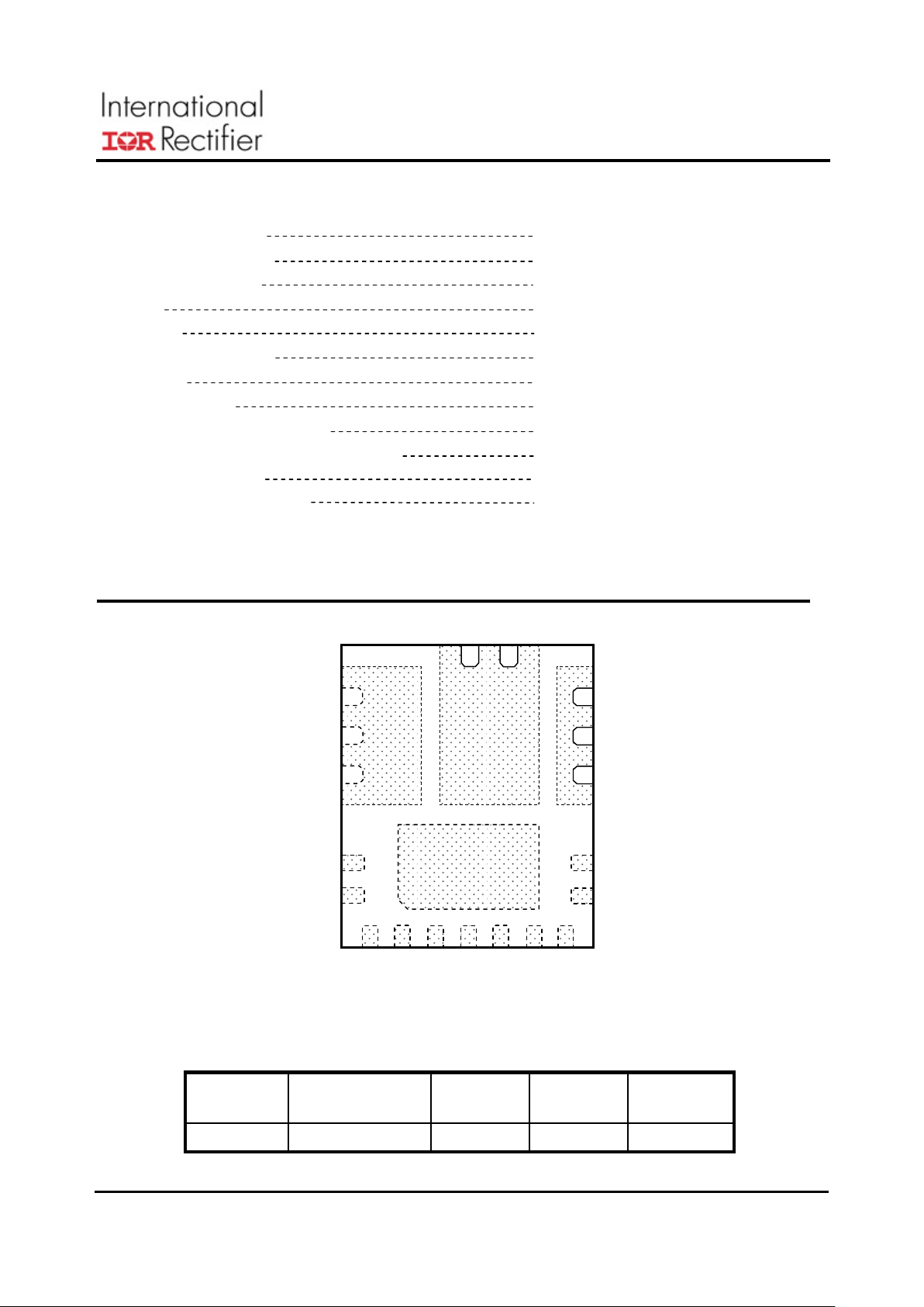
PACKAGE INFORMATION
5mm x 6mm POWER QFN
12
V
IN
11
SW
10
PGnd
15
AGnd
1
23
4
5
6
7
8
9
14
13
Vsns FB COMP AGnd AGnd SS OCSet
PGood
V
CC
V
C
HG
Fig. 2: Package outline (Top view)
W/C2θ
W/C35θ
o
PCBJ
o
JA
=
=
-
ABSOLUTE MAXIMUM RATINGS
(Voltages referenced to GND)
•VINSupply Voltage -0.3V to 24V
• Vcc Supply Voltage -0.3V to 16V
• Vc Supply Voltage -0.3V to 30V
• SW -0.3V to 30V
• PGood -0.3V to 16V
• Fb,COMP,SS,Vsns -0.3V to 3.5V
•OCSet 10mA
• AGnd to PGnd -0.3V to +0.3V
• Storage Temperature Range -65°C To 150°C
• Operating Junction Temperature Range -40°C To 150°C
• ESD Classification JEDEC, JESD22-A114
• Moisture Sensitivity Level JEDEC Level 3 @ 260
o
C
Caution: Stresses beyond those listed under “Absolute Maximum Rating” may cause permanent damage to the
device. These are stress ratings only and functional operation of the device at these or any other conditions beyond
those indicated in the operational sections of the specifications is not implied. Exposure to “Absolute Maximum
Rating” conditions for extended periods may affect device reliability.
4000
PARTS
PER REEL
---------------
PARTS
PER TUBE
15
PIN
COUNT
IR3820AMTRPbF
PACKAGE
DESCRIPTION
M
PKG
DESIG
ORDERING INFORMATION
01/08/08
3
PD-60330
IR3820AMPbF
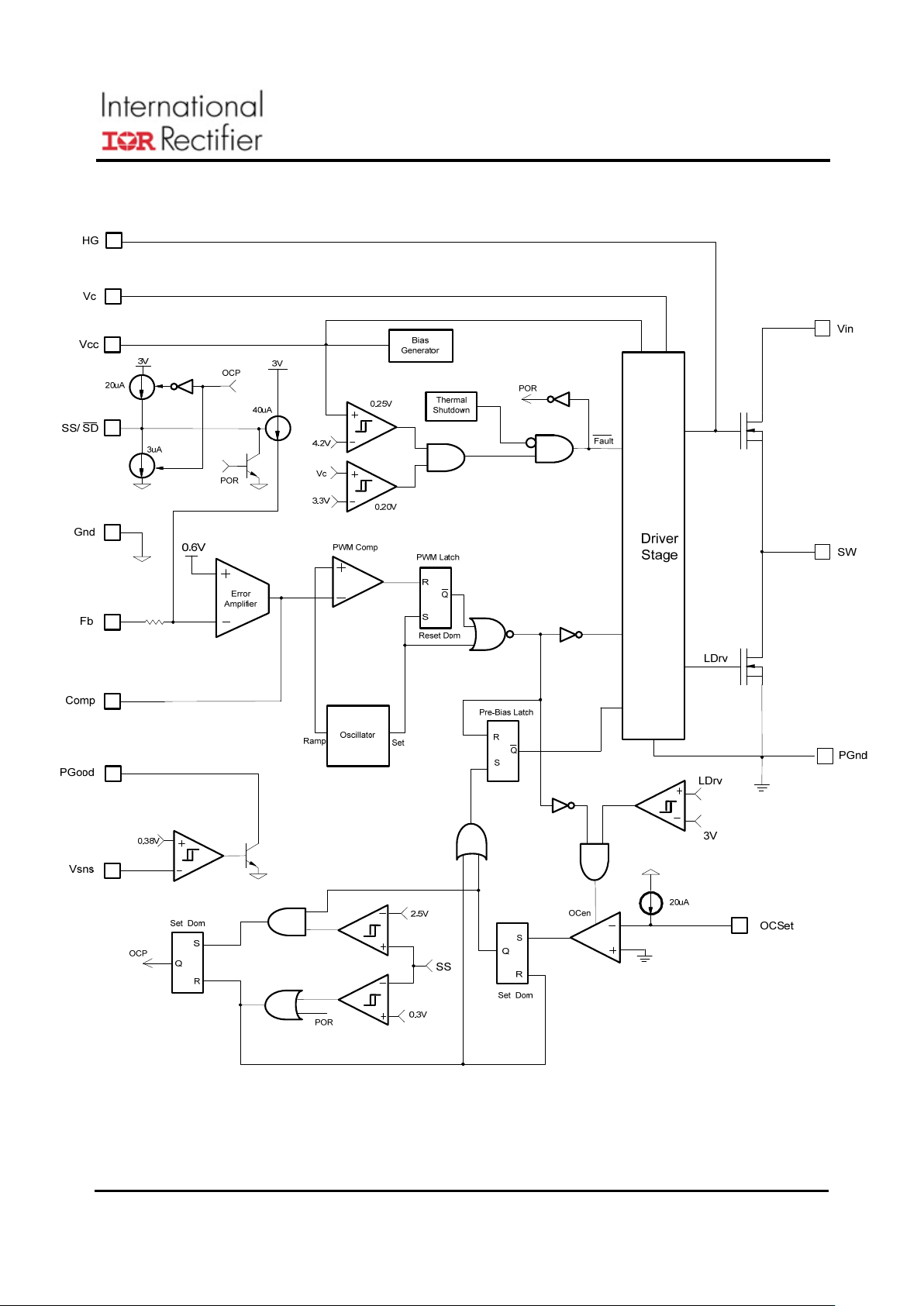
Block Diagram
Fig. 3. Simplified block diagram of the IR3820A.
01/08/08
4
PD-60330
IR3820AMPbF
Pin Description
Pin Name Description
1 Vsns PGood sense pin. Use two external resistors to program the power
good threshold.
2 Fb Inverting input to the error amplifier. This pin is connected directly to the
output of the regulator via resistor divider to set the output voltage and
provide feedback to the error amplifier.
3 Comp Output of error amplifier.
4 AGnd Signal ground for internal reference and control circuitry.
5 AGnd Signal ground for internal reference and control circuitry.
6 SS/SD Soft start / shutdown. This pin provides user programmable soft-start
function. Connect an external capacitor from this pin to signal ground
(AGnd) to set the start up time of the output voltage. The converter can
be shutdown by pulling this pin below 0.3V.
7 OCSet Current limit set point. A resistor from this pin to SW pin will set the
current limit threshold.
8
V
CC
This pin provides biasing voltage for the internal blocks of the IC. It also
powers the low side driver. A minimum of 0.1uF, high frequency
capacitor must be connected from this pin to power ground (PGnd).
9 PGood Power Good status pin. Output is open collector. Connect a pull up
resistor from this pin to Vcc.
10 PGnd Power Ground. This pin serves as a separated ground for the MOSFET
drivers and should be connected to the system’s power ground plane.
11 SW Switch node. This pin is connected to the output inductor
12
V
IN
Input vo ltage connection pi n
13 HG This pin is connected to the high side Mosfet gate. Connect a small
capacitor from this pin to switch node (SW).
14
V
C
This pin powers the high side driver and must be connected to a voltage
higher than input voltage. A minimum of 0.1uF high frequency capacitor
must be connected from this pin to the power ground (PGnd).
15 AGnd Signal ground for internal reference and control circuitry.
Pins 4, 5 and 15 need to be connected together on system board.
01/08/08
5
PD-60330
IR3820AMPbF
Recommended Operating Conditions
Parameter Symbol Test Condition Min TYP MAX Units
Power Loss
Power Loss
P
loss
Vcc=Vin=12V, Vc=24V, Vo=1.8V,
I
o
=14A, L=1.0uH, Note3
3.7 W
MOSFET R
ds(on)
Top Switch
R
ds(on)_Top
I
D
=13A, Tj(MOSFET)=25oC
6.9
8.7
Bottom Switch R
ds(on)_Bot
I
D
=13A, Tj(MOSFET)=25oC
6.9 8.7
mΩ
Reference Voltage
Feedback Voltage VFB 0.6 V
0oC<Tj<105oC -1.35 +1.35 % Accuracy
-40
o
C<Tj<105oC, Note2
-1.5 +1.5 %
Supply Current
VCC Supply Current (Static)
I
CC(Static)
SS=0V, No Switching 10 13
VC Supply Current
(Static)
I
C(Static)
SS=0V, No Switching 4.5 7
VCC Supply Current
(Dynamic)
I
CC(Dynamic)
SS=3V, Vc=24V, Vcc=Vin=12V.
V
o
=1.8V, Io=0A
15 22
VC Supply Current
(Dynamic)
I
C(Dynamic)
SS=3V, Vc=24V, Vcc=Vin=12V.
V
o
=1.8V, Io=0A
15 22
mA
Under Voltage Lockout
VCC-Start-Threshold VCC_UVLO(R) Supply ramping up 4.0 4.4
VCC-Stop-Threshold VCC_UVLO(F) Supply ramping down 3.7 4.1
VCC-Hysteresis Supply ramping up and down 0.15 0.25 0.3
VC-Start-Threshold VC_UVLO(R)
Supply ramping up 3.1 3.5
VC-Stop-Threshold VC_UVLO(F) Supply ramping down 2.85 3.25
VC-Hysteresis Supply ramping up and down 0.15 0.2 0.25
V
Electrical Specifications
Unless otherwise specified, these specification apply over Vin=Vcc=Vc=12V, 0oC<Tj(Ic)<105oC.
Typical values are specified at T
a
= 25oC.
Symbol Definition Min Max Units
Vin Input Voltage 2.5 21
Vcc Supply Voltage 4.5 14
Vc Supply Voltage Vin + 5V 28
Vo Output Voltage 0.6 12
V
I
o
Note1
Output Current 0 14 A
Tj Junction Temperature -40 125
o
C
01/08/08
6
PD-60330
IR3820AMPbF
Note1: Continuous output current determined by input and ou tput voltag e s et ting a nd the the rm al environment.
Note2: Cold temperature performance is guaranteed via correlation using statistical quality control. Not tested in production.
Note3: Guaranteed by Design but not tested in production.
Parameter SYM Test Condition Min TYP MAX Units
Oscillator
Frequency FS
270 300 330 kHz
Ramp Amplitude V
ramp
Note3
1.25 V
Min Pulse Width D
min(ctrl)
Note3
80 ns
Max Duty Cycle D
max
Fb=0V 80 %
Error Amplifier
Input Bias Current I
FB1
SS=3V -0.1 -0.5
Input Bias Current I
FB2
SS=0V 20 35 50
Source/Sink Current I(source/Sink) 50 70 90
μA
Transconductance gm 1000 1300 1600
μmho
Soft Start/SD
Soft Start Current ISS SS=0V 15 20 28
μA
Shutdown Output
Threshold
SD 0.25 V
Power Good
Vsns Low Trip Point Vsns(trip) Vsns Ramping Down 0.35 0.38 0.41 V
Hysteresis PGood(Hys) 15 27.5 40 mV
PGood Output Low
Voltage
PG(voltage) I
PGood
=4mA 0.25 0.5 V
Input Bias Current Isns 0 0.3 1
μA
Over Current Protection
OCSET Current I
OCSET
15 20 26
Hiccup Current I
Hiccup
Note3
3
μA
Hiccup Duty Cycle Hiccup(duty)
I
Hiccup
/ I
SS
,
Note3
15 %
Thermal Shutdown
Thermal Shutdown
Threshold
Note3
140
Thermal Shutdown
Hysteresis
Note3
20
o
C
01/08/08
7
PD-60330
IR3820AMPbF
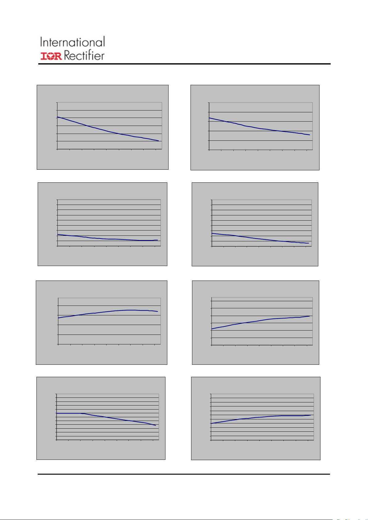
TYPICAL OPERATING CHARACTERISTICS (-40oC - 125oC)
Icc(static)
7.0
8.0
9.0
10.0
11.0
12.0
13.0
-40 -20 0 20 40 60 80 100 120
Temp[oC]
[mA]
Ic(static)
2.0
3.0
4.0
5.0
6.0
7.0
-40 -20 0 20 40 60 80 100 120
Temp[oC]
[mA]
Icc(dynam ic)
13.0
14.0
15.0
16.0
17.0
18.0
19.0
20.0
21.0
22.0
-40-200 20406080100120
Tem p[oC]
[mA]
Ic(dynamic)
13.0
14.0
15.0
16.0
17.0
18.0
19.0
20.0
21.0
22.0
-40 -20 0 20 40 60 80 100 120
Tem p[oC]
[mA]
Vfb
585.0
590.0
595.0
600.0
605.0
-40-200 20406080100120
Temp[oC]
[mV]
ISS
15.0
17.0
19.0
21.0
23.0
25.0
27.0
-40 -20 0 20 40 60 80 100 120
Tem p[oC]
[uA]
Transconductance
1.00
1.05
1.10
1.15
1.20
1.25
1.30
1.35
1.40
1.45
1.50
1.55
1.60
-40-200 20406080100120
Temp[oC]
[mmho]
IOCSET
15.0
16.0
17.0
18.0
19.0
20.0
21.0
22.0
23.0
24.0
25.0
26.0
-40 -20 0 20 40 60 80 100 120
Temp[oC]
[uA]
 Loading...