

IRF IR3651STRPBF, IR3651 Datasheet
IR3651SPbF
10/11/2006
HIGH VOLTAGE SYNCHRONOUS PWM BUCK CONTROLLER
Description
The IR3651 is a high voltage PWM controller
designed for high performance synchronous Buck
DC/DC applications. The IR3651 drives a pair of
external N-MOSFETs using a programmable
switching frequency up to 400kHz allows flexibility
to tune the operation of the IC to meet system
level requirements, and synchronization allows
the simplification of system level filter design. The
output voltage can be precisely regulated using
the internal 1.25V reference voltage for low
voltage applications. Protection such as under
voltage lockout and hiccup current limit are
provided to give required system level security in
the event of fault conditions.
Features
• High Voltage Operating up to 75V
• Programmable Switching Frequency up to 400kHz
• 1A Output Drive Capability
• Precision Reference Voltage (1.25V)
• Programmable Soft-Start
• Programmable Over Current Protection
• Hiccup Current Limit Using MOSFET R
DS(on)
sensing
• External Frequency Synchronization
• 14-pin SOIC Package
Applications
• 48V non-isolated DC to DC Converter
• Embedded Telecom Systems
• Networking and Computing Voltage Regulator
• Distributed Point of Load Power Architectures
• General high voltage DC/DC Converters
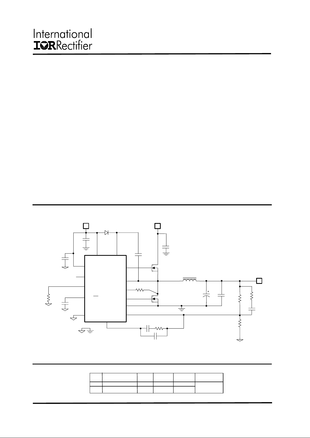
Typical application Circuit
ORDERING INFORMATION
PKG PACKAGE PIN PARTS PARTS T&R
DESIG DESCRIPTION COUNT PER TUBE PER REEL ORIANTAION
S IR3651SPBF 14 55 ------S IR3651STRPBF 14 -------- 2500
Fig A
R
OCset
IR3651S
Vcc
Vb
HDrv
LDrv
Fb
Gnd
Comp
SS/SD
C2
C3
C7
R4
Q1
Q2
L1
Vout
C8
V
aux
=12V
PGnd
SYNC
Vin: 12V-75V
DRVcc
C1
R1
R2
Vs
C4
C6
Rt
R5
C5
C10
C9
R3
OCset
Data Sheet No.PD94720
IR3651SPbF
10/11/2006
ABSOLUTE MAXIMUM RATINGS
(Voltages referenced to GND)
• Vcc, DRVcc Supply Voltage ..................................… -0.3V to 20V
• Vs Supply Voltage …………………………………….. -0.3V to 150V
• Vb Supply Voltage …………………………………….. -0.3V to Vs+20V
• OCset …………….…………………………………….. 10mA
• Storage Temperature Range ..................................... -65°C To 150°C
• Operating Junction Temperature Range ................... -40°C To 150°C
• ESD Classification …………………………………..… JEDEC, JESD22-A114 (1K)
• Moisture Sensitivity Level ……………………………. JEDEC Level 3 @ 260
o
C
CAUTION:
Stresses beyond those listed under “Absolute Maximum Ratings” may cause permanent damage to
the device. These are stress ratings only and functional operation of the device at these or any other conditions
beyond those indicated in the operational sections of the specifications are not implied.
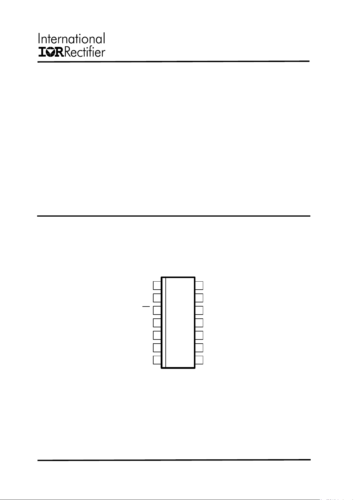
Package Information
14-Pin SOIC NB (S)
2
Θ
JA
= 88.2o C/W
ΘJC= 37o C/W
SYNC
Fb
Vcc
Ldrv
DRVcc
OCset
HDrv
Vs
7
6
5
4
8
9
10
11
3
2
1
12
Rt
13
14
Gnd
PGnd
SS/SD
Comp
Vb
IR3651SPbF
10/11/2006
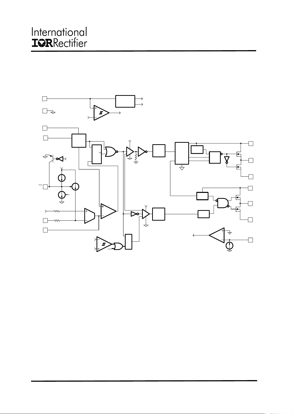
Block Diagram
Fig. 1: Simplified block diagram of the IR3651
3
64uA Max
POR
Oscillator
Error Amp
Ct
Error Com p
Reset Dom
Vcc
Gnd
4.17V
0.25V
Bias
Generator
3V
1.25V
POR
SS/SD
Fb
Comp
25K
25K
3V
R
S
Q
SYNC
Vb
Rt
4
3
1
2
8
11
13
Vcc
DELAY
UV
DETECT
UV Q
S
R
UV
DETECT
HIGH
VOLTAGE
LEVEL
SHIFT
CIRCUIT
LOW
VOLTAGE
LEVEL
SHIFT
LOW
VOLTAGE
LEVEL
SHIFT
HDrv9
Vs
10
DRVcc7
LDrv6
PGND
5
Vcc
1.25V
14
Rt
10uA
OCset
12
OCP
3uA
OCP
20uA
0.3V
SS
Q
R
S
POR
PBias
IR3651SPbF
10/11/2006
Pin Description
Pin Name Description
1 Fb Inverting input to the error amplifier. This pin is connected directly to the
output of the regulator via resistor divider to set the output voltage and
provide feedback to the error amplifier.
2 Comp Output of error amplifier. An external resistor and capacitor network is
typically connected from this pin to ground to provide loop compensation.
3 SS/SD Soft start / shutdown. This pin provides user programmable soft-start
function. Connect an external capacitor from this pin to ground to set the
start up time of the output voltage. The converter can be shutdown by
pulling this pin below 0.3V.
4 SYNC The internal oscillator can be synchronized to an external clock via this
pin.
5 PGnd Power Ground. This pin serves as a separate ground for the MOSFET
driver and should be connected to the system’s power ground plane.
6 LDrv Output driver for low side MOSFET.
7 DRVcc This pin provides biasing for the internal low side driver. A minimum of
0.1uF, high frequency capacitor must be connected from this pin to power
ground.
8 Vb This pin powers the high side driver and must be connected to a voltage
higher than bus voltage. A minimum of 0.1uF, high frequency capacitor
must be connected from this pin to switch node.
9 HDrv Output driver for high side MOSFET
10 Vs Switch node. Connect this pin to the source of the upper MOSFET and
the drain of the lower MOSFET. This pin is return path for the upper gate
driver.
11 Vcc This pin provides power for the internal blocks of the IC. A minimum of
0.1uF, high frequency capacitor must be connected from this pin to
ground.
12 OCSet Current limit set point. A resistor from this pin to drain of low side
MOSFET will set the current limit threshold.
13 Gnd Signal ground for internal reference and control circuitry.
14 Rt Connecting a resistor from this pin to ground sets the oscillator frequency.
4
IR3651SPbF
10/11/2006
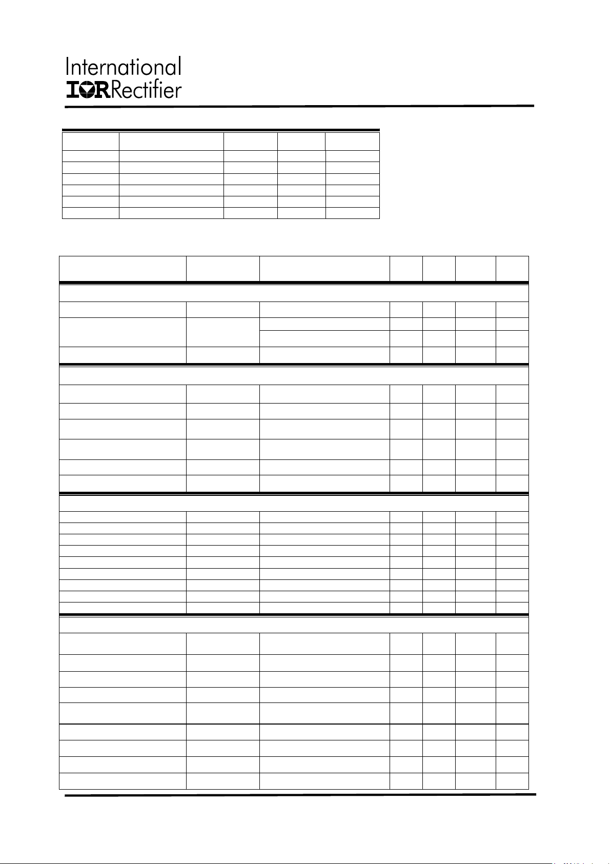
Recommended Operating Conditions
Parameter SYM Test Condition Min TYP MAX Unit
s
Reference Voltage
Feedback Voltage VFB 1.25 V
0oC<Tj<125oC -1.5 +1.5 % Accuracy
-40
o
C<Tj<125oC,
Note1
-3 +1.5 %
Fb Voltage Line Regulation LREG 5V<Vcc<12V 2.0 mV
Supply Current
VCC Supply Current (Stat)
I
CC(Static)
SS=0V, No Switching 6 7 mA
VCC Supply Current (Dyn) I
CC(Dynamic)
Fs=200kHz, C
LOAD
=1.5nF 6 7 mA
DRVcc Supply Current (Stat) I
C(Static)
SS=0V, No Switching 0.3 0.5 mA
DRVcc Supply Current (Dyn) I
C(Dynamic)
Fs=200kHz, C
LOAD
=1.5nF 4 5 mA
Vb Supply Current (Stat) I
b(Static)
SS=0V, No Switching 0.3 0.5 mA
Vb Supply Current (Dyn) I
b(Dynamic)
F
s
=200kHz, C
LOAD
=1.5nF 4.5 5.5 mA
Under Voltage Lockout
VCC-Start-Threshold
VCC_UVLO(R)
Supply ramping up 4.0 4.17 4.35 V
VCC-Stop-Threshold
VCC_UVLO(F)
Supply ramping down 3.75 4.1 V
VCC-Hysteresis
Supply ramping up and down 0.15 0.25 0.3 V
DRVcc-Start-Threshold
DRcc_UVLO(R)
Supply ramping up 8.3 9 9.7 V
DRVcc-Stop-Threshold
DRVcc_UVLO(F)
Supply ramping down 7.5 8.2 8.9 V
DRVCc-Hysteresis
Supply ramping up and down 0.6 0.9 V
Vb-Start-Threshold
Vb_UVLO(R)
Supply ramping up 8.3 9 9.7 V
Vb-Stop-Threshold
Vb_UVLO(F)
Supply ramping down 7.5 8.2 8.9 V
Vb-Hysteresis Supply ramping up and down 0.6 0.9 V
Oscillator
Frequency FS Rt=120K
Rt=51K
170
340
200
400
230
460
kHz
Ramp Amplitude V
ramp
Note2
1.25 V
Min Duty Cycle D
min
Fb=2V 0 %
Min Pulse Width D
min(ctrl)
F
s
=200kHz, Note2
200 ns
Max Duty Cycle D
max
F
s
=200kHz, Fb=1.2V
F
s
=400kHz, Fb=1.2V
80
70
%
Sync Frequency Range Sync(Fs) 20% above free running freq 480 kHz
Sync Pulse Duratin Sync(puls) 200 ns
Sync high Level T hr es hold Sync(H) 2 V
Sync Low Level T hreshold S ync(L) 0.8 V
Electrical Specifications
Unless otherwise specified, these specifications apply over Vcc=5V; DRVcc=Vb=12V, 0oC<Tj< 125oC
5
Symbol Definition Min Max Units
V
bus
Converting Voltage 12 75 V
Vcc Supply Voltage 4.5 13.2 V
DRVcc Supply Voltage 10 16 V
Vb to Vs Supply Voltage 10 16 V
Fs Operating Frequency 100 400 kHz
Tj Junction Temperature -40 125 oC
IR3651SPbF
10/11/2006
Parameter SYM Test Condition Min TYP MAX Units
Error Amplifier
Input Bias Current IFB SS=3V, Fb=1V -0.1 -0.4
µA
Source/Sink Current I(source/Sink) 50 85 120
µA
Transconductance gm 1500 2400 3000
µmho
Soft Start/SD
Soft Start Current ISS SS=0V 15 20 25
µA
Shutdown Output
Threshold
SD 0.25 V
Over Current Protection
OCSET Current I
OCSET
7.5 10 12.5
µA
Hiccup Current I
Hiccup
Note2
3
µA
Hiccup Duty Cycle Hiccup(duty)
I
Hiccup
/ I
SS
, Note2
5 %
Output Drivers
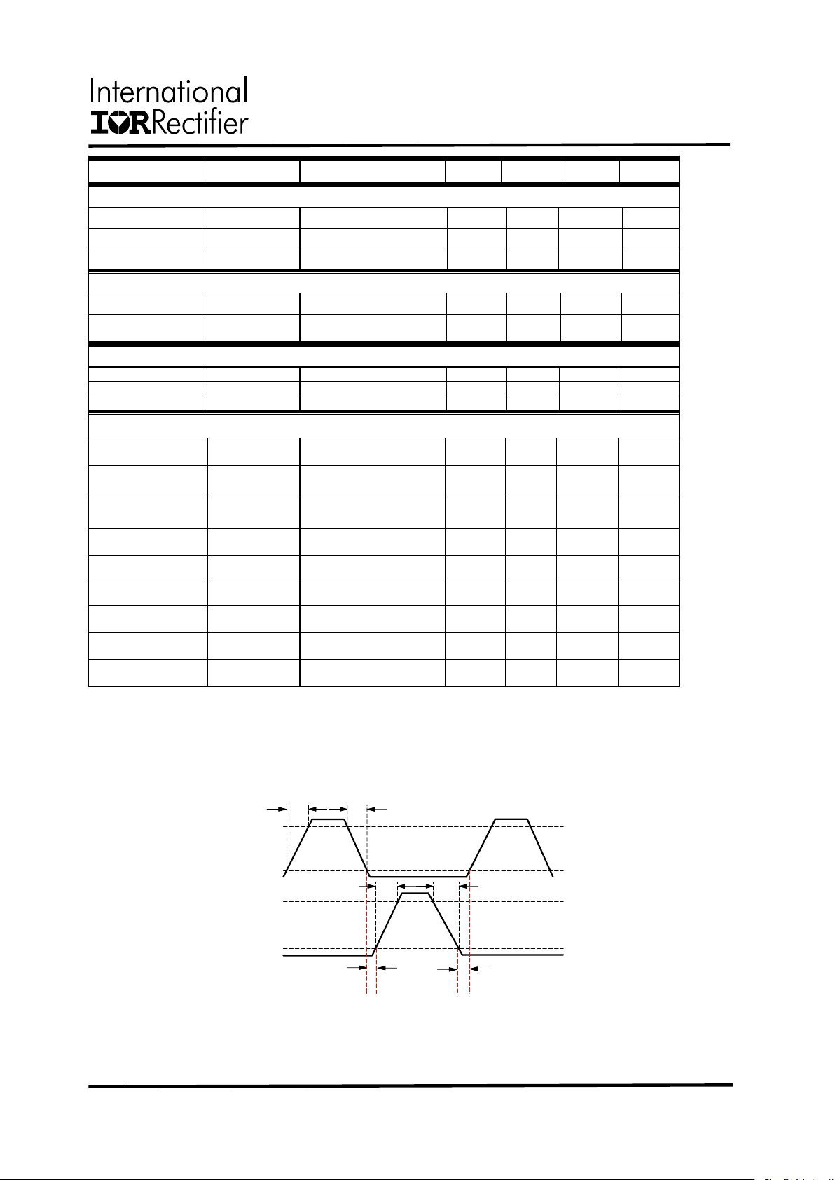
LO, Drive Rise Time Tr(Lo) CL=1.5nF
See Fig 2, Note2
10 20 ns
HI Drive Rise Time Tr(Hi) CL=1.5nF,
See Fig 2, Note2
10 20 ns
LO Drive Fall Time Tf(Lo) CL=1.5nF
See Fig 2,Note2
10 20 ns
HI Drive Fall Time Tf(Hi) CL=1.5nF,
See Fig 2,Note2
10 20 ns
Dead Band Time Tdead See Fig 2 30 45 100 ns
Upper Driver Source
Current
I
upper(source)
HDrv short circuit pulsed
current. PW<10us
1.0 A
Upper Driver Sink
Curret
I
upper(sink)
HDrv short circuit pulsed
current. PW<10us
1.0 A
Lower Driver Source
Current
I
lower(source)
LDrv short circuit pulsed
current. PW<10us
1.0 A
Lower Driver Sink
Current
I
lower(sink)
LDrv short circuit pulsed
current. PW<10us
1.0 A
9V
2V
9V
2V
High Side Driver
(HDrv)
Low Side Driver
(LDrv)
Tr
Tf
Deadband
H_to_L
Deadband
L_to_H
Tr
Tf
Fig. 2: Definition of Rise/Fall time and Deadband Time
6
Note1: Cold temperature performance is guaranteed via correlation using statistical quality control. Not tested in production.
Note2: Guaranteed by Design but not tested in production.
 Loading...