

www.DataSheet4U.com
PD - 94462E
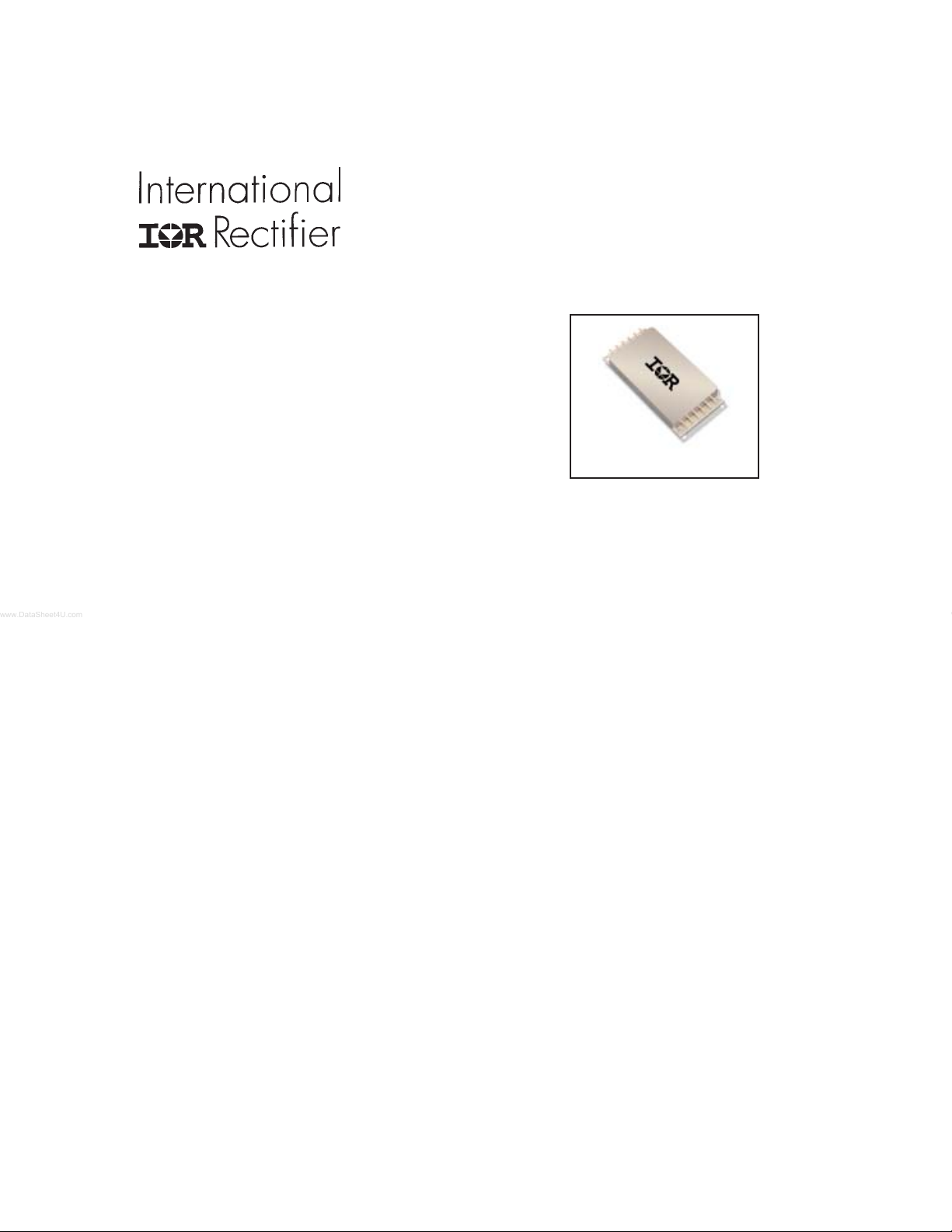
AFL27003R3S
HIGH RELIABILITY
HYBRID DC/DC CONVERTER
Description
The AFL Series of DC/DC converters feature high power
density with no derating over the full military temperature
range. This series is offered as part of a complete family
of converters providing single and dual output voltages
and operating from nominal +28 or +270 volt inputs with
output power ranging from 80 to 120 watts. For
applications requiring higher output power, multiple
converters can be operated in parallel. The internal
current sharing circuits assure equal current distribution
among the paralleled converters. This series
incorporates International Rectifier’s proprietary
magnetic pulse feedback technology providing optimum
dynamic line and load regulation response. This
feedback system samples the output voltage at the pulse
width modulator fixed clock frequency, nominally 550
KHz. Multiple converters can be synchronized to a system
clock in the 500 KHz to 700 KHz range or to the
synchronization output of one converter. Undervoltage
lockout, primary and secondary referenced inhibit, softstart and load fault protection are provided on all models.
These converters are hermetically packaged in two
enclosure variations, utilizing copper core pins to
minimize resistive DC losses. Three lead styles are
available, each fabricated with International Rectifier’s
rugged ceramic lead-to-package seal assuring long
term hermeticity in the most harsh environments.
Manufactured in a facility fully qualified to MIL-PRF38534, these converters are available in four screening
grades to satisfy a wide range of requirements. The CH
grade is fully compliant to the requirements of MIL-PRF38534 for class H. The HB grade is fully processed and
screened to the class H requirement, but does not have
material element evaluated to the class H requirement.
Both grades are tested to meet the complete group “A”
test specification over the full military temperature range
without output power deration. Two grades with more
limited screening are also available for use in less
270V Input, 3.3V Output
AFL
Features
n 160 To 400 Volt Input Range
n 3.3 Volt Output
n High Power Density - 46 W / in
n 66 Watt Output Power
n Parallel Operation with Stress and Current
Sharing
n Low Profile (0.380") Seam Welded Package
n Ceramic Feedthru Copper Core Pins
n High Efficiency - to 74%
n Full Military Temperature Range
n Continuous Short Circuit and Overload
Protection
n Remote Sensing Terminals
n Primary and Secondary Referenced
Inhibit Functions
n Line Rejection > 60 dB - DC to 50KHz
n External Synchronization Port
n Fault Tolerant Design
n Dual Output Versions Available
n Standard Military Drawings Available
demanding applications. Variations in electrical,
mechanical and screening can be accommodated.
Contact IR Santa Clara for special requirements.
3
www.irf.com 1
09/01/04
AFL27003R3S
Specifications
ABSOLUTE MAXI MUM RATI NGS
Input Voltage -0.5V to 500V
Soldering Temperature 300°C for 10 seconds
Case Temperature Operating -55°C to +125°C
Electrical Performance Characteristics -55°C < T
Parameter
INPUT VOLTAGE Note 6 160 270 400 V
OUTPUT VOLTAGE
OUTPUT CURRENT
OUTPUT POWER
MAXIMUM CAPACITIVE LOAD
OUTPUT VOLTAGE
TEMPERATURE COEFFICIENT
OUTPUT VOLTAGE REGULATION
Line
Load
OUTPUT RIPPLE VOLTAGE
INPUT CURRENT
No Load
Inhibit 1
Inhibit 2
INPUT RIPPLE CURRENT
CURRENT LIMIT POINT
Expressed as a
Percentage
of Full Rated Load
LOAD FAULT POWER
DISSIPATION
Overload or Short Circuit
EFFICIENCY
SWITCHING FREQUENCY
ISOLATION
MTBF
For Notes to Specifications, refer to page 3
Storage -65°C to +135°C
< +125°C, 160V< V
CASE
Group A
Subgroups
VIN = 270 Volts, 100% Load
1
2, 3
VIN = 160, 270, 400 Volts, Note 6
Note 6 66 W
4 Note 1 10,000
VIN = 270 Volts, 100% Load - Note 1, 6
1, 2, 3
1, 2, 3
1, 2, 3
2, 3
1, 2, 3
1, 2, 3
1, 2, 3
1, 2, 3
1, 2, 3
1, 2, 3 500 550 600 KHz
No Load, 50% Load, 100% Load
VIN = 160, 270, 400 Volts
VIN = 160, 270, 400 Volts, 100% Load,
BW = 10MHz
VIN = 270 Volts
1
I
= 0
OUT
Pin 4 Shorted to Pin 2
Pin 12 Shorted to Pin 8
VIN = 270 Volts, 100% Load
B.W. = 10MHz
V
= 90% V
OUT
1
2
3
V
= 270 Volts
IN
VIN = 270 Volts, 100% Load
1 Input to Output or Any Pin to Case
(except Pin 3). Test @ 500VDC
MIL-HDBK-217F, AIF @ TC = 40°C
Test Conditions
Note 5
NOM
< 400V unless otherwise specified.
IN
Min Nom Max Unit
3.27
3.23
-0.015 +0.015 %/°C
-10.0
-35.0
115
105
125
72
100
300 KHrs
3.30
20 A
74
3.33
3.37
+10.0
+35.0
30 mVpp
15.0
17.0
3.00
5.00
60 mApp
125
115
140
30
V
V
µfd
mV
mV
mA
mA
mA
mA
%
%
%
W
%
MΩ
2 www.irf.com
Elecrical Performance Characteristics (Continued)
AFL27003R3S
Parameter
ENABLE INPUTS
Sink Current
Converter On
Sink Current
SYNCHRONIZATION INPUT
Pulse Amplitude, Hi
Pulse Amplitude, Lo
Pulse Rise Time
Pulse Duty Cycle
LOAD TRANSIENT RESPONSE
Amplitude
Recovery
Amplitude
Recovery
LINE TRANSIENT RESPONSE
Amplitude
Recovery
TURN-ON CHARACTERISTICS
Overshoot
Delay
LOAD FAULT RECOVERY
LINE REJECTION
Notes to Specifications:
(Inhibit Function)
Converter Off
Frequency Range
Group A
Subgroups
1, 2, 3
1, 2, 3
1, 2, 3
1, 2, 3
1, 2, 3
4, 5, 6
4, 5, 6
4, 5, 6
4, 5, 6
4, 5, 6
4, 5, 6
Logical Low, Pin 4 or Pin 12
Note 1
Logical High, Pin 4 and Pin 12 - Note 9
Note 1
Note 1
Note 1
Note 2, 8
Load Step 50% ⇔ 100%
Load Step 10% ⇔ 50%
Note 1, 2, 3
VIN Step = 160 ⇔ 400 Volts
VIN = 160, 270, 400 Volts. Note 4
Enable 1, 2 on. (Pins 4, 12 high or open)
Same as Turn On Characteristics.
MIL-STD-461, CS101, 30Hz to 50KHz
Note 1
Test Conditions
Min Nom Max Unit
-0.5
2.0
75
500
2.0
-0.5
20
-450
-450
-500
50
60 70 dB
1. Parameters not 100% tested but are guaranteed to the limits specified in the table.
2. Recovery time is measured from the initiation of the transient to where V
has returned to within ±1% of V
OUT
at 50% load.
3. Line transient transition time ≥ 100 µSec.
4. Turn-on delay is measured with an input voltage rise time of between 100 and 500 volts per millisecond.
5. Current limit point is that condition of excess load causing output voltage to drop to 90% of nominal.
6. Parameter verified as part of another test.
7. All electrical tests are performed with the remote sense leads connected to the output leads at the load.
8. Load transient transition time ≥ 10 µSec.
9. Enable inputs internally pulled high. Nominal open circuit voltage ≈ 4.0VDC.
0.8
100
50
100
700
10
0.8
100
80
450
200
450
400
500
500
250
120
V
µ
A
V
µA
KHz
V
V
nSec
%
mV
µSec
mV
µ
Sec
mV
µSec
mV
mSec
OUT
www.irf.com 3

AFL27003R3S
T
2
4
3
5
6
T
-
2
7
9
2
8
T
E
DC INPU
AFL27003R3S Circuit Description
Figure I. AFL Single Output Block Diagram
INPUT
1
FILTER
ENABLE 1
SYNC OUTPU
SYNC INPU
CAS
INPUT RE TURN
PRIMARY
BIAS SUPPLY
CONTROL
Circuit Operation and Application Information
The AFL series of converters employ a forward switched
mode converter topology. (refer to Figure I.) Operation of
the device is initiated when a DC voltage whose magnitude
is within the specified input limits is applied between pins 1
and 2. If pin 4 is enabled (at a logical 1 or open) the primary
bias supply will begin generating a regulated housekeeping
voltage bringing the circuitry on the primary side of the
converter to life. Two power MOSFETs used to chop the
DC input voltage into a high frequency square wave, apply
this chopped voltage to the power transformer. As this
switching is initiated, a voltage is impressed on a second
winding of the power transformer which is then rectified and
applied to the primary bias supply. When this occurs, the
input voltage is shut out and the primary bias voltage
becomes exclusively internally generated.
The switched voltage impressed on the secondary output
transformer winding is rectified and filtered to provide the
converter output voltage. An error amplifier on the
secondary side compares the output voltage to a precision
reference and generates an error signal proportional to the
difference. This error signal is magnetically coupled through
the feedback transformer into the controller section of the
converter varying the pulse width of the square wave signal
driving the MOSFETs, narrowing the width if the output
voltage is too high and widening it if it is too low.
Remote Sensing
Connection of the + and - sense leads at a remotely locatled load permits compensation for resistive voltage drop
between the converter output and the load when they are
physically separated by a significant distance. This
connection allows regulation to the placard voltage at the
point of application.When the remote sensing features is
ERROR
AMP
& REF
CURRENT
SENSE
SHARE
AMPLIFIER
SENSE
AMPLIFIER
OUTPUT
FILTER
+ OUTPUT
10
+ SENSE
11
SHARE
1
ENABLE
SENSE
OUTPUT RETURN
not used, the sense leads should be connected to their
respective output terminals at the converter. Figure III.
illustrates a typical application.
Inhibiting Converter Output
As an alternative to application and removal of the DC
voltage to the input, the user can control the converter
output by providing TTL compatible, positive logic signals
to either of two enable pins (pin 4 or 12). The distinction
between these two signal ports is that enable 1 (pin 4) is
referenced to the input return (pin 2) while enable 2 (pin 12)
is referenced to the output return (pin 8). Thus, the user
has access to an inhibit function on either side of the isolation
barrier. Each port is internally pulled “high” so that when
not used, an open connection on both enable pins permits
normal converter operation. When their use is desired, a
logical “low” on either port will shut the converter down.
Figure II. Enable Input Equivalent Circuit
+5.6V
100K
290K
150K
Disable
2N3904
Pin 4 or
Pin 12
Pin 2 or
Pin 8
1N4148
4 www.irf.com

AFL27003R3S
Internally, these ports differ slightly in their function. In use,
a low on Enable 1 completely shuts down all circuits in the
converter while a low on Enable 2 shuts down the secondary
side while altering the controller duty cycle to near zero.
Externally, the use of either port is transparent to the user
save for minor differences in idle current. (See specification
table).
Synchronization of Multiple Converters
When operating multiple converters, system requirements
often dictate operation of the converters at a common
frequency. To accommodate this requirement, the AFL
series converters provide both a synchronization input and
output.
The sync input port permits synchronization of an AFL
converter to any compatible external frequency source
operating between 500 and 700 KHz. This input signal
should be referenced to the input return and have a 10% to
90% duty cycle. Compatibility requires transition times less
th an100 ns, maximum low level of +0.8 volts and a minimum
Figure III. Preferred Connection for Parallel Operation
Power
Input
Optional
Synchronization
Connection
1
Vin
Rtn
Case
AFL
Enable 1
Sync Out
Sync In
6
1
Vin
Rtn
Case
AFL
Enable 1
Sync Out
Sync In
6
high level of +2.0 volts. The sync output of another converter
which has been designated as the master oscillator provides
a convenient frequency source for this mode of operation.
When external synchronization is not required, the sync in
pin should be left unconnected thereby permitting the
converter to operate at its’ own internally set frequency.
The sync output signal is a continuous pulse train set at
550 ±50 KHz, with a duty cycle of 15 ±5%. This signal is
referenced to the input return and has been tailored to be
compatible with the AFL sync input port. Transition times
are less than 100 ns and the low level output impedance is
less than 50 ohms. This signal is active when the DC input
voltage is within the specified operating range and the
converter is not inhibited. This output has adequate drive
reserve to synchronize at least five additional converters.
A typical synchronization connection option is illustrated in
Figure III.
12
Enable 2
Share
+ Sense
- Sense
Return
+ Vout
7
Share Bus
12
Enable 2
Share
+ Sense
- Sense
Return
+ Vout
7
to Load
1
Vin
Rtn
Case
AFL
Enable 1
Sync Out
Sync In
6
(Other Converters)
Parallel Operation-Current and Stress Sharing
Figure III. illustrates the preferred connection scheme for
operation of a set of AFL converters with outputs operating
in parallel. Use of this connection permits equal sharing of
a load current exceeding the capacity of an individual AFL
among the members of the set. An important feature of the
12
Enable 2
Share
+ Sense
- Sense
Return
+ Vout
7
AFL series operating in the parallel mode is that in addition
to sharing the current, the stress induced by temperature
will also be shared. Thus if one member of a paralleled set
is operating at a higher case temperture, the current it provides to the load will be reduced as compensation for the
temperature induced stress on that device.
www.irf.com 5

AFL27003R3S
⎧
⎫
When operating in the shared mode, it is important that
symmetry of connection be maintained as an assurance of
optimum load sharing performance. Thus, converter outputs
should be connected to the load with equal lengths of wire of
the same gauge and sense leads from each converter should
be connected to a common physical point, preferably at the
load along with the converter output and return leads. All
converters in a paralleled set must have their share pins
connected together. This arrangement is diagrammatically
illustrated in Figure III. showing the outputs and sense pins
connected at a star point which is located close as possible
to the load.
As a consequence of the topology utilized in the current
sharing circuit, the share pin may be used for other functions.
In applications requiring a single converter, the voltage
appearing on the share pin may be used as a “current
monitor”. The share pin open circuit voltage is nominally
+1.00v at no load and increases linearly with increasing
output current to +2.20v at full load. The share pin voltage
is referenced to the output return pin.
Thermal Considerations
Because of the incorporation of many innovative
technological concepts, the AFL series of converters is
capable of providing very high output power from a package
of very small volume. These magnitudes of power density
can only be obtained by combining high circuit efficiency
with effective methods of heat removal from the die junctions.
This requirement has been effectively addressed inside the
device; but when operating at maximum loads, a significant
amount of heat will be generated and this heat must be
conducted away from the case. To maintain the case
temperature at or below the specified maximum of 125°C,
this heat must be transferred by conduction to an
appropriate heat dissipater held in intimate contact with the
converter base-plate.
Because effectiveness of this heat transfer is dependent
on the intimacy of the baseplate/heatsink interface, it is
strongly recommended that a high thermal conductivity heat
transferance medium is inserted between the baseplate
and heatsink. The material most frequently utilized at the
factory during all testing and burn-in processes is sold under
the trade name of Sil-Pad® 4001. This particular pro duct
is an insulator but electrically conductive versions are also
available. Use of these materials assures maximum surface
contact with the heat dissipator thereby compensating
for minor variations of either surface. While other available
types of heat conductive materials and compounds may
provide similar performance, these alternatives are often
less convinient and are frequently messy to use.
A conservative aid to estimating the total heat sink surface
area (A
temperature rise (∆T) above ambient temperature is given
by the following expression:
HEAT SINK
A HEAT SINK ≈
) required to set the maximum case
143..
085
−
⎫
⎬
−
.
⎭
30
⎧
∆T
⎨
⎩
P80
where
Case temperature rise above ambient
∆T
=
Eff
⎫
1
⎬
1
⎭
⎧
Device dissipation in Watts
PP
==−
As an example, it is desired to maintain the case temperature
of an AFL27015S at ≤ +85°C in an area where the ambient
temperature is held at a constant +25°C; then
OUT
⎨
⎩
∆T = 85 - 25 = 60°C
From the Specification Table, the worst case full load
efficiency for this device is 83%; therefore the power
dissipation at full load is given by
1
P =• −
and the required heat sink area is
⎨
⎩
A =
Thus, a total heat sink surface area (including fins, if any) of
71 in2 in this example, would limit case rise to 60°C above
ambient. A flat aluminum plate, 0.25" thick and of
approximate dimension 4" by 9" (36 in2 per side) would
suffice for this application in a still air environment. Note
that to meet the criteria in this example, both sides of the
plate require unrestricted exposure to the ambient air.
⎬
=• =120
1 120 0 205 24 6
83
.
⎭
⎧
60
⎨
⎩
80 24.6
•
()
..W
−143
.
⎫
⎬
0.85
⎭
−=
30 71
.
2
inHEAT SINK
1
Sil-Pad is a registered Trade Mark of Bergquist, Minneapolis, MN
6 www.irf.com

AFL27003R3S
Input Filter
The AFL270XXS series converters incorporate a LC input
filter whose elements dominate the input load impedance
characteristic at turn-on. The input circuit is as shown in
Figure IV.
Figure IV. Input Filter Circuit
8.4µH
Pin 1
0.54µfd
Pin 2
Undervoltage Lockout
A minimum voltage is required at the input of the converter
to initiate operation. This voltage is set to 150 ± 5 volts. To
preclude the possibility of noise or other variations at the
input falsely initiating and halting converter operation, a
hysteresis of approximately 10 volts is incorporated in this
circuit. Thus if the input voltage droops to 140 ± 4 volts, the
converter will shut down and remain inoperative until the
input voltage returns to ≈ 150 volts.
Output Voltage Adjust
In addition to permitting close voltage regulation of remotely
located loads, it is possible to utilize the converter sense
pins to incrementally increase the output voltage over a
limited range. The adjustments made possible by this method
are intended as a means to “trim” the output to a voltage
setting for some particular application, but are not intended
to create an adjustable output converter. These output
voltage setting variations are obtained by connecting an
appropriate resistor value between the +sense and -sense
pins while connecting the -sense pin to the output return pin
as shown in Figure V. below. The range of adjustment and
corresponding range of resistance values can be determined
by use of the following equation.
R = 100
adj
•
⎧
⎨
⎩
V
NOM
- -.025
VV
OUT NOM
⎫
⎬
⎭
Finding a resistor value for a particular output voltage, is
simply a matter of substituting the desired output voltage
and the nominal device voltage into the equation and solving
for the corresponding resistor value.
out
< 500Ω
adj
Adjustment
OUT
R
ADJ
To Load
Figure V. Connection for V
Enable 2
Share
AFL270xxS
+ Sense
- Sense
Return
+ V
Caution: Do not set R
Attempts to adjust the output voltage to a value greater than
120% of nominal should be avoided because of the potential
of exceeding internal component stress ratings and
subsequent operation to failure. Under no circumstance
should the external setting resistor be made less than 500Ω.
By remaining within this specified range of values, completely
safe operation fully within normal component derating limits
is assured.
Examination of the equation relating output voltage and
resistor value reveals a special benefit of the circuit topology
utilized for remote sensing of output voltage in the
AFL270XXS series of converters. It is apparent that as the
resistance increases, the output voltage approaches the
nominal set value of the device. In fact the calculated limiting
value of output voltage as the adjusting resistor becomes
very large is ≈ 25mV above nominal device voltage.
The consequence is that if the +sense connection is
unintentionally broken, an AFL270XXS has a fail-safe output
voltage of Vout + 25mV, where the 25mV is independent of
the nominal output voltage. It can be further demonstrated
that in the event of both the + and - sense connections
being broken, the output will be limited to Vout + 440mV.
This 440 mV is also essentially constant independent of the
nominal output voltage. While operation in this condition is
not damaging to the device, not at all performance
parameters will be met.
Where V
= device nominal output voltage, and
NOM
V
= desired output voltage
OUT
www.irf.com 7

AFL27003R3S
AFL27003R3S Case Outlines
Case X
3.000
2.760
1
6
2.500
2.975 max
0.238 max
12
7
1.260 1.500
0.380
Max
ø 0.128
0.250
1.000
Ref
0.220
0.050
0.200 Typ
Non-cum
Pin
ø 0.040
Case W
Pin Variation of Case Y
0.250
1.000
0.220
2.800
0.525
Case Y Case Z
Pin Variation of Case Y
2.800
0.250
1.000
Ref
0.220
0.525
12
7
0.300
ø 0.140
1.500 1.750
0.375
0.380
Max
2.00
0.250
1.000
Ref
0.220
0.050
0.200 Typ
Non-cum
Pin
ø 0.040
1.150
0.25 typ
1
6
1.750
2.500
2.975 max
0.238 max
Tolerances, unless otherwise specified: .XX = ±0.010
.XXX = ±0.005
BERYLLIA WARNING: These converters are hermetically sealed; however they contain BeO substrates and should not be ground or subjected to any other
operations including exposure to acids, which may produce Beryllium dust or fumes containing Beryllium
0.380
Max
0.36
0.380
Max
0.050
Pin
ø 0.040
0.050
ø 0.040
0.42
Pin
8 www.irf.com

Available Screening Levels and Process Variations for AFL27003R3S Series.
AFL27003R3S
Requirement
Temperature Range -20 to +85°C -55°C to +125°C -55°C to +125°C -55°C to +125°C
Element Evaluation MIL-PRF-38534
Internal Visual 2017
Temperature Cycle 1010 Cond B Cond C Cond C
Constant Acceleration 2001 500g Cond A Cond A
Burn-in 1015 48hrs @ 85°C 48hrs @ 125°C 160hrs @ 125°C 160hrs @ 125°C
Final Electrical (Group A) MIL-PRF-38534
Seal, Fine & Gross 1014 Cond C Cond A, C Cond A, C Cond A, C
External Visual 2009
MIL-STD-883
Method
& Specification
No
Suffix
25°C 25°C -55, +25, +125°C -55, +25, +125°C
ES
Suffix
9
9
HB
Suffix
9
9
CH
Suffix
9
9
* per Commercial Standards
AFL27003R3S Pin Designation
Pin No. Designation
1 Positive Input
2 Input Return
3 Case
4 Enable 1
5 Sync Output
6 Sync Input
7 Positive Output
8 Output Return
9 Return Sense
10 Positive Sense
11 Share
12 Enable 2
Model
Input Voltage
270 = 270V
28 = 28V
Output Voltage
Part Numbering
AFL 270 03R3 S X / CH
Case Style
W, X, Y, Z
03R3 = 3.3V
Outputs
S = Single
D = Dual
Screening
–
, ES
HB, CH
WORLD HEADQUARTERS: 233 Kansas St., El Segundo, California 90245, Tel: (310) 252-7105
IR SANTA CLARA: 2270 Martin Av., Santa Clara, California 95050, Tel: (408) 727-0500
Visit us at www.irf.com for sales contact information.
Data and specifications subject to change without notice. 09/2004
www.irf.com 9
 Loading...