


Bulletin PD-20744 rev. B 02/06
150EBU04
Ultrafast Soft Recovery Diode
Features
• Ultrafast Recovery
• 175°C Operating Junction Temperature
• Screw Mounting Only
• Lead-Free Plating
Benefits
• Reduced RFI and EMI
• Higher Frequency Operation
• Reduced Snubbing
• Reduced Parts Count
Description/ Applications
These diodes are optimized to reduce losses and EMI/ RFI in high frequency power conditioning systems.
The softness of the recovery eliminates the need for a snubber in most applications. These devices are ideally suited
for HF welding, power converters and other applications where switching losses are not significant portion of the total
losses.
t
= 60ns
rr
I
= 150Amp
F(AV)
VR = 400V
Absolute Maximum Ratings
Parameters Max Units
V
R
I
F(AV)
I
FSM
I
FRM
TJ, T
Square Wave, 20kHz
Cathode to Anode Voltage 400 V
Continuous Forward Current, TC = 104°C 150 A
Single Pulse Forward Current, TC = 25°C 1500
Maximum Repetitive Forward Current 300
Operating Junction and Storage Temperatures - 55 to 175 °C
STG
Case Styles
PowIRtab
www.irf.com
1

150EBU04
Bulletin PD-20744 rev. B 02/06
Electrical Characteristics @ T
= 25°C (unless otherwise specified)
J
Parameters Min Typ Max Units Test Conditions
VBR, VrBreakdown Voltage, 400 - - V IR = 200µA
Blocking Voltage
V
F
I
R
C
L
Forward Voltage - 1.07 1.3 V IF = 150A
- 0.9 1.1 V IF = 150A, TJ = 175°C
- 0.96 1.17 V IF = 150A, TJ = 125°C
Reverse Leakage Current - - 50 µA VR = VR Rated
--4mATJ = 150°C, VR = VR Rated
Junction Capacitance - 100 - pF VR = 400V
T
Series Inductance - 3.5 - nH Measured lead to lead 5mm from package body
S
Dynamic Recovery Characteristics @ TJ = 25°C (unless otherwise specified)
Parameters Min Typ Max Units Test Conditions
t
I
RRM
Q
rr
rr
Reverse Recovery Time --60 ns IF = 1.0A, diF/dt = 200A/µs, VR = 30V
I
-93- TJ = 25°C
- 172 - TJ = 125°C
Peak Recovery Current - 11 - A TJ = 25°C
-20- TJ = 125°C
Reverse Recovery Charge - 490 - nC TJ = 25°C
- 1740 - TJ = 125°C
= 150A
F
VR = 200V
diF /dt = 200A/µs
Thermal - Mechanical Characteristics
Parameters Min Typ Max Units
R
thJC
R
thCS
Wt Weight 5.02 g
T Mounting Torque 1.2 2.4 N * m
Mounting Surface, Flat, Smooth and Greased
2
Thermal Resistance, Junction to Case 0.35 K/W
Thermal Resistance, Case to Heatsink 0.2
0.18 (oz)
10 20 lbf.in
www.irf.com
0.001
0.01
0.1
1
10
100
1000
0 100 200 300 400
25˚C
T = 175˚C
J
125˚C
1000
(A)
F
100
10
Instantaneous Forward Current - I
T = 175˚C
J
T = 125˚C
J
T = 25˚C
J
150EBU04
Bulletin PD-20744 rev. B 02/06
(µA)
R
Reverse Current - I
Reverse Voltage - VR (V)
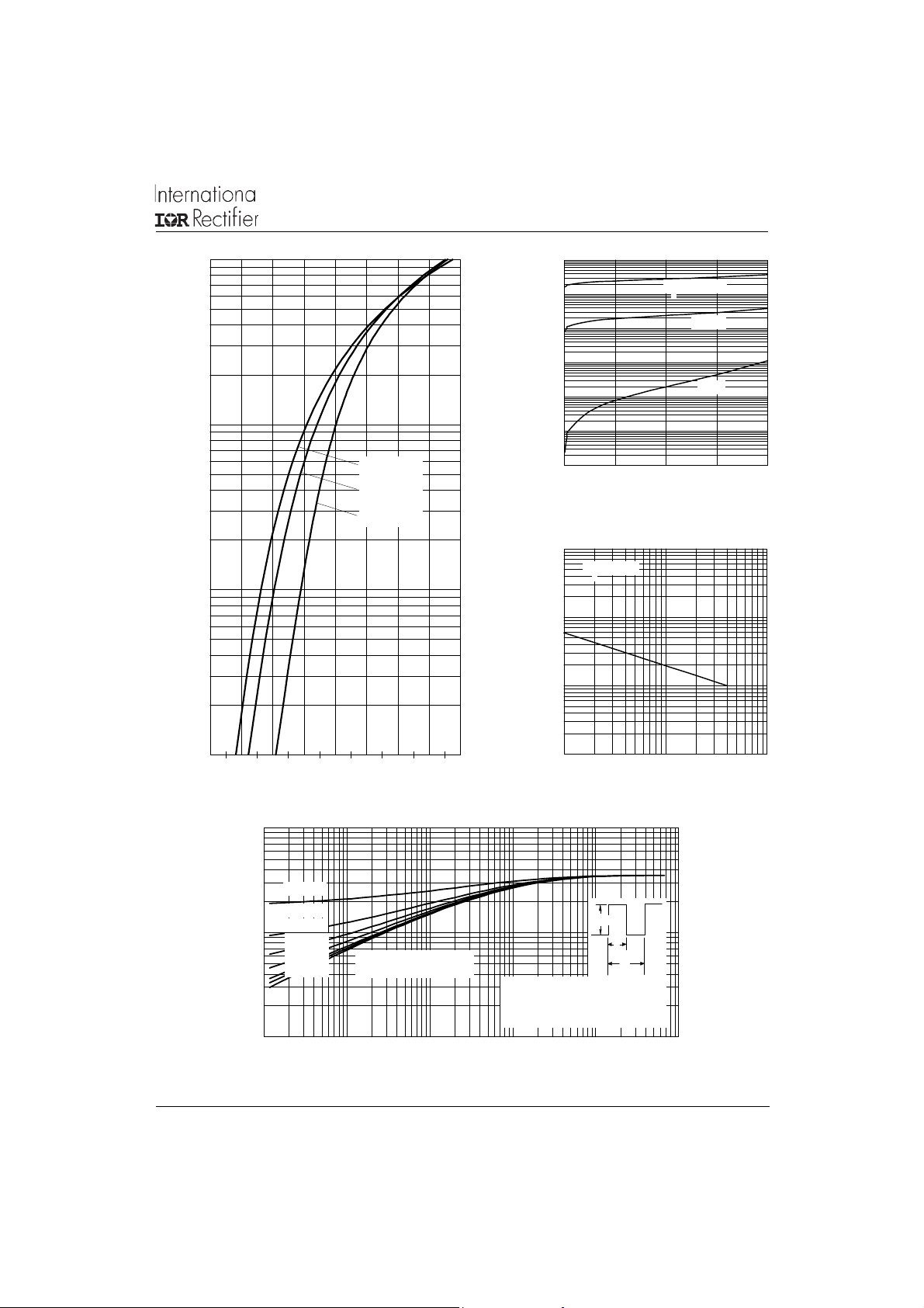
Fig. 2 - Typical Values Of Reverse Current
10000
(pF)
T
1000
Vs. Reverse Voltage
T = 25˚C
J
www.irf.com
1
0.2 0.4 0.6 0.8 1 1.2 1.4 1.6 1.8
Fig. 1 - Typical Forward Voltage Drop Characteristics
Forward Voltage Drop - VFM (V)
1
(°C/W)
thJC
D = 0.50
D = 0.20
D = 0.10
0.1
D = 0.05
D = 0.02
D = 0.01
Thermal Impedance Z
Single Pulse
(Thermal Resistance)
0.01
0.00001 0.0001 0.001 0.01 0.1 1
t1, Rectangular Pulse Duration (Seconds)
Fig. 4 - Max. Thermal Impedance Z
100
Junction Capacitance - C
10
10 100 1000
Reverse Voltage - VR (V)
Fig. 3 - Typical Junction Capacitance
Vs. Reverse Voltage
P
DM
t
1
t
2
Notes:
1. Duty factor D = t1/ t 2
2. Peak Tj = Pdm x ZthJC + Tc
Characteristics
thJC
3

150EBU04
0
500
1000
1500
2000
2500
3000
3500
4000
4500
5000
100 1000
IF = 150A
IF = 75A
Vr = 200V
Tj = 125˚C
Tj = 25˚C
Bulletin PD-20744 rev. B 02/06
180
160
140
DC
120
100
Square wave (D = 0.50)
Rated Vr applied
80
60
Allowable Case Temperature (°C)
see note (3)
40
0 50 100 150 200 250
Average Forward Current - IF
Fig. 5 - Max. Allowable Case Temperature
Vs. Average Forward Current
250
Vr = 200V
Tj = 125˚C
Tj = 25˚C
200
(A)
(AV)
IF = 150A
IF = 75A
300
250
200
150
100
RMS Limit
D = 0.01
D = 0.02
D = 0.05
D = 0.10
DC
50
Average Power Loss ( Watts )
0
0 50 100 150 200 250
Average Forward Current - IF
D = 0.20
D = 0.50
DC
(AV)
Fig. 6 - Forward Power Loss Characteristics
(A)
150
trr ( ns )
100
50
100 1000
di
Fig. 7 - Typical Reverse Recovery time vs. di
(3) Formula used: TC = TJ - (Pd + Pd
Pd = Forward Power Loss = I
Pd
= Inverse Power Loss = VR1 x IR (1 - D); IR @ V
REV
4
/dt (A/µs )
F
REV
x VFM @ (I
F(AV)
) x R
thJC
;
F(AV)
/dt
F
/ D) (see Fig. 6);
= rated V
R1
Qrr ( nC )
di F /dt (A/µs )
Fig. 8 - Typical Stored Charge vs. di
R
/dt
F
www.irf.com

Reverse Recovery Circuit
V = 200V
R
0.01
Ω
L = 70µH
D.U.T.
150EBU04
Bulletin PD-20744 rev. B 02/06
di F /dt
dif/dt
ADJUST
G
Fig. 9- Reverse Recovery Parameter Test Circuit
I
F
t
a
0
1
di F /dt
di /dt
f
1. diF/dt - Rate of change of current through zero
crossing
2. I
- Peak reverse recovery current
RRM
3. t
- Reverse recovery time measured from zero
rr
crossing point of negative going IF to point
where a line passing through 0.75 I
and 0.50 I
current
RRM
extrapolated to zero
Fig. 10 - Reverse Recovery Waveform and Definitions
RRM
3
2
D
IRFP250
S
t
rr
t
b
Q
I
RRM
0.5
di(rec)M/dt
0.75
I
RRM
4. Qrr - Area under curve defined by t
and I
RRM
Q
rr
5. di
/ dt - Peak rate of change of
(rec) M
current during t b portion of t
I
=
4
rr
RRM
t rr x I
2
5
rr
RRM
rr
www.irf.com
5

150EBU04
Bulletin PD-20744 rev. B 02/06
Outline Table
Dimensions in millimeters and (inches)
Ordering Information Table
Device Code
150 E B U 04
52
1
1 - Current Rating (150 = 150A)
2 - Single Diode
3 - PowIRtab (Ultrafast/ Hyperfast only)
4 - Ultrafast Recovery
5 - Voltage Rating (04 = 400V)
Data and specifications subject to change without notice.
This product has been designed and qualified for Industrial Level and Lead-Free.
IR WORLD HEADQUARTERS: 233 Kansas St., El Segundo, California 90245, USA Tel: (310) 252-7105
Visit us at www.irf.com for sales contact information. 02/06
4
3
Qualification Standards can be found on IR's Web site.
TAC Fax: (310) 252-7309
6
www.irf.com

 Loading...