

Features:
Applications:
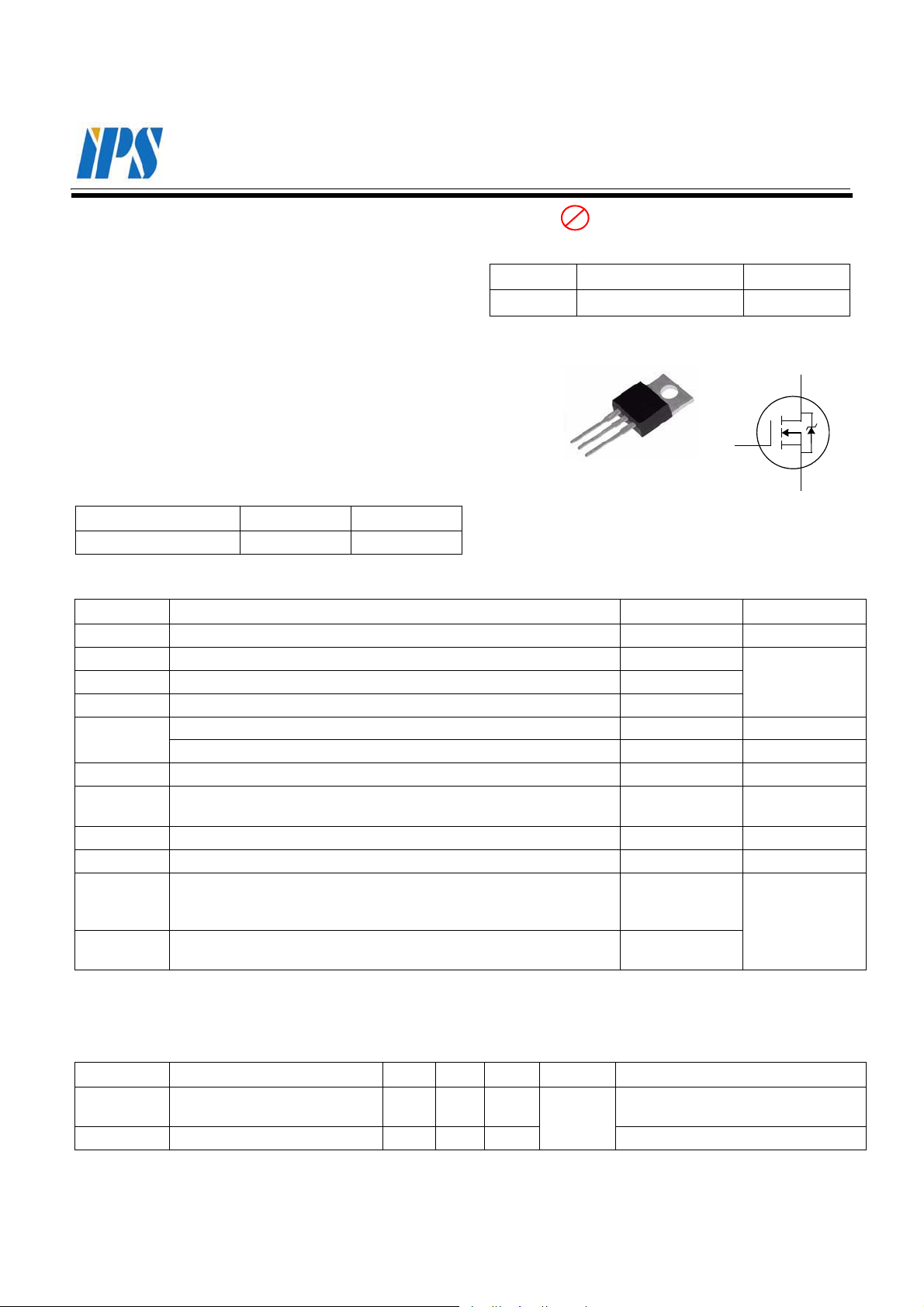
FTP06N03N
Symbol Parameter FTP06N03N Units
Symbol Parameter Min. Typ. Max. Units Test Conditions
Caution:
Pb
N-Channel MOSFET
Lead Free Package and Finish
• Automotive/Telecom
• DC Motor Control
• Class D Amplifier
• Uninterruptible Power Supply (UPS)
V
DSS
R
DS(ON)
(Max.) I
25V 6 m: 65A
• RoHS Compliant
• Low ON Resistance
• Low Gate Charge
• Peak Current vs Pulse Width Curve
G
D
S
Ordering Information
TO-220
Not to Scale
PART NUMBER PACKAGE BRAND
FTP06N03N TO-220 FTP06N03N
o
Absolute Maximum Ratings T
25
C unless otherwise specified
=
C
V
DSS
I
D
@ 100 oC Continuous Drain Current Figure 3
D
I
DM
P
D
V
GS
E
AS
I
AS
dv/dt Peak Diode Recovery dv/dt (NOTE *3) 5.0 V/ns
T
L
T
PKG
T
and T
J
Drain-to-Source Voltage (NOTE *1) 25 V
Continuous Drain Current 65*
Pulsed Drain Current, VGS@ 10V (NOTE *2) Figure 6
Power Dissipation 65 W
o
Derating Factor above 25
Gate-to-Source Voltage ± 20 V
Single Pulse Avalanche Engergy
L=1.0 mH
Pulsed Avalanche Rating Figure 8
Maximum Temperature for Soldering
Leads at 0.063in (1.6mm) from Case for 10 seconds
Package Body for 10 seconds
Operating Junction and Storage
STG
Temperature Range
C0.43W/
-55 to 175
G
205 mJ
300
260
D
D
S
AI
o
C
o
C
*Drain Current limited by Maximum Package Current Rating,50 Amps.
Stresses greater than those listed in the “Absolute Maximum Ratings” Table may cause permanent damage to the device.
Thermal Resistance
R
TJC
R
TJA
Junction-to-Case
Junction-to-Ambient -- -- 62 1 cubic foot chamber, free air.
©2010 InPower Semiconductor Co., Ltd.
-- -- 2.3
Page 1 of 9
o
C/W
Water cooled heatsink, PD adjusted for
a peak junction temperature of +175
FTP06N03N REV. A Jun. 2010
o
C
.

ON Characteristics
Symbol Parameter Min. Typ. Max. Units Test Conditions
OFF Characteristics
Symbol Parameter Min. Typ. Max. Units Test Conditions
Resistive Switching Characteristics
Symbol Parameter Min. Typ. Max. Units Test Conditions
Dynamic Characteristics
Symbol Parameter Min. Typ. Max. Units Test Conditions
Tc=25oC unless otherwise specified
BV
'BV
DSS
DSS
Drain-to-Source Breakdown Voltage 25 -- --
BreakdownVoltage Temperature
/
' T
J
Coefficient, Figure 11.
--
0.08
V
-V/
o
C
VGS=0V, ID=250μA
Reference to 25
I
=250μA
D
o
C,
I
DSS
I
GSS
Drain-to-Source Leakage Current
Gate-to-Source Forward Leakage -- -- 100
Gate-to-Source Reverse Leakage -- -- -100 V
TJ=25
--
-- --
o
unless otherwise specified
C
-- 1
100
μA
nA
=25V, VGS=0V
V
DS
=20V, VGS=0V
V
DS
=150oC
T
c
VGS=+20V
= -20V
GS
V
=10V, ID=30A
GS
(NOTE *4)
=5.0V, ID=16A
V
GS
(NOTE *4)
V
V
=
DS
GS
=15V, ID=35A
V
DS
R
DS(ON)
V
GS(TH)
Static Drain-to-Source On-Resistance
Figure 9 and 10.
Gate Threshold Voltage, Figure 12. 1.0 -- 3.0
gfs Forward Transconductance
-- 5.0 6.0 m:
-- 6.5 9.5 m:
V
--
38
-- S
(NOTE *4)
Essentially independent of operating temperature
C
iss
C
oss
C
rss
Q
g
Q
gs
Q
gd
Input Capacitance -- 1680 --
Output Capacitance -- 260 --
Reverse Transfer Capacitance -- 400 --
Total Gate Charge -- 35 --
Gate-to-Source Charge -- 6.0 --
Gate-to-Drain (“Miller”) Charge -- 14 --
pF
nC
VGS=0V
V
DS
f=1.0MHz
Figure 14
VDD=20V
I
D=15A
V
GS
Figure 15
,
I
=
D
=20V
=10
250PA
V
Essentially independent of operating temperature
t
d(ON)
t
rise
t
d(OFF)
t
fall
©2010 InPower Semiconductor Co., Ltd.
Turn-on Delay Time -- 13 --
Rise Time -- 45 -- ID=15A
Turn-Off Delay Time -- 52 -- VGS=10V
ns
Fall Time -- 55 --
Page 2 of 9
FTP06N03N REV. A Jun. 2010
VDD=20V
=5.1:
R
G

Source-Drain Diode Characteristics
Symbol Parameter Min. Typ. Max. Units Test Conditions
Tc=25oC unless otherwise specified
I
S
I
SM
V
SD
Reverse Recovery Time -- 51 -- ns VGS=0V
t
rr
Q
rr
Continuous Source Current (Body Diode)
Maximum Pulsed Current (Body Diode)
Diode Forward Voltage
Reverse Recovery Charge -- 55 -- nC IF=35A, di/dt=100 A/μs
--
--
-- --
-- 65 A Integral pn-diode
--
260 A
1.5
V
in MOSFET
I
=35A, VGS=0V
S
Notes:
*1. TJ = +25oC to +175oC.
*2. Repetitive rating; pulse width limited by maximum junction temperature.
= 35A di/dt < 100 A/μs, VDD < BV
*3. I
SD
*4. Pulse width <
380μs; duty cycle < 2%.
©2010 InPower Semiconductor Co., Ltd.
, TJ=+175oC.
DSS
Page 3 of 9
FTP06N03N REV. A Jun. 2010

Maximum Continuous Drain Current
vs Case Temperature
Figure 4. Typical Output Characteristics
Typical Drain-to-Source ON Resistance
vs Gate Voltage and Dra
in Current
Maximum Power Dissipation
vs Case Temperature
Figure 1. Maximum Effective Thermal Impedance, Junction-to-Case
Figure 2.
Figure 3.
Figure 5.
Duty Factor
1.000
50%
20%
10%
0.100
5
%
2%
1%
0.010
(Normalized)
, Thermal Impedance
TJC
Z
single pulse
0.001
1E-05 1E-04 1E-03 1E-02 1E-01 1E+00 1E+01
NOTES:
DUTY FACTOR: D= t1/t2
PEAK TJ=PDM x Z
P
DM
tp, Rectangular Pulse Duration (s)
t
TJC
1
t
2
x R
TJC+TC
70
)
W
60
50
40
30
20
, Power Dissipation (
D
P
10
0
25
200
175
150
125
100
75
, Drain Current (A)
D
I
50
25
0
0
50
TC, Case Temperature (
VGS = 15V
VGS = 10V
VGS = 9V
5
V
, Drain-to-Source Voltage (V)
DS
100
75
PULSE DURATION = 10 μS
DUTY FACTOR = 0.5% MAX
T
= 25oC
C
10
125
o
C
15
150
)
VGS = 8V
VGS = 7V
V
G
VGS = 5.5V
VGS = 5V
VGS = 4.5V
80
70
60
50
40
30
, Drain Current (A)
D
I
20
10
0
175
.
=
6
V
S
RDS(ON), Drain-to-Source
20
25
0.040
0.032
0.024
0.016
ON Resistance (:
0.008
0.000
4
Package Limited
75 100
50
T
, Case Temperature (
C
125
150
o
)
C
PULSE DURATION =10 μS
DUTY FACTOR = 0.5% MAX
T
ID = 130A
I
= 65A
D
I
= 30A
D
I
= 15A
D
6789
5
VGS, Gate-to-Source Voltage (V)
10
= 25oC
C
11 12 14 15
13
175
©2010 InPower Semiconductor Co., Ltd.
Page 4 of 9
FTP06N03N REV. A Jun. 2010

Figure 7. Typical Transfer Characteristics
]
Figure 6. Maximum Peak Current Capability
1000
Unclamped Inductive Switching
Capability
Figure 8.
Typical Drain-to-Source
ON
Resistanc
e
vs Junction Temperature
Typical Drain-to-Source ON
Resistance vs Drain Current
Figure 9.
Figure 10.
100
10
, Peak Current (A)
DM
I
VGS = 10V
1
10E-6
TRANSCONDUCTANCE
MAY LIMIT CURRENT IN
THIS REGION
140
PULSE DURATION = 10 μs
DUTY CYCLE = 0.5% MAX
120
TC=25°C
100
80
60
40
20
, Drain-to-Source Current (A)
D
I
0
3.0
+175oC
+25oC
-55oC
4.0
VGS, Gate-to-Source Voltage (V)
FOR TEMPERATURES
ABOVE 25
CURRENT AS FOLLOWS:
100E-6 1E-3 10E-3 100E-3 1E+0 10E+0
o
C DERATE PEAK
,,
---------------------=
7
–
&
tp, Pulse Width (s)
1000
STARTING TJ = 25oC
STARTING TJ = 150oC
)
DSS-VDD
10E-6
)+1
DSS-VDD
100E-6 1E-3 10E-3
tAV, Time in Avalanche (s)
5.0
6.0
7.0
8.0
100
10
, Avalanche Current (A)
AS
I
If R= 0: tAV= (L×IAS)/(1.3BV
If Rz 0: tAV= (L/R) ln[IAS×R)/(1.3BV
R equals total Series resistance of Drain circuit
1
1E-6
VGS = 10V
50
100
150
, Drain-to-Source
R
DS(ON)
0.014
0.012
0.010
0.008
ON Resistance (:)
0.006
PULSE DURATION = 10 μs
DUTY CYCLE = 0.5% MAX
TC=25°C
0
ID, Drain Current (A)
©2010 InPower Semiconductor Co., Ltd.
200
250
, Drain-to-Source
DS(ON)
Resistance (Normalized)
R
Page 5 of 9
2.00
1.75
1.50
1.25
1.00
0.75
0.50
-75 -50 -25 0 25 50
, Junction Temperature (
T
J
PULSE DURATION = 10 μs
DUTY CYCLE = 0.5% MAX
VGS = 10V, ID =30A
100 125
75
150
o
)
C
175
FTP06N03N REV. A Jun. 2010

Typical Breakdown Voltage vs
Junction Temperature
Typical Threshold Voltage vs
Junction Temperature
Figur
e 11.
Figure 12.
Maximum Forward Bias Safe
Operating Area
Figure 13.
Figure 14.
Typical Gate Charge
vs Gate-to-Source Voltage
Typical Body Diode Transfer
Characteristi
cs
Figure 15.
Figure 16.
Typical Capacitance vs
Drain-to-Source Voltage
1.20
1.15
1.10
1.05
, Drain-to-Source
1.00
DSS
BV
0.95
Breakdown Voltage (Normalized)
0.90
-75
-25 0.0 25
-50
TJ, Junction Temperature (oC)
50
75 100
VGS = 0V
ID = 250 μA
125
150
175
1.15
1.10
1.05
1.00
0.95
0.90
0.85
, Threshold Voltage
(Normalized)
0.80
0.75
GS(TH)
V
0.70
0.65
V
=
V
D
S
G
S
I
=
0
2
5
μ
A
D
-75 -50 -25 50
T
250.0
, Junction Temperature (oC)
J
100
75 125
150
175
1000.0
100.0
, Drain Current (A)
D
I
10.0
OPERATION IN THIS AREA
MAY BE LIMITED BY R
1.0
TJ = MAX RATED, TC = 25oC
Single Pulse
0.1
1
V
12
10
8
6
4
DS(ON)
10
, Drain-to-Source Voltage (V)
DS
VDS = 15V
VDS = 30V
VDS = 45V
100000
1
0
s
μ
1
0
μ
0
1
ms
1
0
m
D
C
100 0.1
C, Capacitance (pF)
10000
1000
100
10
VGS = 0V, f = 1MHz
C
= Cgs + C
iss
C
# Cds + C
oss
C
= C
rss
gd
C
iss
C
rss
gd
gd
110
C
oss
100
VDS, Drain Voltage (V)
150
125
100
75
50
175oC
o
C
5
2
2
, Gate-to-Source Voltage (V)
GS
V
0
0 10 20 30 40
, Total Gate Charge (nC)
Q
G
©2010 InPower Semiconductor Co., Ltd.
ID = 30A
, Reverse Drain Current (A)
SD
I
Page 6 of 9
25
0
0.2
0.4
V
SD
0.6
, Source-to-Drain Voltage (V)
0.8
VGS = 0V
1.0
1.2
FTP06N03N REV. A Jun. 2010

Test Circuits and Waveforms
V
DS
V
GS
I
D
D.U.T.
V
DS
I
D
Miller
V
GS
Region
V
DD
V
GS(TH)
1 mA
Figure 17. Gate Charge Test Circuit Figure 18. Gate Charge Waveform
V
R
L
V
DS
V
GS
R
G
D.U.T.
V
DD
DS
V
GS
90%
10%
Q
gs
Q
gd
Q
g
t
d(ON)
Figure 19. Resistive Switching Test Circuit Figure 20. Resistive Switching Waveforms
©2010 InPower Semiconductor Co., Ltd.
Page 7 of 9
t
rise
FTP06N03N REV. A Jun. 2010
t
d(OFF)
t
fall

Test Circuits and Waveforms
di/dt adj.
Current
Pump
Double Pulse
D.U.T.
I
D
Figure 21. Diode Reverse Recovery Test Circuit
I
di/dt = 100A/μA
D
V
DD
Q
rr
L
Figure 22. Diode Reverse Recovery Waveform
t
rr
BV
DSS
Series Switch
(MOSFET)
I
AS
V
DD
V
DD
BV
DSS
D.U.T.
L
Commutating
Diode
V
GS
Figure 23. Unclamped Inductive Switching Test Circuit Figure 24. Unclamped Inductive Switching Waveforms
50:
I
AS
0
V
GS
t
p
E
AS
AS
t
AV
2
LI
2
©2010 InPower Semiconductor Co., Ltd.
Page 8 of 9
FTP06N03N REV. A Jun. 2010

Disclaimers:
InPower Semiconductor Co., Ltd (IPS) reserves the right to make changes without notice in order to improve reliability,
function or design and to discontinue any product or service without notice. Customers should obtain the latest relevant
information before orders and should verify that such information is current and complete. All products are sold subject to
IPS’s terms and conditions supplied at the time of order acknowledgement.
InPower Semiconductor Co., Ltd warrants performance of its hardware products to the specifications at the time of sale,
Testing, reliability and quality control are used to the extent IPS deems necessary to support this warrantee. Except where
agreed upon by contractual agreement, testing of all parameters of each product is not necessarily performed.
InPower Semiconductor Co., Ltd does not assume any liability arising from the use of any product or circuit designs described
herein. Customers are responsible for their products and applications using IPS’s components. To minimize risk, customers
must provide adequate design and operating safeguards.
InPower Semiconductor Co., Ltd does not warrant or convey any license either expressed or implied under its patent rights,
nor the rights of others. Reproduction of information in IPS’s data sheets or data books is permissible only if reproduction is
without modification or alteration. Reproduction of this information with any alteration is an unfair and deceptive business
practice. InPower Semiconductor Co., Ltd is not responsible or liable for such altered documentation.
Resale of IPS’s products with statements different from or beyond the parameters stated by InPower Semiconductor Co., Ltd
for that product or service voids all express or implied warrantees for the associated IPS’s product or service and is unfair and
deceptive business practice. InPower Semiconductor Co., Ltd is not responsible or liable for any such statements.
Life Support Policy:
InPower Semiconductor Co., Ltd’s products are not authorized for use as critical components in life support devices or
systems without the expressed written approval of InPower Semiconductor Co., Ltd.
As used herein:
1. Life support devices or systems are devices or systems which:
a. are intended for surgical implant into the human body,
b. support or sustain life,
c. whose failure to perform when properly used in accordance with instructions
for used provided in the labeling, can be reasonably expected to result in significant
injury to the user.
2. A critical component is any component of a life support device or system whose failure to perform can be reasonably
expected to cause the failure of the life support device or system, or to affect its safety or effectiveness.
©2010 InPower Semiconductor Co., Ltd.
Page 9 of 9
FTP06N03N REV. A Jun. 2010

 Loading...