

IP Mobilenet IPMNDT45TX User Manual

M
440000 –– 551122 M
Hzz
H
Moobbiillee
M
OOwwnneerr’’ss MMaannuuaall
-
Document Control #: DC-94
Version: C-1 (Special Release)
Copyright 2000-2002 IPMobileNet, Inc.
16842 Von Karman Avenue, Suite 200 Irvine, CA 92606
Voice: (949) 417-4590 Fax: (949) 417-4591
Daattaa
D
Date Prepared:
March 1, 2000
Raaddiioo
R

TABLE OF CONTENTS
SECTION 1: THEORY OF OPERATION ................................................................................. 3
General Block Diagram................................................................................................ 3
General Block Diagram Definitions
DT450 Mobile Data Radio Board Circuitry
Microcontroller....................................................................................... 5
Support Circuitry
Input/Output .......................................................................................... 5
Injection Synthesizer ............................................................................. 6
Transmitter ............................................................................................ 6
Receiver 1 Front-End ............................................................................ 6
Receiver 1 IF......................................................................................... 7
Transmit Processing ............................................................................. 7
Baseband Routing................................................................................. 8
Power and Ground ................................................................................ 8
Receiver 2 Front-End ............................................................................ 8
Receiver 2 IF......................................................................................... 9
Modem .................................................................................................. 9
SECTION 2: FACTORY TEST PROCEDURE .......................................................................10
Equipment List ........................................................................................................... 10
Programming and Configuring Mobile Data Radio ................................................. 11
Adjustment / Alignment Procedures ........................................................................ 12
Receiver Injection
Receiver 1
Receiver 2
Transmitter
........................................................................................................ 12
........................................................................................................ 13
....................................................................................................... 14
Power Setting
............................................................................................. 12
................................................................................................... 16
SECTION 3: LABEL AND LABEL PLACEMENT ................................................................ 17
DT450 Mobile Data Radio FCC Label Placement..................................................... 17
DT450 Mobile Data Radio FCC Label........................................................................ 17
APPENDIX A: DT450 MOBILE DATA RADIO CIRCUIT BOARD DIAGRAM....................... 18
..................................................................... 3
......................................................... 5
......................................................................... 5
~\Technical Documentation\System Manuals\FCC-Reports\DT450-FCCRpt.doc Page 2
SECTION 1: THEORY OF OPERATION
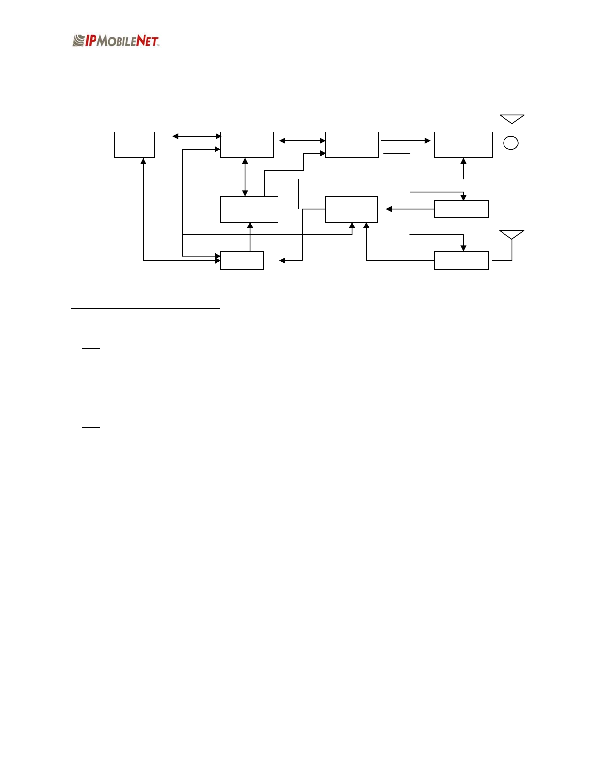
General Block Diagram
DDAATTAA
Input /
Output
Micro-
Controller
Transmit
Processing
General Block Diagram Definitions
For increased data security, the modem supports the U.S. Government developed Digital Encryption
Standard (DES) data encryption and decryption protocols. This capability requires installation of third
party, Internet Protocol (IP) compliant DES encryption and decryption software on the system.
The standard IP circuit board contains ten (10) sections defined below.
These added sections will be discussed in Section 4 of this document.
Input/Output Circuitry associated with the radio’s DB25 data connector providing all the
RS232 data and handshake functions, including the necessary level
changes.
Microcontroller Manages the operation of the radio loading the selected transmit/receive
frequencies into the injection synthesizer, controls the operation of the
modem, and determines which receiver provides a better signal from a
given transmission. Also provides transmit time-out protection in the event
a fault causes the radio to halt in the transmit mode.
Transmit Processing Circuitry that amplifies the analog audio signal from the modem and uses it
to modulate the voltage controlled oscillator (VCO) and 10 MHz reference
oscillator in the injection synthesizer section. Modulating the VCO and
reference oscillator simultaneously results in a higher quality FM signal.
Modem Converts parallel data into an analog audio waveform for transmission and
analog audio from the receiver to serial data. Serial data appears on the
radio’s RS232 port, which connects a Mobile Data Computer (MDC) or a
Voice Interface Unit (VIU).
Injection
Synthesizer
Baseband
Routing
Transmitter
Receiver 1
Receiver 2 Modem
~\Technical Documentation\System Manuals\FCC-Reports\DT450-FCCRpt.doc Page 3

SECTION 1: THEORY OF OPERATION
The modem supports a 115.2 Kbps data transmission rate on the serial
port, SLIP protocol, and up to 19.2 Kbps over-the-air rate. Within a single
chip it provides forward error correction and detection, bit interleaving for
more robust data communications, and third generation collision detection
and correction capabilities.
Injection Synthesizer Provides programmable, ultra stable signals for the radio. One synthesizer
incorporates phase lock loop technology used for both receiving and
transmitting.
High Side Injection In the receive mode, the synthesizer provides a local oscillator signal of 45
MHz above the selected receive channel frequency.
Low Side Injection In the receive mode, the synthesizer provides a local oscillator signal of 45
MHz below the selected receive channel frequency.
Baseband Routing Allows the microcontroller to select one of the two diversity receiver audio
Transmitter Consists of an exciter and power amplifier module. The transmitter covers
Receiver 1/Receiver 2 Required to support the mobile DRS; two (2) discrete receivers are tuned
The receivers are double-conversion superheterodyne with a first
Power Supply Consists of circuitry that derives the various operating voltages for the
In the DT450, due to limitations in synthesizer frequency coverage, high
Low side injection is used for all other receive frequencies. In the
side injection is used for receive frequencies below 456 MHz.
transmit mode, the desired frequency is produced, and it is directly
modulated by the modem. A 10 MHz reference oscillator controls the
synthesizer.
outputs for demodulation by the modem. Switching is done by the
microcontroller comparing the Received Signal Strength Indication (RSSI)
outputs from each receiver. Provision is also made for switching an
external modulation source from the DB25 data connector to the
transmitter input.
the various frequency bands in segments. A different power amplifier
module is required for each segment. The transmitter circuitry includes a
T/R switch, switching the antenna between transmitter and receiver 1
(TX/RX1).
to the same channel and use two (2) antennas.
Intermediate Frequency (IF) of 45 MHz and a second IF frequency of 455
KHz. Each receiver consists of bandpass filters, RF amplifiers, a crystal
filter, a double-balanced mixer, and a one-chip IF system. The injection
synthesizer provides the first local oscillator signal. Outputs from each
receiver include RSSI and analog audio for the baseband routing circuitry
and modem.
radio. A group of fixed and adjustable voltage regulators are used for this
purpose. The transmitter power control circuitry is also found in this
section.
~\Technical Documentation\System Manuals\FCC-Reports\DT450-FCCRpt.doc Page 4

SECTION 1: THEORY OF OPERATION
DT450 Mobile Data Radio Board Circuitry
The DT450 Mobile Data Radio works within a frequency range of 400 to 512 MHz.
The following section provides detail views and key areas on the DT450 Mobile Data Radio circuit board
especially useful during troubleshooting.
Microcontroller
The microcontroller (U43) is a major component of the radio as it manages the operation of the radio
loading the selected transmit/receive frequencies into the injection sythesizer. It also controls the
operation of the modem, and determines which receiver provides a better signal from a given
transmission. It provides transmit time-out protection in the event a fault causes the radio to halt in the
transmit mode. It utilizes a Reduced Instruction Set Computer (RISC) architecture which provides low
power operation and a powerful instruction set. Other features include a watchdog timer, serial UART,
two 8-bit timers, and 2 kB of electrically erasable programmable read only memory (EEPROM) storage.
The EEPROM RAM stores the setup data entered by the technician even if there is a loss of power.
Support circuitry
The support circuitry consists of the following:
A Supervisor Control Chip (U4) providing power-on reset.
The clock controls microcontroller operation and is generated by crystal Y4 and a Pierce oscillator
circuit (inside the U43-microcontroller).
The latch (U40) decodes low order address bits (A0-A7) from the address/data bits (AD0-AD7). It
enables Address Latch Enable (ALE) output of U43 and the bits are used by the modem and
synthesizer circuitry.
A 32Kx8 Static RAM Chip (U41) provides temporary storage of the radio’s configuration data
facilitating the technician with access to make changes.
Glue logic is also an important part in the microcontroller section. The RAM chip select (CS) and
modem chip select (MODEMCS*) command lines are created by U46. These gates decode four (4)
high order address bits (A11-A15), plus the read (RD*) and write (WR*) command lines.
Input/Output
Input/output components convert serial and handshake data from the modem section to RS232 levels,
and vice-versa. Chip U47 is an RS232 transmitter and receiver. It converts data in 5-volt logic form to
data in +/-12-volt form, as required by the RS232 standard. A charge pump power supply on the chip
converts the +5-volt DC logic power on pin 16 to the +12-volt and –12-volt levels required utilizing
capacitors C199-C202 to generate these voltages.
~\Technical Documentation\System Manuals\FCC-Reports\DT450-FCCRpt.doc Page 5

SECTION 1: THEORY OF OPERATION
Injection Synthesizer
The synthesizer chip (U3) is the major contributor of the injection synthesizer. This device contains the
key components of a phase locked loop (PLL), including a 1.1 GHz prescaler, programmable divider, and
phase detector. The selected frequencies are loaded into U3 as a clocked serial bit stream via the PLL
DATA and PLL CLOCK inputs. The microcontroller provides the serial data.
A 10 MHz reference frequency is provided by voltage controlled, temperature compensated crystal
oscillator module (VCTCXO)(Y3). This device has an input (REFMOD) that accepts transmit modulation
and voltage from a RX FREQ ADJUST pot RV3. The pot allows the receiver to be fine-tuned to the exact
operating frequency.
Diode (D1), capacitor (C34), and inverter (U44E) form a lock indication circuit. For troubleshooting, a
green light emitting diode (LED) D5 glows and indicates the synthesizer is locked and working properly.
The UHF signal is generated by a wide-range voltage controlled oscillator (VCO) module VCO1. A
voltage on the VT input determines the VCO frequency. The voltage is generated by the phase detector
output (PDOUT) of U3 driving a loop filter consisting of R4, C33, C23, R3, and C32. It integrates the
pulses that normally appear on PDOUT into a smooth DC control signal for the VCO. During transmit, the
analog signal from the modem and transmit processing circuitry is applied to VCO1 via the VCOMOD
input.
The output of VCO1 RFOUT goes to a two-way power divider (U30). One port of the U30 passes through
a 3V attenuator (AT1) and provides the transmit injection (TXINJ) signal for the transmitter circuit while
the other port drives another two-way power divider (U31). The first port of U30 provides the receive
injection (RXINJ2) signal for Receiver 2, while the second port output is boosted by wide-band amplifier
(U32). The amplifier output provides the receive injection (RXINJ1) signal for Receiver 1.
Transmitter
The transmitter section consists of an exciter, power amplifier, and power control circuitry. The exciter is
built around an RF power amplifier chip (U28). To transmit, 5-volt power is applied to the 5VKEY line.
This causes the U28 to power up and amplify the TXINJ signal. A gain control circuit inside of the U28
maintains the output power level to a constant value throughout the UHF spectrum. Simultaneously, the
12VKEY line is powered up. This causes power amplifier (U1) to boost the RF power to the desired level.
Up to 40 watts are available from the transmitter.
The power amplifier modules are self-contained hybrid devices that contain both active and passive
circuitry. There are five (5) modules available and each covers a 20-to-30 MHz portion of the UHF band.
Should replacement of U1 be required, the exact replacement part must be used.
Receiver 1 Front-End
This section consists of the components that form Receiver 1 Front-End. These components include a
T/R switch, bandpass filters, RF amplifiers, and a mixer circuit.
SW1 is a hybrid monolithic device that serves as the T/R switch and protects the Receiver from RF
damage by isolating it from the transmitter output. SW1 is normally in the receive position. At the start of
a transmission, a control voltage is applied to the TRSWCNTL input and SW1 transfers the antenna to
the transmitter power amplifier.
~\Technical Documentation\System Manuals\FCC-Reports\DT450-FCCRpt.doc Page 6
 Loading...